Product
Folder
Order
Now
Support &
Community
Tools &
Software
Technical
Documents
ADS54J64
SBAS841 – OCTOBER 2017
ADS54J64 Quad-Channel, 14-Bit, 1-GSPS, 2x Oversampling, Analog-to-Digital Converter
1 Features
3 Description
•
•
•
•
•
•
The ADS54J64 device is a quad-channel, 14-bit,
1-GSPS, analog-to-digital converter (ADC) offering
wide-bandwidth, 2x oversampling and high SNR. The
ADS54J64 supports a JESD204B serial interface with
data rates up to 10 Gbps with one lane per channel.
The buffered analog input provides uniform
impedance across a wide frequency range and
minimizes sample-and-hold glitch energy. The
ADS54J64 provides excellent spurious-free dynamic
range (SFDR) over a large input frequency range with
very low power consumption. The digital signal
processing block includes complex mixers followed
by low-pass filters with decimate-by-2 and -4 options
supporting up to a 200-MHz receive bandwidth. The
ADS54J64 also supports a 14-bit, 500-MSPS output
in DDC bypass mode.
1
•
•
•
•
•
•
•
Quad Channel, 14-Bit Resolution
Maximum Sampling Rate: 1 GSPS
Maximum Output Sample Rate: 500 MSPS
High-Impedance Analog Input Buffer
Analog Input Bandwidth (–3 dB): 1 GHz
Output Options:
– Digital Down Conversion (DDC) Using 16-Bit
NCO
– DDC Bypass With Full Rate Output Up to
500 MSPS
Differential Full-Scale Input: 1.1 VPP
JESD204B Interface:
– Subclass 1 Support
– 1 Lane per ADC Up to 10 Gbps
– Dedicated SYNC Pin for Pair of Channels
Support for Multi-Chip Synchronization
Spectral Performance:
– fIN = 190-MHz IF at –1 dBFS:
– SNR: 69 dBFS
– NSD: –153 dBFS/Hz
– SFDR: 86 dBc (HD2, HD3),
95 dBFS (Non HD2, HD3)
– fIN = 370-MHz IF at –3 dBFS:
– SNR: 68.5 dBFS
– NSD: –152.5 dBFS/Hz
– SFDR: 80 dBc (HD2, HD3),
86 dBFS (Non HD2, HD3)
72-Pin VQFN Package (10 mm × 10 mm)
Power Consumption: 625 mW/Ch, 2.5 W Total
Power Supplies: 1.15 V, 1.15 V, 1.9 V
A
four-lane
JESD204B
interface
simplifies
connectivity, allowing high system integration density.
An internal phase-locked loop (PLL) multiplies the
incoming ADC sampling clock to derive the bit clock
that is used to serialize the 14-bit data from each
channel.
Device Information(1)
PART NUMBER
ADS54J64
PACKAGE
BODY SIZE (NOM)
VQFN (72)
10.00 mm × 10.00 mm
(1) For all available packages, see the orderable addendum at
the end of the data sheet.
SPACE
SPACE
Simplified Block Diagram
2x Decimation
High Pass/
Low Pass
14bit
14-bit
ADC
ADC
INAP, INAM
DDC
DAP, DAM
2
Averaging
2x Decimation
High Pass/
Low Pass
14bit
14-bit
ADC
ADC
INBP. INAM
JESD204B
DDC
DBP, DBM
2
TRIGAB
2 Applications
TRDYAB
TRDYCD
CLKINP, CLKINM
CLK
DIV
/2, /4
PLL
x10/x20
SYNCbAB
SYNCbCD
INCP, INCM
2x Decimation
High Pass/
Low Pass
14bit
14-bit
ADC
ADC
DDC
DCP, DCM
2
Averaging
2x Decimation
High Pass/
Low Pass
14bit
14-bit
ADC
ADC
JESD204B
DDC
DDP, DDM
2
SEN
SDIN
SDOUT
Configuration
Registers
SCLK
INDP, INDM
RESET
•
•
•
•
•
•
•
•
Multi-Carrier Multi-Mode, GSM Cellular
Infrastructure Base Stations
Telecommunications Receivers
Radar and Antenna Arrays
Cable CMTS, DOCSIS 3.1 Receivers
Communications Test Equipment
Microwave Receivers
Software Defined Radio (SDR)
Digitizers
Medical Imaging and Diagnostics
SCAN_EN
•
TRIGCD
SYSREFP, SYSREFM
Copyright © 2017, Texas Instruments Incorporated
1
An IMPORTANT NOTICE at the end of this data sheet addresses availability, warranty, changes, use in safety-critical applications,
intellectual property matters and other important disclaimers. PRODUCTION DATA.
�ADS54J64
SBAS841 – OCTOBER 2017
www.ti.com
Table of Contents
1
2
3
4
5
6
Features ..................................................................
Applications ...........................................................
Description .............................................................
Revision History.....................................................
Pin Configuration and Functions .........................
Specifications.........................................................
6.1
6.2
6.3
6.4
6.5
6.6
6.7
6.8
6.9
6.10
6.11
6.12
7
7.2
7.3
7.4
7.5
7.6
1
1
1
2
3
5
8
Functional Block Diagram .......................................
Feature Description.................................................
Device Functional Modes........................................
Programming...........................................................
Register Maps ........................................................
21
22
23
31
38
Application and Implementation ........................ 64
8.1 Application Information............................................ 64
8.2 Typical Application .................................................. 71
Absolute Maximum Ratings ...................................... 5
ESD Ratings ............................................................ 5
Recommended Operating Conditions....................... 5
Thermal Information .................................................. 6
Electrical Characteristics........................................... 7
AC Performance........................................................ 8
Digital Characteristics ............................................. 10
Timing Characteristics............................................. 11
Typical Characteristics: DDC Bypass Mode ........... 12
Typical Characteristics: Mode 2............................ 18
Typical Characteristics: Mode 0............................ 19
Typical Characteristics: Dual ADC Mode.............. 20
9 Power Supply Recommendations...................... 72
10 Layout................................................................... 73
10.1 Layout Guidelines ................................................. 73
10.2 Layout Example .................................................... 73
11 Device and Documentation Support ................. 74
11.1
11.2
11.3
11.4
11.5
Receiving Notification of Documentation Updates
Community Resources..........................................
Trademarks ...........................................................
Electrostatic Discharge Caution ............................
Glossary ................................................................
74
74
74
74
74
12 Mechanical, Packaging, and Orderable
Information ........................................................... 74
Detailed Description ............................................ 21
7.1 Overview ................................................................. 21
4 Revision History
NOTE: Page numbers for previous revisions may differ from page numbers in the current version.
2
DATE
REVISION
NOTES
October 2017
*
Initial release.
Submit Documentation Feedback
Copyright © 2017, Texas Instruments Incorporated
Product Folder Links: ADS54J64
�ADS54J64
www.ti.com
SBAS841 – OCTOBER 2017
5 Pin Configuration and Functions
RMP Package
72-Pin VQFN
Top View
Pin Functions
PIN
NAME
NO.
I/O
DESCRIPTION
INPUT, REFERENCE
INAM
41
INAP
42
INBM
37
INBP
36
INCM
18
INCP
19
INDM
14
INDP
13
I
Differential analog input pin for channel A, internal bias via a 2-kΩ resistor to VCM
I
Differential analog input pin for channel B, internal bias via a 2-kΩ resistor to VCM
I
Differential analog input pin for channel C, internal bias via a 2-kΩ resistor to VCM
I
Differential analog input pin for channel D, internal bias via a 2-kΩ resistor to VCM
I
Differential clock input pin for the ADC with internal 100-Ω differential termination; requires external ac coupling
I
External SYSREF input; requires dc coupling and external termination
CLOCK, SYNC
CLKINM
28
CLKINP
27
SYSREFM
34
SYSREFP
33
Submit Documentation Feedback
Copyright © 2017, Texas Instruments Incorporated
Product Folder Links: ADS54J64
3
�ADS54J64
SBAS841 – OCTOBER 2017
www.ti.com
Pin Functions (continued)
PIN
NAME
NO.
I/O
DESCRIPTION
CONTROL, SERIAL
1, 2, 22, 23, 53,
54
—
No connection
PDN
50
I/O
Power down. This pin can be configured via an SPI register setting. This pin has an internal 10-kΩ pulldown
resistor.
RES
49
—
Reserved pin, connect to GND
RESET
48
I
Hardware reset; active high. This pin has an internal 10-kΩ pulldown resistor.
SCLK
6
I
Serial interface clock input. This pin has an internal 10-kΩ pulldown resistor.
SDIN
5
I
Serial interface data input. This pin has an internal 10-kΩ pulldown resistor.
SDOUT
11
O
1.8-V logic serial interface data output
SEN
7
I
Serial interface enable. This pin has an internal 10-kΩ pullup resistor to DVDD.
O
JESD204B serial data output pin for channel A
O
JESD204B serial data output pin for channel B
O
JESD204B serial data output pin for channel C
O
JESD204B serial data output pin for channel D
I
Synchronization input pin for JESD204B port channels A and B. This pin can be configured via SPI to a SYNCb
signal for all four channels. This pin has an internal differential termination of 100 Ω.
I
Synchronization input pin for JESD204B port channels C and D. This pin can be configured via SPI to a SYNCb
signal for all four channels. This pin has an internal differential termination of 100 Ω.
NC
DATA INTERFACE
DAM
59
DAP
58
DBM
62
DBP
61
DCM
65
DCP
66
DDM
68
DDP
69
SYNCbABM
56
SYNCbABP
55
SYNCbCDM
71
SYNCbCDP
72
POWER SUPPLY
AGND
21, 26, 29, 32
I
Analog ground
AVDD
9, 12, 15, 17, 20,
25, 30, 35, 38,
40, 43, 44, 46
I
Analog 1.15-V power supply
10, 16, 24, 31,
39, 45
I
Analog 1.9-V supply for analog buffer
DGND
3, 52, 60, 63, 67
I
Digital ground
DVDD
4, 8, 47,51, 57,
64, 70
I
Digital 1.15-V power supply
Pad
—
AVDD19
Thermal pad
4
Connect to GND
Submit Documentation Feedback
Copyright © 2017, Texas Instruments Incorporated
Product Folder Links: ADS54J64
�ADS54J64
www.ti.com
SBAS841 – OCTOBER 2017
6 Specifications
6.1 Absolute Maximum Ratings
over operating free-air temperature range (unless otherwise noted) (1)
Supply voltage
MIN
MAX
AVDD19
–0.3
2.1
AVDD
–0.3
1.4
DVDD
–0.3
1.4
–0.3
0.3
Voltage between AGND and DGND
Voltage applied to input pins
V
V
INAP, INBP, INAM, INBM, INCP, INDP, INCM, INDM
–0.3
2.1
CLKINP, CLKINM
–0.3
AVDD + 0.3
SYSREFP, SYSREFM
–0.3
1.9
SCLK, SEN, SDIN, RESET, SYNCbABP,
SYNCbABM, SYNCbCDP, SYNCbCDM, PDN,
TRIGAB, TRIGCD
–0.2
AVDD19 + 0.3
–65
150
Storage temperature, Tstg
(1)
UNIT
V
°C
Stresses beyond those listed under Absolute Maximum Ratings may cause permanent damage to the device. These are stress ratings
only, which do not imply functional operation of the device at these or any other conditions beyond those indicated under Recommended
Operating Conditions. Exposure to absolute-maximum-rated conditions for extended periods may affect device reliability.
6.2 ESD Ratings
V(ESD)
(1)
Electrostatic discharge
Human-body model (HBM), per ANSI/ESDA/JEDEC JS-001 (1)
VALUE
UNIT
±2000
V
JEDEC document JEP155 states that 500-V HBM allows safe manufacturing with a standard ESD control process.
6.3 Recommended Operating Conditions
over operating free-air temperature range (unless otherwise noted)
Supply voltage range
Analog inputs
MIN
NOM
MAX
AVDD19
1.8
1.9
2
AVDD
1.1
1.15
1.2
DVDD
1.1
1.15
1.2
Differential input voltage range
LVPECL, ac-coupled
1.6
LVDS, ac-coupled
0.7
45%
–40
V
1000
1.5
Operating free-air, TA
50%
MHz
VPP
55%
100 (1)
105 (2)
Operating junction, TJ
Specified maximum, measured at the device footprint thermal
pad on the printed circuit board, TP-MAX
(1)
(2)
(3)
400
Sine wave, ac-coupled
Input device clock duty cycle, default after reset
Temperature
VPP
1.3
Input clock frequency, device clock frequency
Clock inputs
V
1.1
Input common-mode voltage (VCM)
Input clock amplitude differential
(VCLKP – VCLKM)
UNIT
ºC
104.5 (3)
Assumes system thermal design meets the TJ specification.
Prolonged use above this junction temperature can increase the device failure-in-time (FIT) rate.
The recommended maximum temperature at the PCB footprint thermal pad assumes the junction-to-package bottom thermal resistance,
RθJC(bot) = 0.2°C/W, the thermal resistance of the device thermal pad connection to the PCB footprint is negligible, and the device power
consumption is 2.5 W.
Submit Documentation Feedback
Copyright © 2017, Texas Instruments Incorporated
Product Folder Links: ADS54J64
5
�ADS54J64
SBAS841 – OCTOBER 2017
www.ti.com
6.4 Thermal Information
ADS54J64
THERMAL METRIC (1)
RMP (VQFNP)
UNIT
72 PINS
RθJA
Junction-to-ambient thermal resistance
(2)
(3)
RθJC(top)
Junction-to-case (top) thermal resistance
RθJB
Junction-to-board thermal resistance
ψJT
Junction-to-top characterization parameter
(3)
(4)
ψJB
Junction-to-board characterization parameter
(5)
RθJC(bot)
Junction-to-case (bottom) thermal resistance
(6)
(1)
(2)
(3)
(4)
(5)
(6)
6
22.3
°C/W
5.1
°C/W
2.4
°C/W
0.1
°C/W
2.3
°C/W
0.2
°C/W
For more information about traditional and new thermal metrics, see the Semiconductor and IC Package Thermal Metrics application
report.
The junction-to-ambient thermal resistance under natural convection is obtained in a simulation on a JEDEC-standard, high-K board, as
specified in JESD51-7, in an environment described in JESD51-2a.
The junction-to-case (top) thermal resistance is obtained by simulating a cold plate test on the package top. No specific JEDECstandard test exists, but a close description can be found in the ANSI SEMI standard G30-88.
The junction-to-board thermal resistance is obtained by simulating in an environment with a ring cold plate fixture to control the PCB
temperature, as described in JESD51-8.
The junction-to-top characterization parameter, ψJT, estimates the junction temperature of a device in a real system and is extracted
from the simulation data for obtaining θJA, using a procedure described in JESD51-2a (sections 6 and 7).
The junction-to-board characterization parameter, ψJB, estimates the junction temperature of a device in a real system and is extracted
from the simulation data for obtaining θJA , using a procedure described in JESD51-2a (sections 6 and 7).
Submit Documentation Feedback
Copyright © 2017, Texas Instruments Incorporated
Product Folder Links: ADS54J64
�ADS54J64
www.ti.com
SBAS841 – OCTOBER 2017
6.5 Electrical Characteristics
typical values are at TA = 25°C, full temperature range is from TMIN = –40°C to TMAX = +100°C, input clock frequency = 1 GHz,
50% clock duty cycle, output sample rate = 500 MSPS, AVDD19 = 1.9 V, AVDD = DVDD = 1.15 V, –1-dBFS differential input,
and fIN = 190 MHz (unless otherwise noted)
PARAMETER
TEST CONDITIONS
MIN
TYP
MAX
UNIT
GENERAL
ADC sampling rate
1 GSPS
Resolution
14
Bits
POWER SUPPLY
AVDD19
1.9-V analog supply
1.85
1.9
1.95
V
AVDD
1.15-V analog supply
1.1
1.15
1.2
V
DVDD
1.15-V digital supply
1.1
1.15
1.2
IAVDD19
1.9-V analog supply current
100-MHz, full-scale input on all four channels
618
mA
IAVDD
1.15-V analog supply current
100-MHz, full-scale input on all four channels
415
mA
DDC bypass mode (mode 8), 100-MHz, full-scale
input on all four channels
629
Mode 3, 100-MHz, full-scale input on all four
channels
730
Mode 0 and 2, 100-MHz, full-scale input on all four
channels
674
Mode 1, 4, 6, and 7, 100-MHz, full-scale input on
all four channels
703
DDC bypass mode (mode 8), 100-MHz, full-scale
input on all four channels
2.37
Mode 3, 100-MHz, full-scale input on all four
channels
2.49
Mode 0 and 2, 100-MHz, full-scale input on all four
channels
2.42
Mode 1, 4, 6, and 7, 100-MHz, full-scale input on
all four channels
2.46
Full-scale input on all four channels
120
mW
1.1
VPP
IDVDD
PDIS
1.15-V digital supply current
Total power dissipation
Global power-down power
dissipation
V
mA
W
ANALOG INPUTS
Differential input full-scale
voltage
Input common-mode voltage
Differential input resistance
At fIN = dc
Differential input capacitance
1.3
V
4
kΩ
2.5
Analog input bandwidth (3 dB)
1000
pF
MHz
ISOLATION
(1)
Crosstalk isolation between
near channels
(channels A and B are near to
each other, channels C and D
are near to each other)
fIN = 10 MHz
75
fIN = 100 MHz
75
fIN = 170 MHz
74
fIN = 270 MHz
72
fIN = 370 MHz
71
fIN = 470 MHz
70
fIN = 10 MHz
110
fIN
Crosstalk (1) isolation between
fIN
far channels
(channels A and B are far from fIN
channels C and D)
fIN
(1)
= 100 MHz
110
= 170 MHz
110
= 270 MHz
110
= 370 MHz
110
fIN = 470 MHz
110
dBFS
dBFS
Crosstalk is measured with a –1-dBFS input signal on the aggressor channel and no input on the victim channel.
Submit Documentation Feedback
Copyright © 2017, Texas Instruments Incorporated
Product Folder Links: ADS54J64
7
�ADS54J64
SBAS841 – OCTOBER 2017
www.ti.com
Electrical Characteristics (continued)
typical values are at TA = 25°C, full temperature range is from TMIN = –40°C to TMAX = +100°C, input clock frequency = 1 GHz,
50% clock duty cycle, output sample rate = 500 MSPS, AVDD19 = 1.9 V, AVDD = DVDD = 1.15 V, –1-dBFS differential input,
and fIN = 190 MHz (unless otherwise noted)
PARAMETER
TEST CONDITIONS
MIN
TYP
MAX
UNIT
CLOCK INPUT
CLKINP and CLKINM pins are connected to the
internal biasing voltage through a 5-kΩ resistor
Internal clock biasing
0.7
V
6.6 AC Performance
typical values are at TA = 25°C, full temperature range is from TMIN = –40°C to TMAX = +100°C, input clock frequency = 1 GHz,
50% clock duty cycle, output sample rate = 500 MSPS, AVDD19 = 1.9 V, AVDD = DVDD = 1.15 V, –1-dBFS differential input,
and fIN = 190 MHz (unless otherwise noted)
MIN
PARAMETER
SNR
Signal-to-noise ratio
NSD
Noise spectral density
TEST CONDITIONS
SFDR (1)
(1)
8
Signal-to-noise and
distortion ratio
MIN
TYP
69.9
72.2
fIN = 70 MHz, AIN = –1 dBFS
69.6
71.8
fIN = 190 MHz, AIN = –1 dBFS
69.2
71.8
fIN = 190 MHz, AIN = –3 dBFS
69.6
71
fIN = 300 MHz, AIN = –3 dBFS
69.3
71.7
fIN = 370 MHz, AIN = –3 dBFS
68.7
71.3
fIN = 470 MHz, AIN = –3 dBFS
68.4
69.8
fIN = 10 MHz, AIN = –1 dBFS
–153.9
–153.2
fIN = 70 MHz, AIN = –1 dBFS
–153.6
–152.8
fIN = 190 MHz, AIN = –1 dBFS
–153.2
–152.7
–153.6
–153.2
fIN = 300 MHz, AIN = –3 dBFS
–152.8
–152.7
fIN = 370 MHz, AIN = –3 dBFS
–152.5
–152.2
fIN = 470 MHz, AIN = –3 dBFS
–151.5
–151
fIN = 190 MHz, AIN = –3 dBFS
66.5
–150.5
fIN = 10 MHz, AIN = –1 dBFS
83
83
fIN = 70 MHz, AIN = –1 dBFS
81
100
87
100
88
98
fIN = 300 MHz, AIN = –3 dBFS
79
98
fIN = 370 MHz, AIN = –3 dBFS,
input clock frequency = 983.04 MHz
82
70
fIN = 190 MHz, AIN = –3 dBFS
78
MAX
DECIMATE-BY-4
(DDC Mode 2)
fIN = 10 MHz, AIN = –1 dBFS
fIN = 470 MHz, AIN = –3 dBFS
SINAD
MAX
DDC BYPASS MODE
fIN = 190 MHz, AIN = –1 dBFS
Spurious-free dynamic
range
TYP
78
76
fIN = 10 MHz, AIN = –1 dBFS
68.5
70.6
fIN = 70 MHz, AIN = –1 dBFS
68.5
70.6
fIN = 190 MHz, AIN = –1 dBFS
68.2
72.2
fIN = 190 MHz, AIN = –3 dBFS
68.5
73
fIN = 300 MHz, AIN = –3 dBFS
68.9
72.3
fIN = 370 MHz, AIN = –3 dBFS
68
68.2
fIN = 470 MHz, AIN = –3 dBFS
68
69
UNIT
dBFS
dBFS/Hz
dBc
dBFS
Harmonic distortion performance can be significantly improved by using the frequency planning explained in the Frequency Planning
section.
Submit Documentation Feedback
Copyright © 2017, Texas Instruments Incorporated
Product Folder Links: ADS54J64
�ADS54J64
www.ti.com
SBAS841 – OCTOBER 2017
AC Performance (continued)
typical values are at TA = 25°C, full temperature range is from TMIN = –40°C to TMAX = +100°C, input clock frequency = 1 GHz,
50% clock duty cycle, output sample rate = 500 MSPS, AVDD19 = 1.9 V, AVDD = DVDD = 1.15 V, –1-dBFS differential input,
and fIN = 190 MHz (unless otherwise noted)
MIN
PARAMETER
TEST CONDITIONS
HD2
Second-order harmonic
distortion
Non
HD2, HD3
THD (1)
IMD3
Third-order harmonic
distortion
Spurious-free dynamic
range (excluding HD2,
HD3)
Total harmonic distortion
Two-tone, third-order
intermodulation distortion
MIN
TYP
–83
–90
fIN = 70 MHz, AIN = –1 dBFS
–82
–100
–85
–98
–86
–100
fIN = 300 MHz, AIN = –3 dBFS
–82
–100
fIN = 370 MHz, AIN = –3 dBFS
input clock frequency = 983.04 MHz
–82
–69
fIN = 470 MHz, AIN = –3 dBFS
–100
–94
fIN = 10 MHz, AIN = –1 dBFS
–83
–85
fIN = 70 MHz, AIN = –1 dBFS
–81
–100
–92
–100
–92
–100
fIN = 300 MHz, AIN = –3 dBFS
–90
–100
fIN = 370 MHz, AIN = –3 dBFS
–90
–100
fIN = 470 MHz, AIN = –3 dBFS
–80
–79
fIN = 10 MHz, AIN = –1 dBFS
95
–100
fIN = 70 MHz, AIN = –1 dBFS
95
–92
fIN = 190 MHz, AIN = –1 dBFS
95
–100
fIN = 190 MHz, AIN = –3 dBFS
–78
fIN = 190 MHz, AIN = –3 dBFS
fIN = 190 MHz, AIN = –3 dBFS
–78
87
MAX
DECIMATE-BY-4
(DDC Mode 2)
fIN = 10 MHz, AIN = –1 dBFS
fIN = 190 MHz, AIN = –1 dBFS
HD3 (1)
MAX
DDC BYPASS MODE
fIN = 190 MHz, AIN = –1 dBFS
(1)
TYP
95
–98
fIN = 300 MHz, AIN = –3 dBFS
95
–100
fIN = 370 MHz, AIN = –3 dBFS
95
–100
fIN = 470 MHz, AIN = –3 dBFS
93
–100
fIN = 10 MHz, AIN = –1 dBFS
–81
–83
fIN = 70 MHz, AIN = –1 dBFS
–79
–100
fIN = 190 MHz, AIN = –1 dBFS
–83
–100
fIN = 190 MHz, AIN = –3 dBFS
–85
–100
fIN = 300 MHz, AIN = –3 dBFS
–81
–100
fIN = 370 MHz, AIN = –3 dBFS
–76
–68
fIN = 470 MHz, AIN = –3 dBFS
–82
–80
f1 = 185 MHz, f2 = 190 MHz,
AIN = –10 dBFS
–90
–87
f1 = 365 MHz, f2 = 370 MHz,
AIN = –10 dBFS
–90
–94
f1 = 465 MHz, f2 = 470 MHz,
AIN = –10 dBFS
–85
–85
UNIT
dBc
dBc
dBFS
dBc
dBFS
Submit Documentation Feedback
Copyright © 2017, Texas Instruments Incorporated
Product Folder Links: ADS54J64
9
�ADS54J64
SBAS841 – OCTOBER 2017
www.ti.com
6.7 Digital Characteristics
typical values are at TA = 25°C, full temperature range is from TMIN = –40°C to TMAX = +100°C, input clock frequency = 1 GHz,
50% clock duty cycle, output sample rate = 500 MSPS, AVDD19 = 1.9 V, AVDD = DVDD = 1.15 V, –1-dBFS differential input,
and fIN = 190 MHz (unless otherwise noted)
PARAMETER
TEST CONDITIONS
DIGITAL INPUTS (RESET, SCLK, SEN, SDIN, PDN, TRIGAB, TRIGCD)
VIH
High-level input voltage
All digital inputs support 1.2-V and 1.8-V logic levels
VIL
Low-level input voltage
All digital inputs support 1.2-V and 1.8-V logic levels
IIH
High-level input current
IIL
Low-level input current
MIN
TYP
MAX
UNIT
(1)
0.8
V
0.4
SEN
0
RESET, SCLK, SDIN, PDN, TRIGAB, TRIGCD
50
SEN
50
RESET, SCLK, SDIN, PDN, TRIGAB, TRIGCD
µA
µA
0
Input capacitance
V
4
pF
DIGITAL INPUTS
VD
Differential input voltage
V(CM_DIG)
Common-mode voltage for SYSREF
SYSREFP, SYSREFM
0.35
0.45
0.55
SYNCbABM, SYNCbABP, SYNCbCDM,
SYNCbCDP
0.35
0.45
0.8
SYSREFP, SYSREFM
0.9
1.2
1.4
SYNCbABM, SYNCbABP, SYNCbCDM,
SYNCbCDP
0.9
1.2
1.4
V
V
DIGITAL OUTPUTS (SDOUT, TRDYAB, TRDYCD)
VOH
High-level output voltage
100-µA current
VOL
Low-level output voltage
100-µA current
AVDD19 – 0.2
V
0.2
V
DIGITAL OUTPUTS (JESD204B Interface: DxP, DxM) (2)
VOD
Output differential voltage
VOC
Output common-mode voltage
Transmitter short-circuit current
zos
(2)
10
Transmitter pins shorted to any voltage between
–0.25 V and 1.45 V
Single-ended output impedance
Output capacitance
(1)
With default swing setting
Output capacitance inside the device,
from either output to ground
700
mVPP
450
mV
–100
100
mA
50
Ω
2
pF
The RESET, SCLK, SDIN, and PDN pins have a 10-kΩ (typical) internal pulldown resistor to ground, and the SEN pin has a 10-kΩ
(typical) pullup resistor to DVDD.
50-Ω, single-ended external termination to DVDD.
Submit Documentation Feedback
Copyright © 2017, Texas Instruments Incorporated
Product Folder Links: ADS54J64
�ADS54J64
www.ti.com
SBAS841 – OCTOBER 2017
6.8 Timing Characteristics
typical values are at TA = 25°C, full temperature range is from TMIN = –40°C to TMAX = +100°C, input clock frequency = 1 GHz,
50% clock duty cycle, output sample rate = 500 MSPS, AVDD19 = 1.9 V, AVDD = DVDD = 1.15 V, –1-dBFS differential input,
and fIN = 190 MHz (unless otherwise noted)
MIN
TYP
MAX
UNITS
0.92
ns
SAMPLE TIMING CHARACTERISTICS
Aperture delay
0.55
Aperture delay matching between two channels on the same device
±100
ps
Aperture delay matching between two devices at the same temperature and supply
voltage
±100
ps
100
fS rms
10
ms
5
µs
Aperture jitter
Global power-down
Wake-up time
Pin power-down (fast power-down)
Data latency: ADC
sample to digital
output
DDC bypass mode
116
DDC mode 0
204
tSU_SYSREF Setup time for SYSREF, referenced to input clock rising edge
350
tH_SYSREF
100
Hold time for SYSREF, referenced to input clock rising edge
Input clock
cycles
900
ps
ps
JESD OUTPUT INTERFACE TIMING CHARACTERISTICS
Unit interval
100
ps
Serial output data rate
10
Total jitter for BER of 1E-15 and lane rate = 10 Gbps
24
Random jitter for BER of 1E-15 and lane rate = 10 Gbps
tR, tF
Gbps
ps
0.95
ps rms
Deterministic jitter for BER of 1E-15 and lane rate = 10 Gbps
8.8
ps, pk-pk
Data rise time, data fall time: rise and fall times measured from 20% to 80%,
differential output waveform, 2.5 Gbps ≤ bit rate ≤ 10 Gbps
35
ps
N+1
N+2
N
Sample
tPD
Data Latency: 116 Clock Cycles
CLKINP
CLKINM
DAP, DAM
DBP, DBM
DCP, DCM
DDP, DDM
D20
D1
Sample N-1
Sample N
D20
Sample N+1
Figure 1. Latency Timing Diagram in DDC Bypass Mode
Submit Documentation Feedback
Copyright © 2017, Texas Instruments Incorporated
Product Folder Links: ADS54J64
11
�ADS54J64
SBAS841 – OCTOBER 2017
www.ti.com
6.9 Typical Characteristics: DDC Bypass Mode
0
0
-20
-20
-40
-40
Amplitude (dBFS)
Amplitude (dBFS)
typical values are at TA = 25°C, full temperature range is from TMIN = –40°C to TMAX = +100°C, device sampling frequency =
1 GSPS, 50% clock duty cycle, output sample rate = 500 MSPS, AVDD19 = 1.9 V, AVDD = DVDD = 1.15 V, –1-dBFS
differential input, and fIN = 190 MHz (unless otherwise noted)
-60
-80
-100
-80
-100
-120
-120
-140
-60
0
50
100
150
200
-140
250
Input Frequency (MHz)
0
fIN = 100 MHz, AIN = –1 dBFS, SNR = 69.57 dBFS,
SFDR = 85.23 dBc, SFDR = 102.09 dBc (non 23)
0
-20
-20
-40
-40
Amplitude (dBFS)
Amplitude (dBFS)
200
250
D002
Figure 3. FFT for 190-MHz Input Signal
0
-60
-80
-100
-120
-60
-80
-100
-120
-140
-140
0
50
100
150
Input Frequency (MHz)
200
250
0
50
D003
fIN = 190 MHz, AIN = –3 dBFS, SNR = 69.60 dBFS,
SFDR = 88.45 dBc, SFDR = 99.78 dBc (non 23)
100
150
Input Frequency (MHz)
200
250
D004
fIN = 190 MHz, AIN = –10 dBFS, SNR = 70.05 dBFS,
SFDR = 93.27 dBc, SFDR = 97.26 dBc (non 23)
Figure 4. FFT for 190-MHz Input Signal
Figure 5. FFT for 190-MHz Input Signal
0
0
-20
-20
-40
-40
Amplitude (dBFS)
Amplitude (dBFS)
100
150
Input Frequency (MHz)
fIN = 190 MHz, AIN = –1 dBFS, SNR = 69.23 dBFS,
SFDR = 86.83 dBc, SFDR = 91.23 dBc (non 23)
Figure 2. FFT for 100-MHz Input Signal
-60
-80
-100
-120
-60
-80
-100
-120
-140
-140
0
50
100
150
Input Frequency (MHz)
200
250
0
D005
fIN = 190 MHz, AIN = –20 dBFS, SNR = 70.23 dBFS,
SFDR = 81.71 dBc, SFDR = 81.71 dBc (non 23)
50
100
150
Input Frequency (dBFS)
200
250
D006
fIN = 230 MHz, AIN = –1 dBFS, SNR = 69.17 dBFS,
SFDR = 85.29 dBc, SFDR = 89.30 dBc (non 23)
Figure 6. FFT for 190-MHz Input Signal
12
50
D001
Submit Documentation Feedback
Figure 7. FFT for 230-MHz Input Signal
Copyright © 2017, Texas Instruments Incorporated
Product Folder Links: ADS54J64
�ADS54J64
www.ti.com
SBAS841 – OCTOBER 2017
Typical Characteristics: DDC Bypass Mode (continued)
0
0
-20
-20
-40
-40
Amplitude (dBFS)
Amplitude (dBFS)
typical values are at TA = 25°C, full temperature range is from TMIN = –40°C to TMAX = +100°C, device sampling frequency =
1 GSPS, 50% clock duty cycle, output sample rate = 500 MSPS, AVDD19 = 1.9 V, AVDD = DVDD = 1.15 V, –1-dBFS
differential input, and fIN = 190 MHz (unless otherwise noted)
-60
-80
-100
-60
-80
-100
-120
-120
-140
-140
0
50
100
150
Input Frequency (MHz)
200
0
250
50
D007
fIN = 270 MHz, AIN = –3 dBFS, SNR = 69.27 dBFS,
SFDR = 82.98 dBc, SFDR = 95.4 dBc (non 23)
250
D008
Figure 9. FFT for 370-MHz Input Signal
0
0
-20
-20
-40
-40
Amplitude (dBFS)
Amplitude (dBFS)
200
fIN = 370 MHz, AIN = –3 dBFS, SNR = 68.36 dBFS,
SFDR = 81.37 dBc, SFDR = 97.28 dBc (non 23)
Figure 8. FFT for 270-MHz Input Signal
-60
-80
-100
-120
-60
-80
-100
-120
-140
-140
0
50
100
150
Input Frequency (MHz)
200
250
0
50
D009
fIN = 470 MHz, AIN = –3 dBFS, SNR = 68.21 dBFS,
SFDR = 79.85 dBc, SFDR = 99.12 dBc (non 23)
100
150
Input Frequency (MHz)
200
250
D010
fIN1 = 160 MHz, fIN2 = 170 MHz, IMD = 102.68 dBFS,
each tone at –7 dBFS
Figure 10. FFT for 470-MHz Input Signal
Figure 11. FFT for Two-Tone Input Signal
0
0
-20
-20
-40
-40
Amplitude (dBFS)
Amplitude (dBFS)
100
150
Input Frequency (MHz)
-60
-80
-100
-60
-80
-100
-120
-120
-140
-140
0
50
100
150
Input Frequency (MHz)
200
250
0
50
fIN1 = 160 MHz, fIN2 = 170 MHz, IMD = 103.44 dBFS,
each tone at –10 dBFS
Figure 12. FFT for Two-Tone Input Signal
100
150
200
Input Frequency (MHz)
D011
250
D012
fIN1 = 340 MHz, fIN2 = 350 MHz, IMD = 84.34 dBFS,
each tone at –7 dBFS
Figure 13. FFT for Two-Tone Input Signal
Submit Documentation Feedback
Copyright © 2017, Texas Instruments Incorporated
Product Folder Links: ADS54J64
13
�ADS54J64
SBAS841 – OCTOBER 2017
www.ti.com
Typical Characteristics: DDC Bypass Mode (continued)
0
70.5
-20
70
Signal-to-Noise Ratio (dBFS)
Amplitude (dBFS)
typical values are at TA = 25°C, full temperature range is from TMIN = –40°C to TMAX = +100°C, device sampling frequency =
1 GSPS, 50% clock duty cycle, output sample rate = 500 MSPS, AVDD19 = 1.9 V, AVDD = DVDD = 1.15 V, –1-dBFS
differential input, and fIN = 190 MHz (unless otherwise noted)
-40
-60
-80
-100
69.5
69
68.5
68
67.5
-120
-140
AIN = -3 dBFS
AIN = -1 dBFS
0
50
100
150
200
67
250
Input Frequency (MHz)
0
50
100
D013
150 200 250 300 350
Input Frequency (MHz)
400
450
500
D014
fIN1 = 340 MHz, fIN2 = 350 MHz, IMD = 95.08 dBFS,
each tone at –10 dBFS
Figure 14. FFT for Two-Tone Input Signal
Figure 15. SNR vs Input Frequency
98
Second-Order Harmonic Distortion (dBc)
Third-Order Harmonic Distortion (dBc)
102
AIN = -3 dBFS
AIN = -1 dBFS
96
90
84
78
72
96
94
92
90
88
86
84
82
80
78
AIN = -3 dBFS
AIN = -1 dBFS
76
74
0
50
100
150 200 250 300 350
Input Frequency (MHz)
400
450
500
0
50
Figure 16. HD3 vs Input Frequency
400
450
500
D016
Figure 17. HD2 vs Input Frequency
Temperature = -40 qC
Temperature = 25 qC
Temperature = 105 qC
70.5
Third-Order Harmonic Distortion (dBc)
Signal-to-Noise Ratio (dBFS)
150 200 250 300 350
Input Frequency (MHz)
106
71
70
69.5
69
68.5
68
67.5
Temperature = -40 qC
Temperature = 25 qC
Temperature = 105 qC
100
94
88
82
76
0
50
100
150 200 250 300 350
Input Frequency (MHz)
400
450
500
0
D017
Figure 18. SNR vs Input Frequency and Temperature
14
100
D015
50
100
150 200 250 300 350
Input Frequency (MHz)
400
450
500
D018
Figure 19. HD3 vs Input Frequency and Temperature
Submit Documentation Feedback
Copyright © 2017, Texas Instruments Incorporated
Product Folder Links: ADS54J64
�ADS54J64
www.ti.com
SBAS841 – OCTOBER 2017
Typical Characteristics: DDC Bypass Mode (continued)
typical values are at TA = 25°C, full temperature range is from TMIN = –40°C to TMAX = +100°C, device sampling frequency =
1 GSPS, 50% clock duty cycle, output sample rate = 500 MSPS, AVDD19 = 1.9 V, AVDD = DVDD = 1.15 V, –1-dBFS
differential input, and fIN = 190 MHz (unless otherwise noted)
70.5
Temperature = -40 qC
Temperature = 25 qC
Temperature = 105 qC
102
Signal-to-Noise Ratio (dBFS)
Second-Order Harmonic Distortion (dBc)
110
94
86
78
70
50
100
150 200 250 300 350
Input Frequency (MHz)
400
450
69.5
69
68.5
500
0
50
100
D019
Figure 20. HD2 vs Input Frequency and Temperature
150 200 250 300 350
Input Frequency (MHz)
400
450
500
D020
Figure 21. SNR vs Input Frequency and AVDD19 Supply
100
70.5
AVDD19 = 1.8 V
AVDD19 = 1.9 V
AVDD19 = 2 V
95
Signal-to-Noise Ratio (dBFS)
Third-Order Harmonic Distortion (dBc)
70
68
0
90
85
80
75
AVDD = 1.1 V
AVDD = 1.15 V
AVDD = 1.2 V
70
69.5
69
68.5
68
0
50
100
150 200 250 300 350
Input Frequency (MHz)
400
450
500
0
50
100
D021
Figure 22. HD3 vs Input Frequency and AVDD19 Supply
150 200 250 300 350
Input Frequency (MHz)
400
450
500
D022
Figure 23. SNR vs Input Frequency and AVDD Supply
105
70.2
AVDD = 1.1 V
AVDD = 1.15 V
AVDD = 1.2 V
99
DVDD = 1.1 V
DVDD = 1.15 V
DVDD = 1.2 V
70
Signal-to-Noise Ratio (dBFS)
Third-Order Harmonic Distortion (dBc)
AVDD19 = 1.8 V
AVDD19 = 1.9 V
AVDD19 = 2 V
93
87
81
69.8
69.6
69.4
69.2
69
68.8
68.6
68.4
75
68.2
0
50
100
150 200 250 300 350
Input Frequency (MHz)
400
450
500
0
D023
Figure 24. HD3 vs Input Frequency and AVDD Supply
50
100
150 200 250 300 350
Input Frequency (MHz)
400
450
500
D024
Figure 25. SNR vs Input Frequency and DVDD Supply
Submit Documentation Feedback
Copyright © 2017, Texas Instruments Incorporated
Product Folder Links: ADS54J64
15
�ADS54J64
SBAS841 – OCTOBER 2017
www.ti.com
Typical Characteristics: DDC Bypass Mode (continued)
71.5
DVDD = 1.1 V
DVDD = 1.15 V
DVDD = 1.2 V
95
Signal-to-Noise Ratio (dBFS)
Third-Order Harmonic Distortion (dBc)
100
90
85
80
71
70.5
90
70
60
69.5
30
75
0
50
100
150 200 250 300 350
Input Frequency (MHz)
400
450
150
SNR (dBFS)
SFDR (dBc)
SFDR (dBFS) 120
69
-70
500
0
-60
-50
D025
-40
-30
Amplitude (dBFS)
-20
-10
Spurious-Free Dynamic Range (dBc, dBFS)
typical values are at TA = 25°C, full temperature range is from TMIN = –40°C to TMAX = +100°C, device sampling frequency =
1 GSPS, 50% clock duty cycle, output sample rate = 500 MSPS, AVDD19 = 1.9 V, AVDD = DVDD = 1.15 V, –1-dBFS
differential input, and fIN = 190 MHz (unless otherwise noted)
0
D026
fIN = 190 MHz
71.5
SNR (dBFS)
SFDR (dBc)
SFDR (dBFS) 120
70.5
90
69.5
60
68.5
30
67.5
-70
0
-60
-50
-40
-30
Amplitude (dBFS)
-20
-10
Figure 27. Performance vs Input Signal Amplitude
-80
Intermodulation Distortion (dBFS)
150
Spurious-Free Dynamic Range (dBc, dBFS)
Signal-to-Noise Ratio (dBFS)
Figure 26. HD3 vs Input Frequency and DVDD Supply
72.5
-88
-96
-104
-112
-120
-35
0
-31
-27
-23
-19
-15
Each Tone Amplitude (dBFS)
D027
fIN = 370 MHz
-11
-7
D028
fIN1 = 160 MHz, fIN2 = 170 MHz
Figure 28. Performance vs Input Signal Amplitude
Figure 29. IMD vs Input Amplitude
-80
0
-20
Amplitude (dBFS)
IMD (dBFS)
-88
-96
-104
-40
-60
-80
-100
-112
-120
-120
-35
-140
-31
-27
-23
-19
-15
Each Tone Amplitude (dBFS)
-11
0
50
100
150
200
Input Frequency (MHz)
D029
fIN1 = 340 MHz, fIN2 = 350 MHz
250
D030
fIN = 190 MHz, AIN = –1 dBFS, fNoise = 5 MHz,
ANoise = 50 mVPP, SFDR = 73.5 dBFS
Figure 30. IMD vs Input Amplitude
16
-7
Figure 31. Power-Supply Rejection Ratio FFT
for 50-mV Noise on AVDD Supply
Submit Documentation Feedback
Copyright © 2017, Texas Instruments Incorporated
Product Folder Links: ADS54J64
�ADS54J64
www.ti.com
SBAS841 – OCTOBER 2017
Typical Characteristics: DDC Bypass Mode (continued)
typical values are at TA = 25°C, full temperature range is from TMIN = –40°C to TMAX = +100°C, device sampling frequency =
1 GSPS, 50% clock duty cycle, output sample rate = 500 MSPS, AVDD19 = 1.9 V, AVDD = DVDD = 1.15 V, –1-dBFS
differential input, and fIN = 190 MHz (unless otherwise noted)
0
PSRR with 50-mVPP Signal on AVDD
PSRR with 50-mVPP Signal on AVDD19
-20
-20
Amplitude (dBFS)
Power Supply Rejection Ratio (dB)
-10
-30
-40
-40
-60
-80
-100
-50
-120
-60
-140
0
10
20
30
40
50
Frequency of Signal on Supply (MHz)
60
50
100
150
200
250
Input Frequency (MHz)
fIN = 190 MHz, AIN = –1 dBFS, fNoise = 5 MHz, ANoise = 50 mVPP
D032
fIN = 190 MHz, AIN = –1 dBFS, fNoise = 5 MHz,
ANoise = 50 mVPP, SFDR = 63.12 dBFS
Figure 33. Common-Mode Rejection Ratio FFT
Figure 32. PSRR vs Power-Supply Noise Frequency
-15
4
-25
Power Consumption (W)
Common-Mode Rejection Ratio (dB)
0
D031
-35
-45
-55
-65
0
20
40
60
80
Frequency of Input Common-Mode Signal (MHz)
100
AVDD19_Power (W)
AVDD_Power (W)
DVDD_Power (W)
Total Power (W)
3.2
2.4
1.6
0.8
0
250
D033
300
350
400
Sampling Speed (MSPS)
450
500
D034
fIN = 190 MHz, AIN = –1 dBFS, fNoise = 5 MHz, ANoise = 50 mVPP
Figure 34. CMRR vs Common-Mode Noise Frequency
Figure 35. Power Consumption vs Sampling Speed
Submit Documentation Feedback
Copyright © 2017, Texas Instruments Incorporated
Product Folder Links: ADS54J64
17
�ADS54J64
SBAS841 – OCTOBER 2017
www.ti.com
6.10 Typical Characteristics: Mode 2
0
0
-20
-20
-40
-40
Amplitude (dBFS)
Amplitude (dBFS)
typical values are at TA = 25°C, full temperature range is from TMIN = –40°C to TMAX = +100°C, device sampling frequency =
1 GSPS, 50% clock duty cycle, AVDD19 = 1.9 V, AVDD = DVDD = 1.15 V, –1-dBFS differential input, and fIN = 190 MHz
(unless otherwise noted)
-60
-80
-100
-80
-100
-120
-120
-140
-60
0
25
50
75
100
-140
125
Input Frequency (MHz)
0
100
125
D036
Figure 37. FFT for 190-MHz Input Signal
0
0
-20
-20
-40
-40
Amplitude (dBFS)
Amplitude (dBFS)
75
fIN = 190 MHz, AIN= –1 dBFS, SNR = 72.37 dBFS,
SFDR = 99.95 dBc, SFDR = 100.76 dBc (non 23)
Figure 36. FFT for 150-MHz Input Signal
-60
-80
-100
-120
-60
-80
-100
-120
0
25
50
75
100
125
Input Frequency (MHz)
-140
0
25
50
75
100
125
Input Frequency (MHz)
D037
fIN = 300 MHz, AIN= –3 dBFS, SNR = 72.3 dBFS,
SFDR = 100.31 dBc, SFDR = 100.75 dBc (non 23)
D038
fIN = 350 MHz, AIN= –3 dBFS, SNR = 72.02 dBFS,
SFDR = 79.23 dBc, SFDR = 96.42 dBc (non 23)
Figure 38. FFT for 300-MHz Input Signal
18
50
Input Frequency (MHz)
fIN = 150 MHz, AIN= –1 dBFS, SNR = 72.85 dBFS,
SFDR = 84.41 dBc, SFDR = 100.99 dBc (non 23)
-140
25
D035
Submit Documentation Feedback
Figure 39. FFT for 350-MHz Input Signal
Copyright © 2017, Texas Instruments Incorporated
Product Folder Links: ADS54J64
�ADS54J64
www.ti.com
SBAS841 – OCTOBER 2017
6.11 Typical Characteristics: Mode 0
0
0
-20
-20
-40
-40
Amplitude (dBFS)
Amplitude (dBFS)
typical values are at TA = 25°C, full temperature range is from TMIN = –40°C to TMAX = +100°C, device sampling frequency =
1 GSPS, 50% clock duty cycle, AVDD19 = 1.9 V, AVDD = DVDD = 1.15 V, –1-dBFS differential input, and fIN = 190 MHz
(unless otherwise noted)
-60
-80
-100
-120
-140
-125
-60
-80
-100
-120
-75
-25
25
75
-140
-125
125
Input Frequency (MHz)
-75
-25
25
75
125
Input Frequency (MHz)
D039
fIN = 100 MHz, AIN= –1 dBFS, SNR = 70.16 dBFS,
SFDR = 84.95 dBc, SFDR = 95.41 dBc (non 23)
D040
fIN = 170 MHz, AIN= –1 dBFS, SNR = 69.35 dBFS,
SFDR = 86.46 dBc, SFDR = 89.27 dBc (non 23)
Figure 40. FFT for 100-MHz Input Signal
Figure 41. FFT for 170-MHz Input Signal
0
Amplitude (dBFS)
-20
-40
-60
-80
-100
-120
-140
-125
-75
-25
25
75
125
Input Frequency (MHz)
D041
fIN = 220 MHz, AIN= –1 dBFS, SNR = 69.27 dBFS,
SFDR = 87.66 dBc, SFDR = 91.04 dBc (non 23)
Figure 42. FFT for 220-MHz Input Signal
Submit Documentation Feedback
Copyright © 2017, Texas Instruments Incorporated
Product Folder Links: ADS54J64
19
�ADS54J64
SBAS841 – OCTOBER 2017
www.ti.com
6.12 Typical Characteristics: Dual ADC Mode
0
0
-20
-20
-40
-40
Amplitude (dBFS)
Amplitude (dBFS)
typical values are at TA = 25°C, full temperature range is from TMIN = –40°C to TMAX = +100°C, device sampling frequency =
1 GSPS, 50% clock duty cycle, AVDD19 = 1.9 V, AVDD = DVDD = 1.15 V, –1-dBFS differential input, and fIN = 190 MHz
(unless otherwise noted)
-60
-80
-100
-120
-140
-60
-80
-100
-120
0
100
200
300
400
500
Input Frequency (MHz)
-140
0
100
200
fIN = 230 MHz, AIN= –1 dBFS, SNR = 68.11 dBFS,
SFDR = 77.01 dBc, interleaving spur = –42.85 dBFS
300
400
Input Frequency (MHz)
D046
500
D047
fIN = 470 MHz, AIN= –1 dBFS, SNR = 66.56 dBFS,
SFDR = 72.32 dBc, interleaving spur = –36.96 dBFS
Figure 43. FFT for 230-MHz Input Signal
Figure 44. FFT for 470-MHz Input Signal
-25
AIN = -3 dBFS
AIN = -1 dBFS
Interleaving Spur (dBFS)
-30
-35
-40
-45
-50
-55
-60
-65
0
50
100
150 200 250 300 350
Input Frequency (MHz)
400
450
500
D048
Figure 45. Interleaving Spur vs Input Frequency
20
Submit Documentation Feedback
Copyright © 2017, Texas Instruments Incorporated
Product Folder Links: ADS54J64
�ADS54J64
www.ti.com
SBAS841 – OCTOBER 2017
7 Detailed Description
7.1 Overview
The ADS54J64 is a quad-channel device with a complex digital down-converter (DDC) and digital decimation to
allow flexible signal processing to suit different usage cases. Each channel is composed of two interleaved
analog-to-digital converters (ADCs) sampling at half the input clock rate. The 2x interleaved data are decimated
by 2 to provide a processing gain of 3 dB. The decimation filter has a programmable option to be configured as
low pass (default) or high pass. In default mode, the device operates in DDC mode 0, where the input is mixed
with a constant frequency of –fS / 4 and transmitted as complex IQ. In DDC bypass mode (mode 8), the DDC is
bypassed and the 2x decimated data are available on the JESD output. The different operational modes of the
ADS54J64 are listed in Table 1.
The ADS54J64 can also be operated in a dual-channel interleaved mode (dual mode), in which two channels are
averaged and the 2x interleaved and averaged data are available directly at the JESD output.
7.2 Functional Block Diagram
2x Decimation
High Pass/
Low Pass
14bit
14-bit
ADC
ADC
INAP, INAM
DDC
DAP, DAM
2
Averaging
2x Decimation
High Pass/
Low Pass
14bit
14-bit
ADC
ADC
INBP. INAM
JESD204B
DDC
DBP, DBM
2
TRIGAB
TRIGCD
TRDYAB
SYSREFP, SYSREFM
TRDYCD
CLKINP, CLKINM
CLK
DIV
/2, /4
PLL
x10/x20
SYNCbAB
SYNCbCD
INCP, INCM
14bit
14-bit
ADC
ADC
2x Decimation
High Pass/
Low Pass
14bit
14-bit
ADC
ADC
2x Decimation
High Pass/
Low Pass
DDC
DCP, DCM
2
Averaging
INDP, INDM
JESD204B
DDC
DDP, DDM
2
SDOUT
SEN
SDIN
SCLK
RESET
SCAN_EN
Configuration
Registers
Copyright © 2017, Texas Instruments Incorporated
Submit Documentation Feedback
Copyright © 2017, Texas Instruments Incorporated
Product Folder Links: ADS54J64
21
�ADS54J64
SBAS841 – OCTOBER 2017
www.ti.com
7.3 Feature Description
7.3.1 Analog Inputs
The ADS54J64 analog signal inputs are designed to be driven differentially. The analog input pins have internal
analog buffers that drive the sampling circuit. As a result of the analog buffer, the input pins present a highimpedance input across a very wide frequency range to the external driving source that enables great flexibility in
the external analog filter design as well as excellent 50-Ω matching for RF applications. The buffer also helps
isolate the external driving circuit from the internal switching currents of the sampling circuit, resulting in a more
constant SFDR performance across input frequencies. The common-mode voltage of the signal inputs is
internally biased to 1.3 V using 2-kΩ resistors to allow for ac-coupling of the input drive network. Each input pin
(INP, INM) must swing symmetrically between (VCM + 0.275 V) and (VCM – 0.275 V), resulting in a 1.1-VPP
(default) differential input swing. The input sampling circuit has a 3-dB bandwidth that extends up to 1000 MHz.
7.3.2 Recommended Input Circuit
In order to achieve optimum ac performance, the following circuitry (shown in Figure 46) is recommended at the
analog inputs.
T1
T2
0.1 PF
10 :
INxP
0.1 PF
0.1 PF
25 :
RIN
CIN
25 :
INxM
1:1
1:1
10 :
0.1 PF
TI Device
Copyright © 2017, Texas Instruments Incorporated
Figure 46. Analog Input Driving Circuit
7.3.3 Clock Input
The clock inputs of the ADS54J64 supports LVDS and LVPECL standards. The CLKP, CLKM inputs have an
internal termination of 100 Ω. The clock inputs must be ac-coupled, as shown in Figure 47 and Figure 48,
because the input pins are self-biased to a common-mode voltage of 0.7 V.
0.1 PF
Z0
CLKP
150 Ÿ
Z0
Internal termination
of 100
Typical LVPECL
Clock Input
Z0
150 Ÿ
0.1 PF
0.1 PF
ADS54J64
CLKP
Internal termination
of 100
Typical LVDS
Clock Input
Z0
CLKM
0.1 PF
Copyright © 2017, Texas Instruments Incorporated
Figure 47. LVPECL Clock Driving Circuit
22
ADS54J64
Submit Documentation Feedback
CLKM
Copyright © 2017, Texas Instruments Incorporated
Figure 48. LVDS Clock Driving Circuit
Copyright © 2017, Texas Instruments Incorporated
Product Folder Links: ADS54J64
�ADS54J64
www.ti.com
SBAS841 – OCTOBER 2017
7.4 Device Functional Modes
7.4.1 Digital Functions
Figure 49 shows the various operational modes available in the ADS54J64. In quad mode, the maximum output
rate is half the sampling rate. The 2x interleaved data are filtered using a half-band filter (HBF) that can be
configured as a low-pass or high-pass filter using register writes. In dual mode, the device can be operated at a
full sampling rate with 2x interleaving and averaging of two channels.
Quad mode supports a maximum complex and a real bandwidth of 200 MHz. The HBF output can be brought
directly on the JESD lines at half rate. The complex data are obtained through a digital down-converter (DDC)
that is comprised of a 16-bit numerically controlled oscillator (NCO) and a 100-MHz or 200-MHz filter. The DDC
also has a real output mode where the data are decimated by 2 and mixed to fOUT / 4 to support a bandwidth of
100 MHz. In addition to the DDC modes, the HBF output can be decimated by 2 to obtain an overall decimation
by 4 on the 2x interleaved data.
Dual mode supports a maximum sampling rate of 1 GSPS. The 2x interleaved data from channel A and channel
B (and likewise channels C and D) can be averaged and given on the JESD lanes.
Table 1 lists all modes of operation with the maximum bandwidth provided at a sample rate of 491.52 MSPS and
368.64 MSPS.
DDC Block
fOUT / 4
16-Bit
NCO
1 GSPS
Interleaved
ADC
Filter
500 MSPS
2
IQ 500
MSPS
Filter
2
Mode 0, 1, 3, 4, 6, 7
Filter
2
Mode 2 (Decimate by 4)
JESD204B
Block
Mode 8 (Decimate by 2)
1 GSPS Interleaved
(Channel A)
Averaging
(A +B)/2
1 GSPS Interleaved
(Channel B)
Dual ADC Mode1
Copyright © 2017, Texas Instruments Incorporated
(1)
1-GSPS data are transmitted using two JESD lanes.
Figure 49. ADS54J64 Channel Operating Modes
Submit Documentation Feedback
Copyright © 2017, Texas Instruments Incorporated
Product Folder Links: ADS54J64
23
�ADS54J64
SBAS841 – OCTOBER 2017
www.ti.com
Device Functional Modes (continued)
Table 1. ADS54J64 Operating Modes
OPERATING
MODE
DESCRIPTION
1ST-STAGE
DECIMATION
DIGITAL
MIXER
2ND-STAGE
DECIMATION
BANDWIDTH AT
491.52 MSPS
BANDWIDTH
AT 368.64
MSPS
OUTPUT
MIXER
OUTPUT
FORMAT
MAX
OUTPUT
RATE
0
2
±fS / 4
2
200 MHz
150 MHz
—
Complex
250 MSPS
1
2
16-bit NCO
2
200 MHz
150 MHz
—
Complex
250 MSPS
2
2
—
2
100 MHz (LP, LP or HP, HP),
75 MHz (HP, LP or LP, HP)
75 MHz,
56.25 MHz
—
Real
250 MSPS
3
2
16-bit NCO
Bypass
200 MHz
150 MHz
fOUT / 4
Real
500 MSPS
4
2
16-bit NCO
2
100 MHz
75 MHz
fOUT / 4
Real
250 MSPS
5
Reserved
Reserved
Reserved
Reserved
Reserved
Reserved
Reserved
Reserved
6
2
16-bit NCO
4
100 MHz
75 MHz
—
Complex
125 MSPS
7
2
16-bit NCO
2
100 MHz
75 MHz
fOUT / 4
Real with zero
insertion
500 MSPS
Decimation
8
DDC bypass
mode
2
—
—
223 MHz
167 MHz
—
Real
500 MSPS
8
Dual ADC mode
—
—
—
—
—
—
—
1000 MSPS
7.4.1.1 Numerically Controlled Oscillators (NCOs) and Mixers
The ADS54J64 is equipped with a complex numerically-controlled oscillator. The oscillator generates a complex
exponential sequence: x[n] = ejωn. The frequency (ω) is specified by the 16-bit register setting. The complex
exponential sequence is multiplied by the real input from the ADC to mix the desired carrier down to 0 Hz.
The NCO frequency setting is set by the 16-bit register value, NCO_FREQ[n]:
NCO Frequency [n] u fS
fNCO
216
(1)
7.4.1.2 Decimation Filter
The ADS54J64 has two decimation filters (decimate-by-2) in the data path. The first stage of the decimation filter
is non-programmable and is used in all functional modes. The second stage of decimation, available in DDC
mode 2 and 6, can be used to obtain noise and linearity improvement for low bandwidth applications.
7.4.1.2.1 Stage-1 Filter
The first-stage filter is used for decimation of the 2x interleaved data from fCLK to fCLK / 2. Figure 50 and Figure 51
show the frequency response and pass-band ripple of the first-stage decimation filter, respectively.
0
0
-5
-0.1
-10
-0.2
-0.3
Gain (dB)
Gain (dB)
-15
-20
-25
-30
-0.4
-0.5
-0.6
-0.7
-35
-0.8
-40
-0.9
-45
-1
0
50
100 150 200 250 300 350 400 450 500 550
Frequency (MHz)
D042
0
50
Input clock rate = 1 GHz
Input clock rate = 1 GHz
Figure 50. Decimation Filter Response vs Frequency
24
100 150 200 250 300 350 400 450 500 550
Frequency (MHz)
D043
Figure 51. Decimation Filter Pass-Band Ripple vs
Frequency
Submit Documentation Feedback
Copyright © 2017, Texas Instruments Incorporated
Product Folder Links: ADS54J64
�ADS54J64
www.ti.com
SBAS841 – OCTOBER 2017
7.4.1.2.2 Stage-2 Filter
The second-stage filter is used for decimating the data from a sample rate of fCLK / 2 to fCLK / 4. Figure 52 and
Figure 53 show the frequency response and pass-band ripple of the second-stage filter, respectively.
0
0
-10
-0.1
-20
-0.2
-0.3
-40
Gain (dB)
Gain (dB)
-30
-50
-60
-70
-0.4
-0.5
-0.6
-0.7
-80
-90
-0.8
-100
-0.9
-110
-1
0
25
50
75
100 125 150 175 200 225 250 275
Frequency (MHz)
D044
0
25
50
Input clock rate (fCLK) = 1 GHz
75
100 125 150 175 200 225 250 275
Frequency (MHz)
D045
Input clock rate (fCLK) = 1 GHz
Figure 52. Decimation Filter Response vs Frequency
Figure 53. Decimation Filter Pass-Band Ripple vs
Frequency
7.4.1.3 Mode 0: Decimate-by-4 With IQ Outputs and fS / 4 Mixer
In mode 0, the DDC block includes a fixed frequency ±fS / 4 complex digital mixer preceding the second-stage
decimation filters. Figure 54 shows that the IQ pass band is approximately ±100 MHz centered at fS / 8 or 3fS / 8.
± fS / 4
Filter
Filter
fS = 1 GSPS
500 MSPS
2
ADC
IQ 250 MSPS
IQ 500 MSPS
40 dBc
-fS / 2 -fS / 4
JESD204B
Block
2
fS / 4 fS / 2
90 dBc
-fS / 4 -fS / 8
fS / 8 fS / 4
40 dBc
0
fS / 4
-fS / 8
fS / 2
500 MHz
fS / 8
Figure 54. Operating Mode 0
Submit Documentation Feedback
Copyright © 2017, Texas Instruments Incorporated
Product Folder Links: ADS54J64
25
�ADS54J64
SBAS841 – OCTOBER 2017
www.ti.com
7.4.1.4 Mode 1: Decimate-by-4 With IQ Outputs and 16-Bit NCO
In mode 1, the DDC block includes a 16-bit frequency resolution complex digital mixer, as shown in Figure 55,
preceding the second-stage decimation filters.
16-Bit
NCO
Filter
Filter
fS = 1 GSPS
500 MSPS
IQ 250 MSPS
IQ 500 MSPS
2
ADC
40 dBc
-fS / 2 -fS / 4
JESD204B
Block
2
90 dBc
fS / 4 fS / 2
-fS / 4 -fS / 8
fS / 8 fS / 4
40 dBc
-fS / 8
0
fS / 4
fS / 8
fS / 2
500 MHz
Figure 55. Operating Mode 1
7.4.1.5 Mode 2: Decimate-by-4 With Real Output
In mode 2, the DDC block cascades two decimate-by-2 filters. Each filter can be configured as low pass (LP) or
high pass (HP), as shown in Table 2, to allow down conversion of different frequency ranges. Figure 56 shows
that the LP, HP and HP, LP output spectra are inverted.
Filter
Filter
ADC
fS = 1 GSPS
500 MSPS
2
2
Real 250 MSPS
40 dBc
-fS / 2 -fS / 4
fS / 4 fS / 2
JESD204B
Block
90 dBc
-fS / 4 -fS / 8
fS / 8 fS / 4
Figure 56. Operating in Mode 2
Table 2. ADS54J64 Operating Mode 2, Down-Converted Frequency Ranges
1ST-STAGE
FILTER
2ND-STAGE
FILTER
FREQUENCY RANGE WITH
CLOCK RATE OF 983.04 MHz
BANDWIDTH WITH CLOCK
RATE OF 983.04 MHz
FREQUENCY RANGE WITH
CLOCK RATE OF 737.28 MHz
BANDWIDTH WITH
CLOCK RATE OF
737.28 MHz
LP
LP
0 MHz–100 MHz
100 MHz
0 MHz–75 MHz
75 MHz
26
LP
HP
150 MHz–223 MHz
73 MHz
112.5 MHz–167.25 MHz
54.75 MHz
HP
LP
268.52 MHz–341.52 MHz
73 MHz
201.39 MHz–256.14 MHz
54.75 MHz
HP
HP
391.52 MHz–491.52 MHz
100 MHz
293.64 MHz–368.64 MHz
75 MHz
Submit Documentation Feedback
Copyright © 2017, Texas Instruments Incorporated
Product Folder Links: ADS54J64
�ADS54J64
www.ti.com
SBAS841 – OCTOBER 2017
7.4.1.6 Mode 3: Decimate-by-2 Real Output With Frequency Shift
In mode 3, the DDC block includes a 16-bit complex NCO digital mixer followed by a fS / 4 mixer with a real
output to center the band at fS / 4. As shown in Figure 57, the NCO must be set to a value different from ±fS / 4,
or else the samples are zeroed.
16-Bit
NCO
fOUT / 4
Filter
ADC
fS = 1 GSPS
500 MSPS
2
IQ 500 MSPS
Real Output
JESD204B
Block
Filter
40 dBc
-fS / 2 -fS / 4
fS / 4 fS / 2
Figure 57. Operating Mode 3
7.4.1.7 Mode 4: Decimate-by-4 With Real Output
In mode 4, the DDC block includes a 16-bit complex NCO digital mixer preceding the second-stage decimation
filter. As shown in Figure 58, the signal is then mixed with fOUT / 4 to generate a real output. The bandwidth
available in this mode is 100 MHz.
16-Bit
NCO
fOUT / 4
Filter
ADC
fS = 1 GSPS
Filter
500 MSPS
2
IQ 500 MSPS
2
IQ 250 MSPS
40 dBc
-fS / 2 -fS / 4
fS / 4 fS / 2
Real Output
JESD204B
Block
90 dBc
-fS / 4 -fS / 8
fS / 8 fS / 4
Figure 58. Operating Mode 4
Submit Documentation Feedback
Copyright © 2017, Texas Instruments Incorporated
Product Folder Links: ADS54J64
27
�ADS54J64
SBAS841 – OCTOBER 2017
www.ti.com
7.4.1.8 Mode 6: Decimate-by-4 With IQ Outputs for Up to 110 MHz of IQ Bandwidth
In mode 6, the DDC block shown in Figure 59 includes a 16-bit complex NCO digital mixer preceding a secondstage filter with a decimate-by-4 complex, generating a complex output at fS / 8.
16-Bit
NCO
Filter
fS = 1 GSPS
ADC
2
IQ 500 MSPS
IQ 250 MSPS
2
40 dBc
-fS / 2 -fS / 4
Filter
Filter
500 MSPS
fS / 4 fS / 2
2
IQ 125 MSPS
90 dBc
-fS / 4 -fS / 8
JESD204B
Block
90 dBc
-fS / 4 -fS / 8
fS / 8 fS / 4
fS / 8 fS / 4
40 dBc
0
fS / 4
-fS / 8
fS / 2
500 MHz
fS / 8
-fS / 16
fS / 16
Figure 59. Operating Mode 6
7.4.1.9 Mode 7: Decimate-by-4 With Real Output and Zero Stuffing
In mode 7, the DDC block includes a 16-bit complex NCO digital mixer preceding the second-stage decimation
filter. The signal is then mixed with fOUT / 4, as shown in Figure 60, to generate a real output that is then doubled
in sample rate by zero-stuffing every other sample. The bandwidth available in this mode is 100 MHz.
16-Bit
NCO
fOUT / 4
Filter
ADC
fS = 1 GSPS
2
IQ 500 MSPS
40 dBc
-fS / 2 -fS / 4
Zero Stuff
Filter
500 MSPS
fS / 4 fS / 2
2
IQ 250 MSPS
250 MSPS
2
500 MSPS
JESD204B
Block
90 dBc
-fS / 4 -fS / 8
fS / 8 fS / 4
Figure 60. Operating Mode 7
28
Submit Documentation Feedback
Copyright © 2017, Texas Instruments Incorporated
Product Folder Links: ADS54J64
�ADS54J64
www.ti.com
SBAS841 – OCTOBER 2017
7.4.1.10 Mode 8: DDC Bypass Mode
In mode 8, the DDC block is bypassed as shown in Figure 61 and the 2x decimated data are available on the
JESD output. The decimation filter can be configured to be high pass or low pass using an SPI register bit. The
stop-band attenuation is approximately 40 dB and the available bandwidth is 225 MHz. The decimation filter
response is illustrated in Figure 50 and Figure 51.
Filter
ADC
fS = 1 GSPS
2
500 MSPS
JESD204B
Block
40 dBc
-fS / 2 -fS / 4
fS / 4 fS / 2
Copyright © 2017, Texas Instruments Incorporated
Figure 61. Operating Mode 8
7.4.1.11 Averaging Mode
In dual ADC mode, two channels (channels A, B and C, D) are averaged and given out as a single output. As a
result, the device operates in a dual-channel mode with 2x interleaved sample rate. For a 1-GSPS input clock,
the averaged output at 1 GSPS is available on two JESD lanes, each operating at 10 Gbps. Figure 62 shows the
device supporting an averaging of channels A and B. An identical averaging path is available for channels C and
D. Configure the device in mode 8 before enabling dual ADC mode through SPI register writes.
1 GSPS Interleaved
Lane A
A
Averaging
(A +B)/2
B
1 GSPS Averaged Interleaved
JESD204B
Block
Lane B
1 GSPS Interleaved
Copyright © 2017, Texas Instruments Incorporated
Figure 62. Averaging Mode for Channels A and B (C and D Averaging is Identical)
Submit Documentation Feedback
Copyright © 2017, Texas Instruments Incorporated
Product Folder Links: ADS54J64
29
�ADS54J64
SBAS841 – OCTOBER 2017
www.ti.com
7.4.1.12 Overrange Indication
The ADS54J64 provides a fast overrange indication that can be presented in the digital output data stream via
SPI configuration. When the FOVR indication is embedded in the output data stream as shown in Figure 63, this
indication replaces the LSB (D0) of the 16 bits going to the 8b, 10b encode.
14-bit data output
D15
D14
D13
D12
D11
D10
D9
D8
D7
D6
D5
D4
D3
D2
D1
D0/
OVR
16-bit data going into 8b/10b encoder
Figure 63. FOVR Timing Diagram
The fast overrange feature of the ADS54J64 is configured using an upper (FOVR Hi) and a lower (FOVR Lo) 8bit threshold that are compared against the partial ADC output of the initial pipeline stages. Figure 64 shows the
FOVR high and FOVR low thresholds.
The two thresholds are configured via the SPI register where a setting of 136 maps to the maximum ADC code
for a high FOVR, and a setting of 8 maps to the minimum ADC code for a low FOVR.
18000
16000
FOVR Hi
14000
12000
10000
8000
6000
FOVR Lo
4000
2000
0
Figure 64. FOVR High and FOVR Low Thresholds
Equation 2 calculates the FOVR threshold from a full-scale input based on the ADC code:
FOVR High or FOVR Low 72
FOVR (dBFS) 20log
64
(2)
Therefore, a threshold of –0.5 dBFS from full-scale can be set with:
• FOVR high = 132 (27h, 84h)
• FOVR low = 12 (28h, 0Ch)
30
Submit Documentation Feedback
Copyright © 2017, Texas Instruments Incorporated
Product Folder Links: ADS54J64
�ADS54J64
www.ti.com
SBAS841 – OCTOBER 2017
7.5 Programming
7.5.1 JESD204B Interface
The ADS54J64 supports device subclass 1 with a maximum output data rate of 10 Gbps for each serial
transmitter.
Figure 65 shows that an external SYSREF signal is used to align all internal clock phases and the local multiframe clock to a specific sampling clock edge. A common SYSREF signal allows synchronization of multiple
devices in a system and minimizes timing and alignment uncertainty. The ADS54J64 supports single (for all four
JESD links) or dual (for channels A, B and C, D) SYNCb inputs and can be configured via the SPI.
SYSREF
SYNCbAB
INA
JESD
204B
JESD204B
DA
INB
JESD
204B
JESD204B
DB
INC
JESD
204B
JESD204B
DC
IND
JESD
204B
JESD204B
DD
Sample Clock
SYNCbCD
Figure 65. JESD204B Transmitter Block
Depending on the ADC sampling rate, the JESD204B output interface can be operated with one lane per
channel. The JESD204B setup and configuration of the frame assembly parameters is handled via the SPI
interface.
The JESD204B transmitter block shown in Figure 66 consists of the transport layer, the data scrambler, and the
link layer. The transport layer maps the ADC output data into the selected JESD204B frame data format and
manages if the ADC output data or test patterns are being transmitted. The link layer performs the 8b, 10b data
encoding as well as the synchronization and initial lane alignment using the SYNC input signal. Optionally, data
from the transport layer can be scrambled.
JESD204B Block
Transport Layer
Link Layer
Frame Data
Mapping
8b, 10b
Encoding
Scrambler
1+x14+x15
DX
Comma Characters
Initial Lane Alignment
Test Patterns
SYNCb
Figure 66. JESD Interface Block Diagram
Submit Documentation Feedback
Copyright © 2017, Texas Instruments Incorporated
Product Folder Links: ADS54J64
31
�ADS54J64
SBAS841 – OCTOBER 2017
www.ti.com
Programming (continued)
7.5.2 JESD204B Initial Lane Alignment (ILA)
The initial lane alignment process is started by the receiving device by deasserting the SYNCb signal. When a
logic low is detected on the SYNC input pins, as shown in Figure 67, the ADS54J64 starts transmitting comma
(K28.5) characters to establish code group synchronization.
When synchronization is complete, the receiving device reasserts the SYNCb signal and the ADS54J64 starts
the initial lane alignment sequence with the next local multi-frame clock boundary. The ADS54J64 transmits four
multi-frames, each containing K frames (K is SPI programmable). Each of the multi-frames contains the frame
start and end symbols and the second multi-frame also contains the JESD204 link configuration data.
SYSREF
LMFC Clock
LMFC Boundary
Multi
Frame
SYNCb
Transmit Data
xxx
K28.5
Code Group
Synchronization
K28.5
ILA
Initial Lane Alignment
ILA
DATA
DATA
Data Transmission
Figure 67. ILA Sequence
32
Submit Documentation Feedback
Copyright © 2017, Texas Instruments Incorporated
Product Folder Links: ADS54J64
�ADS54J64
www.ti.com
SBAS841 – OCTOBER 2017
Programming (continued)
7.5.3 JESD204B Frame Assembly
The JESD204B standard defines the following parameters:
• L is the number of lanes per link
• M is the number of converters per device
• F is the number of octets per frame clock period
• S is the number of samples per frame
Table 3 lists the available JESD204B formats and valid ranges for the ADS54J64. The ranges are limited by the
SerDes line rate and the maximum ADC sample frequency.
Table 3. Available JESD204B Formats and Valid Ranges for the ADS54J64
L
M
F
S
OPERATING
MODE
DIGITAL MODE
OUTPUT FORMAT
MAX ADC
OUTPUT
RATE (MSPS)
MAX fSerDes
(Gbps)
4
8
4
1
0, 1
2x decimation
Complex
250
10.0
—
JESD PLL REGISTER
CONFIGURATION
4
4
2
1
2, 4
2x decimation
Real
250
5.0
CTRL_SER_MODE = 1,
SerDes_MODE = 1
2
4
4
1
2, 4
2x decimation
Real
250
10.0
—
4
8
4
1
6
4x decimation
Complex
125
5.0
—
2
8
8
1
6
4x decimation
Complex
125
10.0
CTRL_SER_MODE = 1,
SerDes_MODE = 3
2x decimation with
0-pad
Real
500
10.0
—
4
4
2
1
7
4
4
2
1
3, 8
DDC bypass
Real
500
10.0
—
8
DDC bypass dual
ADC
Real
1000
10.0
—
4
2
1
1
Table 4, Table 5, and Table 6 show the detailed frame assembly for various LMFS settings.
Table 4. Detailed Frame Assembly for Four-Lane Modes (Modes 0, 1, 3, 6, 7, and 8)
OUTPUT
LANE
LMFS = 4841
LMFS = 4421
LMFS = 4421
DA
AI0[15:8]
AI0[7:0]
AQ0[15:8]
AQ0[7:0]
A0[15:8]
A0[7:0]
A1[15:8]
A1[7:0]
A0[15:8]
A0[7:0]
0000 0000
0000 0000
DB
BI0[15:8]
BI0[7:0]
BQ0[15:8]
BQ0[7:0]
B0[15:8]
B0[7:0]
B1[15:8]
B1[7:0]
B0[15:8]
B0[7:0]
0000 0000
0000 0000
DC
CI0[15:8]
CI0[7:0]
CQ0[15:8]
CQ0[7:0]
C0[15:8]
C0[7:0]
C1[15:8]
C1[7:0]
C0[15:8]
C0[7:0]
0000 0000
0000 0000
DD
DI0[15:8]
DI0[7:0]
DQ0[15:8]
DQ0[7:0]
D0[15:8]
D0[7:0]
D1[15:8]
D1[7:0]
D0[15:8]
D0[7:0]
0000 0000
0000 0000
Table 5. Detailed Frame Assembly for Two-Lane Modes (Modes 2 and 4)
OUTPUT
LANE
LMFS = 2441
LMFS = 2881
DB
A0[15:8]
A0[7:0]
B0[15:8]
B0[7:0]
AI0[15:8]
AI0[7:0]
AQ0[15:8]
AQ0[7:0]
BI0[15:8]
BI0[7:0]
BQ0[15:8]
BQ0[7:0]
DC
C0[15:8]
C0[7:0]
D0[15:8]
D0[7:0]
CI0[15:8]
CI0[7:0]
CQ0[15:8]
CQ0[7:0]
DI0[15:8]
DI0[7:0]
DQ0[15:8]
DQ0[7:0]
Table 6. Detailed Frame Assembly for Four-Lane Mode (2x Interleaved Dual ADC)
OUTPUT LANE
(1)
(2)
LMFS = 4211
DA
AB (1)0[15:8]
AB1[15:8]
AB2[15:8]
DB
AB0[7:0]
AB1[7:0]
AB2[7:0]
AB3[7:0]
DC
CD (2)0[15:8]
CD1[15:8]
CD2[15:8]
CD3[15:8]
DD
CD0[7:0]
CD1[7:0]
CD2[7:0]
CD3[7:0]
AB3[15:8]
AB corresponds to the average output of channel A and channel B.
CD corresponds to the average output of channel C and channel D.
Submit Documentation Feedback
Copyright © 2017, Texas Instruments Incorporated
Product Folder Links: ADS54J64
33
�ADS54J64
SBAS841 – OCTOBER 2017
www.ti.com
7.5.4 JESD Output Switch
To ease layout constraints, the ADS54J64 provides a digital cross-point switch in the JESD204B block (as shown
in Figure 68) that allows internal routing of any output of the two ADCs within one channel pair to any of the two
JESD204B serial transmitters. The cross-point switch routing is configured via the SPI (address 41h in the
SERDES_XX digital page).
JESD Switch
ADCA
DAP,
DAM
ADCB
DBP,
DBM
JESD Switch
ADCC
DCP,
DCM
ADCD
DDP,
DDM
Figure 68. Switching the Output Lanes
7.5.4.1 SerDes Transmitter Interface
As shown in Figure 69, each 10-Gbps SerDes transmitter output requires ac-coupling between the transmitter
and receiver. Terminate the differential pair with 100 Ω as close to the receiving device as possible to avoid
unwanted reflections and signal degradation.
0.1 PF
DAP, DAB,
DAC, DAP
Rt = ZO
Transmission Line,
Zo
VCM
Receiver
Rt = ZO
DAM, DAB,
DAC, DAM
0.1 PF
Figure 69. SerDes Transmitter Connection to Receiver
7.5.4.2 SYNCb Interface
The ADS54J64 supports single SYNCb control (where the SYNCb input controls all four JESD204B links) or dual
SYNCb control (where one SYNCb input controls two JESD204B lanes: DA, DB and DC, DD). When using the
single SYNCb control, connect the unused input to a differential logic high (SYNCbxxP = DVDD, SYNCbxxM =
0 V).
34
Submit Documentation Feedback
Copyright © 2017, Texas Instruments Incorporated
Product Folder Links: ADS54J64
�ADS54J64
www.ti.com
SBAS841 – OCTOBER 2017
7.5.4.3 Eye Diagram
Figure 70 to Figure 73 show the serial output eye diagrams of the ADS54J64 at 7.5 Gbps and 10 Gbps with
default and increased output voltage swing against the JESD204B mask.
Figure 70. Eye at 10-Gbps Bit Rate With
Default Output Swing
Figure 71. Eye at 7.5-Gbps Bit Rate With
Default Output Swing
Figure 72. Eye at 10-Gbps Bit Rate With
Increased Output Swing
Figure 73. Eye at 7.5-Gbps Bit Rate With
Increased Output Swing
7.5.5 Device Configuration
The ADS54J64 can be configured using a serial programming interface, as described in the Register Maps
section. In addition, the device has one dedicated parallel pin (PDN) for controlling the power-down modes. The
ADS54J64 supports a 24-bit (16-bit address, 8-bit data) SPI operation and uses paging to access all register bits.
7.5.5.1 Details of the Serial Interface
The ADC has a set of internal registers that can be accessed by the serial interface formed by the SEN (serial
interface enable), SCLK (serial interface clock), SDIN (serial data input data), and SDOUT (serial data output)
pins. Serially shifting bits into the device is enabled when SEN is low. SDIN serial data are latched at every
SCLK rising edge when SEN is active (low). Data can be loaded in multiples of 24-bit words within a single active
SEN pulse. The first 16 bits form the register address and the remaining eight bits are the register data. The
interface can work with SCLK frequencies from 10 MHz down to very low speeds (of a few hertz) and also with a
non-50% SCLK duty cycle.
7.5.5.1.1 Register Initialization
After power-up, the internal registers must be initialized to the default values. This initialization can be
accomplished in one hardware reset by applying a high pulse on the RESET pin.
Submit Documentation Feedback
Copyright © 2017, Texas Instruments Incorporated
Product Folder Links: ADS54J64
35
�ADS54J64
SBAS841 – OCTOBER 2017
www.ti.com
7.5.5.2 Serial Register Write
The internal registers of the ADS54J64 can be programmed (as shown in Figure 74) by:
1. Driving the SEN pin low
2. Setting the R/W bit = 0
3. Initiating a serial interface cycle specifying the address of the register (A[14:0]) whose content must be
written
4. Writing the 8-bit data that is latched in on the SCLK rising edge
The ADS54J64 has several different register pages (page selection in address 11h, 12h). Specify the register
page before writing to the desired address. The register page only must be set one time for continuous writes to
the same page.
During the write operation, the SDOUT pin is in a high-impedance mode and must float.
Register Address (14:0)
SDIN
R/W
A14
A13
A12
A11
A10
A9
A8
A7
A6
Register Data (7:0)
A5
A4
A3
A2
A1
A0
D7
D6
D5
D4
D3
D2
D1
D0
tDH
tSCLK
tDSU
SCLK
tSLOADS
tSLOADH
SEN
RESET
Figure 74. Serial Interface Write Timing Diagram
36
Submit Documentation Feedback
Copyright © 2017, Texas Instruments Incorporated
Product Folder Links: ADS54J64
�ADS54J64
www.ti.com
SBAS841 – OCTOBER 2017
7.5.5.3 Serial Read
Figure 75 shows a typical 4-wire serial register readout. In the default 4-pin configuration, the SDIN pin is the
data output from the ADS54J64 during the data transfer cycle when SDOUT is in a high-impedance state. The
internal registers of the ADS54J64 can be read out by:
1. Driving the SEN pin low
2. Setting the R/W bit to 1 to enable read back
3. Specifying the address of the register (A[14:0]) whose content must be read back
4. The device outputs the contents (D[7:0]) of the selected register on the SDOUT pin (pin 51)
5. The external controller can latch the contents at the SCLK rising edge
Read contents of register 11h containing 04h.
SDIN
R/W
Register Data (7:0) = XX (GRQ¶W FDUH)
Register Address (15:0) = 11h
1
A14
A13
A12
A11
A10
A9
A8
A7
A6
A5
A4
A3
A2
A1
A0
D7
D6
D5
D4
D3
D2
D1
D0
0
0
0
0
0
1
0
0
SCLK
SEN
SDOUT functions as a serial readout (R/W = 1).
SDOUT
Figure 75. Serial Interface 4-Wire Read Timing Diagram
Submit Documentation Feedback
Copyright © 2017, Texas Instruments Incorporated
Product Folder Links: ADS54J64
37
�ADS54J64
SBAS841 – OCTOBER 2017
www.ti.com
7.6 Register Maps
7.6.1 Register Map
The ADS54J64 registers are organized on different pages depending on their internal functions. The pages are
accessed by selecting the page in the master pages 11h–13h. The page selection must only be written one time
for a continuous update of registers for that page.
There are six different SPI banks (see Figure 76 and Table 7) that group together different functions:
• GLOBAL: contains controls for accessing other SPI banks
• DIGTOP: top-level digital functions
• ANALOG: registers controlling power-down and analog functions
• SERDES_XX: registers controlling JESD204B functions
• CHX: registers controlling channel-specific functions, including DDC
• ADCXX: register page for one of the eight interleaved ADCs
Global SPI Interface
SPI_ADC_
A1, A2, B1, B2
SPI_CH_A, B
SPI_SERDES_AB
SPI_DIGTOP
SPI_ANALOG
SPI_SERDES_CD
SPI_CH_C, D
A1
SPI_ADC_
C1, C2, D1, D2
C1
Channel C
Channel A
A2
SERDES AB
Top Digital
and
Analog Functions
C2
SERDES CD
D1
A3
Channel D
Channel B
D2
A4
Figure 76. SPI Register Block Diagram
38
Submit Documentation Feedback
Copyright © 2017, Texas Instruments Incorporated
Product Folder Links: ADS54J64
�ADS54J64
www.ti.com
SBAS841 – OCTOBER 2017
Table 7. Serial Interface Register Map
ADDRESS (Hex)
7
6
5
4
WRITE_1
0
0
0
3
2
1
0
0
0
0
SW_RESET
GLOBAL PAGE
00h
04h
VERSION_ID
11h
SPI_D2
SPI_D1
SPI_C2
SPI_C1
SPI_B2
SPI_B1
SPI_A2
SPI_A1
12h
0
SPI_SERDES_CD
SPI_SERDES_AB
SPI_CHD
SPI_CHC
SPI_CHB
SPI_CHA
SPI_DIGTOP
13h
0
0
0
0
0
0
0
SPI_ANALOG
0
0
0
0
0
0
FS_375_500
0
DIGTOP PAGE
64h
8Dh
CUSTOMPATTERN1[7:0]
8Eh
CUSTOMPATTERN1[15:8]
8Fh
CUSTOMPATTERN2[7:0]
90h
CUSTOMPATTERN2[15:8]
TESTPATTERNENCHD
TESTPATTERNENCHC
TESTPATTERNENCHB
TESTPATTERNENCHA
A5h
91h
0
0
TESTPATTERNSELECT
0
0
0
0
CH_CD_AVG_EN
CH_AB_AVG_EN
A6h
0
0
AVG_ENABLE
OVR_ON_LSB
GAIN_WORD_ENABLE
0
0
0
ABh
0
0
0
0
0
0
INTERLEAVE_A
SPECIALMODE0
ACh
0
0
0
0
0
0
INTERLEAVE_C
SPECIALMODE1
ADh
0
0
0
0
AEh
0
0
0
0
B7h
0
0
0
0
0
0
0
LOAD_TRIMS
8Ch
0
0
0
0
0
0
ENABLE_LOAD_TRIMS
0
6Ah
0
0
0
0
0
0
DIS_SYSREF
0
6Fh
0
0
0
0
0
0
DDCMODEAB
DDCMODECD
ANALOG PAGE
71h
72h
JESD_SWING
EMP_LANE_B[5:4]
0
93h
EMP_LANE_A
0
0
0
EMP_LANE_B[3:0]
EMP_LANE_D[5:4]
EMP_LANE_C
94h
0
0
0
0
9Bh
0
0
0
SYSREF_PDN
0
0
EMP_LANE_D[3:0]
0
9Dh
PDN_CHA
PDN_CHB
0
0
PDN_CHD
PDN_CHC
0
0
9Eh
0
0
0
PDN_SYNCAB
0
0
0
PDN_GLOBAL
9Fh
0
0
0
0
0
0
PIN_PDN_MODE
FAST_PDN
AFh
0
0
0
0
0
0
PDN_SYNCCD
0
20h
CTRL_K
CTRL_SER_MODE
0
TRANS_TEST_EN
0
LANE_ALIGN
FRAME_ALIGN
TX_ILA_DIS
21h
SYNC_REQ
OPT_SYNC_REQ
SYNCB_SEL_AB_CD
0
0
0
RPAT_SET_DISP
LMFC_MASK_RESET
0
SERDES_XX PAGE
22h
LINK_LAYER_TESTMODE_SEL
23h
FORCE_LMFC_COUNT
25h
SCR_EN
0
0
26h
0
0
0
SERDES_MODE
0
LMFC_CNT_INIT
0
0
RELEASE_ILANE_REQ
0
0
0
0
K_NO_OF_FRAMES_PER_MULTIFRAME
Submit Documentation Feedback
Copyright © 2017, Texas Instruments Incorporated
Product Folder Links: ADS54J64
39
�ADS54J64
SBAS841 – OCTOBER 2017
www.ti.com
Table 7. Serial Interface Register Map (continued)
ADDRESS (Hex)
7
6
5
4
3
2
1
0
28h
0
0
0
0
CTRL_LID
0
0
0
0
0
2Dh
LID1
36h
PRBS_MODE
0
41h
42h
LID2
0
0
0
LANE_BONA
0
LANE_AONB
0
0
0
INVERT_AC
INVERT_BD
CHX PAGE
26h
0
0
0
0
0
0
27h
OVR_ENABLE
OVR_FAST_SEL
0
0
OVR_LSB1
0
OVR_LSB0
2Dh
0
0
0
0
0
0
NYQUIST_SELECT
0
78h
0
0
0
0
0
FS4_SIGN
NYQ_SEL_MODE02
NYQ_SEL
0
MODE467_GAIN
MODE0_GAIN
MODE13_GAIN
7Ah
0
NCO_WORD[15:8]
7Bh
7Eh
GAINWORD
NCO_WORD[7:0]
0
0
0
0
ADCXX PAGE
07h
FAST_OVR_THRESHOLD_HIGH
08h
FAST_OVR_THRESHOLD_LOW
D5h
0
0
0
0
CAL_EN
0
0
0
2Ah
0
0
0
0
0
0
0
ADC_TRIM1
0
0
0
0
CFh
40
ADC_TRIM2
Submit Documentation Feedback
Copyright © 2017, Texas Instruments Incorporated
Product Folder Links: ADS54J64
�ADS54J64
www.ti.com
SBAS841 – OCTOBER 2017
7.6.1.1 Register Description
Table 8 lists the access codes for the ADS54J64 registers.
Table 8. ADS54J64 Access Type Codes
Access Type
Code
Description
R
R
Read
R/W
R-W
Read or Write
W
W
Write
-n
Value after reset or the default
value
7.6.1.1.1 GLOBAL Page Register Description
7.6.1.1.1.1 Register 00h (address = 00h) [reset = 0h], GLOBAL Page
Figure 77. Register 0h
7
WRITE_1
R/W-0h
6
0
R/W-0h
5
0
R/W-0h
4
0
R/W-0h
3
0
R/W-0h
2
0
R/W-0h
1
0
R/W-0h
0
SW_RESET
R/W-0h
1
0
Table 9. Register 00h Field Descriptions
Bit
7
6-1
0
Field
Type
Reset
Description
WRITE_1
R/W
0h
Always write 1
0
R/W
0h
Must read or write 0
SW_RESET
R/W
0h
This bit rests the device.
7.6.1.1.1.2 Register 04h (address = 04h) [reset = 0h], GLOBAL Page
Figure 78. Register 4h
7
6
5
4
3
2
VERSION_ID
R-0h
Table 10. Register 04h Field Descriptions
Bit
Field
Type
Reset
Description
7-0
VERSION_ID
R
0h
These bits set the version ID of the device.
16 : PG 1.0
32 : PG 2.0
48 : PG 3.0
Submit Documentation Feedback
Copyright © 2017, Texas Instruments Incorporated
Product Folder Links: ADS54J64
41
�ADS54J64
SBAS841 – OCTOBER 2017
www.ti.com
7.6.1.1.1.3 Register 11h (address = 11h) [reset = 0h], GLOBAL Page
Figure 79. Register 11h
7
SPI_D2
R/W-0h
6
SPI_D1
R/W-0h
5
SPI_C2
R/W-0h
4
SPI_C1
R/W-0h
3
SPI_B2
R/W-0h
2
SPI_B1
R/W-0h
1
SPI_A2
R/W-0h
0
SPI_A1
R/W-0h
Table 11. Register 11h Field Descriptions
Bit
42
Field
Type
Reset
Description
7
SPI_D2
R/W
0h
This bit selects the ADC D2 SPI.
0 : ADC D2 SPI is disabled
1 : ADC D2 SPI is enabled
6
SPI_D1
R/W
0h
This bit selects the ADC D1 SPI.
0 : ADC D1 SPI is disabled
1 : ADC D1 SPI is enabled
5
SPI_C2
R/W
0h
This bit selects the ADC C2 SPI
0 : ADC C2 SPI is disabled
1 : ADC C2 SPI is enabled
4
SPI_C1
R/W
0h
This bit selects the ADC C1 SPI.
0 : ADC C1 SPI is disabled
1 : ADC C1 SPI is enabled
3
SPI_B2
R/W
0h
This bit selects the ADC B2 SPI.
0 : ADC B2 SPI is disabled
1 : ADC B2 SPI is enabled
2
SPI_B1
R/W
0h
This bit selects the ADC B1 SPI.
0 : ADC B1 SPI is disabled
1 : ADC B1 SPI is enabled
1
SPI_A2
R/W
0h
This bit selects the ADC A2 SPI.
0 : ADC A2 SPI is disabled
1 : ADC A2 SPI is enabled
0
SPI_A1
R/W
0h
This bit selects the ADC A1 SPI.
0 : ADC A1 SPI is disabled
1 : ADC A1 SPI is enabled
Submit Documentation Feedback
Copyright © 2017, Texas Instruments Incorporated
Product Folder Links: ADS54J64
�ADS54J64
www.ti.com
SBAS841 – OCTOBER 2017
7.6.1.1.1.4 Register 12h (address = 12h) [reset = 0h], GLOBAL Page
Figure 80. Register 12h
7
0
R/W-0h
6
SPI_SERDES_CD
R/W-0h
5
SPI_SERDES_AB
R/W-0h
4
SPI_CHD
R/W-0h
3
SPI_CHC
R/W-0h
2
SPI_CHB
R/W-0h
1
SPI_CHA
R/W-0h
0
SPI_DIGTOP
R/W-0h
Table 12. Register 12h Field Descriptions
Bit
Field
Type
Reset
Description
7
0
R/W
0h
Must read or write 0
6
SPI_SERDES_CD
R/W
0h
This bit selects the channel CD SerDes SPI.
0 : Channel CD SerDes SPI is disabled
1 : Channel CD SerDes SPI is enabled
5
SPI_SERDES_AB
R/W
0h
This bit selects the channel AB SerDes SPI.
0 : Channel AB SerDes is disabled
1 : Channel AB SerDes is enabled
4
SPI_CHD
R/W
0h
This bit selects the channel D SPI.
0 : Channel D SPI is disabled
1 : Channel D SPI is enabled
3
SPI_CHC
R/W
0h
This bit selects the channel C SPI.
0 : Channel C SPI is disabled
1 : Channel C SPI is enabled
2
SPI_CHB
R/W
0h
This bit selects the channel B SPI.
0 : Channel B SPI is disabled
1 : Channel B SPI is enabled
1
SPI_CHA
R/W
0h
This bit selects the channel A SPI.
0 : Channel A SPI is disabled
1 : Channel A SPI is enabled
0
SPI_DIGTOP
R/W
0h
This bit selects the DIGTOP SPI.
0 : DIGTOP SPI is disabled
1 : DIGTOP SPI is enabled
7.6.1.1.1.5 Register 13h (address = 13h) [reset = 0h], GLOBAL Page
Figure 81. Register 13h
7
0
R/W-0h
6
0
R/W-0h
5
0
R/W-0h
4
0
R/W-0h
3
0
R/W-0h
2
0
R/W-0h
1
0
R/W-0h
0
SPI_ANALOG
R/W-0h
Table 13. Register 13h Field Descriptions
Bit
Field
Type
Reset
Description
7-1
0
R/W
0h
Must read or write 0
SPI_ANALOG
R/W
0h
This bit selects the analog SPI.
0 : Analog SPI is disabled
1 : Analog SPI is enabled
0
Submit Documentation Feedback
Copyright © 2017, Texas Instruments Incorporated
Product Folder Links: ADS54J64
43
�ADS54J64
SBAS841 – OCTOBER 2017
www.ti.com
7.6.1.1.2 DIGTOP Page Register Description
7.6.1.1.2.1 Register 64h (address = 64h) [reset = 0h], DIGTOP Page
Figure 82. Register 64h
7
0
R/W-0h
6
0
R/W-0h
5
0
R/W-0h
4
0
R/W-0h
3
0
R/W-0h
2
0
R/W-0h
1
FS_375_500
R/W-0h
0
0
R/W-0h
Table 14. Register 64h Field Descriptions
Bit
Field
Type
Reset
Description
7-2
0
R/W
0h
Must read or write 0
1
FS_375_500
R/W
0h
This bit selects the clock rate for loading trims.
0 : 375 MSPS
1 : 500 MSPS
0
0
R/W
0h
Must read or write 0
7.6.1.1.2.2 Register 8Dh (address = 8Dh) [reset = 0h], DIGTOP Page
Figure 83. Register 8Dh
7
6
5
4
3
CUSTOMPATTERN1[7:0]
R/W-0h
2
1
0
Table 15. Register 8Dh Field Descriptions
Bit
Field
Type
Reset
Description
7-0
CUSTOMPATTERN1[7:0]
R/W
0h
These bits set the custom pattern 1 that is used when the test
pattern is enabled and set to a single or dual test pattern.
7.6.1.1.2.3 Register 8Eh (address = 8Eh) [reset = 0h], DIGTOP Page
Figure 84. Register 8Eh
7
6
5
4
3
CUSTOMPATTERN1[15:8]
R/W-0h
2
1
0
Table 16. Register 8Eh Field Descriptions
44
Bit
Field
Type
Reset
Description
7-0
CUSTOMPATTERN1[15:8]
R/W
0h
These bits set the custom pattern 1 that is used when the test
pattern is enabled and set to a single or dual test pattern.
Submit Documentation Feedback
Copyright © 2017, Texas Instruments Incorporated
Product Folder Links: ADS54J64
�ADS54J64
www.ti.com
SBAS841 – OCTOBER 2017
7.6.1.1.2.4 Register 8Fh (address = 8Fh) [reset = 0h], DIGTOP Page
Figure 85. Register 8Fh
7
6
5
4
3
CUSTOMPATTERN2[7:0]
R/W-0h
2
1
0
Table 17. Register 8Fh Field Descriptions
Bit
Field
Type
Reset
Description
7-0
CUSTOMPATTERN2[7:0]
R/W
0h
These bits set the custom pattern 2 that is used when the test
pattern select is set to dual pattern mode.
7.6.1.1.2.5 Register 90h (address = 90h) [reset = 0h], DIGTOP Page
Figure 86. Register 90h
7
6
5
4
3
CUSTOMPATTERN2[15:8]
R/W-0h
2
1
0
Table 18. Register 90h Field Descriptions
Bit
Field
Type
Reset
Description
7-0
CUSTOMPATTERN2[15:8]
R/W
0h
These bits set the custom pattern 2 that is used when the test
pattern select is set to dual pattern mode.
7.6.1.1.2.6 Register 91h (address = 91h) [reset = 0h], DIGTOP Page
Figure 87. Register 91h
7
6
5
4
TESTPATTERNSELECT
R/W-0h
3
TESTPATTERNENCHD
R/W-0h
2
TESTPATTERNENCHC
R/W-0h
1
TESTPATTERNENCHB
R/W-0h
0
TESTPATTERNENCHA
R/W-0h
Table 19. Register 91h Field Descriptions
Bit
Field
Type
Reset
Description
7-4
TESTPATTERNSELECT
R/W
0h
These bits select the test pattern on the output when the test
pattern is enabled for a suitable channel.
0 : Default
1 : All zeros
2 : All ones
3 : Toggle pattern
4 : Ramp pattern
6 : Custom pattern 1
7 : Toggle between custom pattern 1 and custom pattern 2
8 : Deskew pattern (0xAAAA)
3
TESTPATTERNENCHD
R/W
0h
This bit enables the channel D test pattern.
0 : Default data on channel D
1 : Enable test pattern on channel D
2
TESTPATTERNENCHC
R/W
0h
This bit enables the channel C test pattern.
0 : Default data on channel C
1 : Enable test pattern on channel C
1
TESTPATTERNENCHB
R/W
0h
This bit enables the channel B test pattern.
0 : Default data on channel B
1 : Enable test pattern on channel B
0
TESTPATTERNENCHA
R/W
0h
This bit enables the channel A test pattern.
0 : Default data on channel A
1 : Enable test pattern on channel A
Submit Documentation Feedback
Copyright © 2017, Texas Instruments Incorporated
Product Folder Links: ADS54J64
45
�ADS54J64
SBAS841 – OCTOBER 2017
www.ti.com
7.6.1.1.2.7 Register A5h (address = A5h) [reset = 0h], DIGTOP Page
Figure 88. Register A5h
7
0
R/W-0h
6
0
R/W-0h
5
0
R/W-0h
4
0
R/W-0h
3
0
R/W-0h
2
0
R/W-0h
1
CH_CD_AVG_EN
R/W-0h
0
CH_AB_AVG_EN
R/W-0h
Table 20. Register A5h Field Descriptions
Bit
Field
Type
Reset
Description
7-2
0
R/W
0h
Must read or write 0
1
CH_CD_AVG_EN
R/W
0h
0: Averaging is disabled for channels C, D
1: Averaging is enabled for channels C, D; set AVG_ENABLE in
Register A6h (address = A6h) [reset = 0h], DIGTOP Page to 1 if
using this option
0
CH_AB_AVG_EN
R/W
0h
0: Averaging is disabled for channels A, B
1: Averaging is enabled for channels A, B; set AVG_ENABLE in
Register A6h (address = A6h) [reset = 0h], DIGTOP Page to 1 if
using this option
7.6.1.1.2.8 Register A6h (address = A6h) [reset = 0h], DIGTOP Page
Figure 89. Register A6h
7
6
5
0
0
AVG_ENABLE
R/W-0h
R/W-0h
R/W-0h
4
OVR_ON_
LSB
R/W-0h
3
GAIN_WORD_
ENABLE
R/W-0h
2
1
0
0
0
0
R/W-0h
R/W-0h
R/W-0h
Table 21. Register A6h Field Descriptions
Bit
Field
Type
Reset
Description
7-6
0
R/W
0h
Must read or write 0
5
AVG_ENABLE
R/W
0h
0: Default operation
1: Enable averaging option for the AB and CD channel pairs
4
OVR_ON_LSB
R/W
0h
This bit enables the overrange indicator (OVR) on the LSB1 and
LSB0 bits. OVR_LSB1 and OVR_LSB0 must be configured in
register 27h of the CHX page.
0 : Default data
1 : OVR on LSB1 and LSB0 bits
3
GAIN_WORD_ENABLE
R/W
0h
This bit enables the digital gain. Gain can be programmed using
the GAINWORD bits in register 26h of the CHX page.
0 : Disable digital gain
1 : Enable digital gain
0
R/W
0h
Must read or write 0
2-0
46
Submit Documentation Feedback
Copyright © 2017, Texas Instruments Incorporated
Product Folder Links: ADS54J64
�ADS54J64
www.ti.com
SBAS841 – OCTOBER 2017
7.6.1.1.2.9 Register ABh (address = ABh) [reset = 0h], DIGTOP Page
Figure 90. Register ABh
7
0
R/W-0h
6
0
R/W-0h
5
0
R/W-0h
4
0
R/W-0h
3
0
R/W-0h
2
0
R/W-0h
1
INTERLEAVE_A
R/W-0h
0
SPECIALMODE0
R/W-0h
Table 22. Register ABh Field Descriptions
Bit
Field
Type
Reset
Description
7-2
0
R/W
0h
Must read or write 0
1
INTERLEAVE_A
R/W
0h
0: Default operation
1: 2x interleaved data enable; this bit is used in dual ADC mode
to bring the average data of channels A and B on the JESD
outputs; averaging mode is enabled by setting CH_AB_AVG_EN
to 1 (see register A5h)
0
SPECIALMODE0
R/W
0h
Always write 1
7.6.1.1.2.10 Register ACh (address = ACh) [reset = 0h], DIGTOP Page
Figure 91. Register ACh
7
0
R/W-0h
6
0
R/W-0h
5
0
R/W-0h
4
0
R/W-0h
3
0
R/W-0h
2
0
R/W-0h
1
INTERLEAVE_C
R/W-0h
0
SPECIALMODE1
R/W-0h
Table 23. Register ACh Field Descriptions
Bit
Field
Type
Reset
Description
7-2
0
R/W
0h
Must read or write 0
1
INTERLEAVE_C
R/W
0h
0: Default operation
1: 2x interleaved data enable; this bit is used in dual ADC mode
to bring the average data of channels C and D on the JESD
outputs; averaging mode is enabled by setting
CH_CD_AVG_EN to 1 (see register A5h)
0
SPECIALMODE1
R/W
0h
Always write 1
7.6.1.1.2.11 Register ADh (address = ADh) [reset = 0h], DIGTOP Page
Figure 92. Register ADh
7
0
R/W-0h
6
0
R/W-0h
5
0
R/W-0h
4
0
R/W-0h
3
2
1
0
DDCMODEAB
R/W-0h
Table 24. Register ADh Field Descriptions
Bit
Field
Type
Reset
Description
7-4
0
R/W
0h
Must read or write 0
3-0
DDCMODEAB
R/W
0h
These bits select the DDC mode for the AB channel pair.
0 : Mode 0
1 : Mode 1
2 : Mode 2
3 : Mode 3
4 : Mode 4
6 : Mode 6
7 : Mode 7
8 : Mode 8
Submit Documentation Feedback
Copyright © 2017, Texas Instruments Incorporated
Product Folder Links: ADS54J64
47
�ADS54J64
SBAS841 – OCTOBER 2017
www.ti.com
7.6.1.1.2.12 Register AEh (address = AEh) [reset = 0h], DIGTOP Page
Figure 93. Register AEh
7
0
R/W-0h
6
0
R/W-0h
5
0
R/W-0h
4
0
R/W-0h
3
2
1
0
DDCMODECD
R/W-0h
Table 25. Register AEh Field Descriptions
Bit
Field
Type
Reset
Description
7-4
0
R/W
0h
Must read or write 0
3-0
DDCMODECD
R/W
0h
These bits select the DDC mode for the CD channel pair.
0 : Mode 0
1 : Mode 1
2 : Mode 2
3 : Mode 3
4 : Mode 4
6 : Mode 6
7 : Mode 7
8 : Mode 8
7.6.1.1.2.13 Register B7h (address = B7h) [reset = 0h], DIGTOP Page
Figure 94. Register B7h
7
0
R/W-0h
6
0
R/W-0h
5
0
R/W-0h
4
0
R/W-0h
3
0
R/W-0h
2
0
R/W-0h
1
0
R/W-0h
0
LOAD_TRIMS
R/W-0h
Table 26. Register B7h Field Descriptions
Bit
Field
Type
Reset
Description
7-1
0
R/W
0h
Must read or write 0
LOAD_TRIMS
R/W
0h
This bit load trims the device.
0
7.6.1.1.2.14 Register 8Ch (address = 8Ch) [reset = 0h], DIGTOP Page
Figure 95. Register 8Ch
7
0
R/W-0h
6
0
R/W-0h
5
0
R/W-0h
4
0
R/W-0h
3
0
R/W-0h
2
0
R/W-0h
1
ENABLE_LOAD_TRIMS
R/W-0h
0
0
R/W-0h
Table 27. Register 8Ch Field Descriptions
48
Bit
Field
Type
Reset
Description
7-2
0
R/W
0h
Must read or write 0
1
ENABLE_LOAD_TRIMS
R/W
0h
0: Trim loading is disabled
1: Trim loading is enabled (recommended)
0
0
R/W
0h
Must read or write 0
Submit Documentation Feedback
Copyright © 2017, Texas Instruments Incorporated
Product Folder Links: ADS54J64
�ADS54J64
www.ti.com
SBAS841 – OCTOBER 2017
7.6.1.1.3 ANALOG Page Register Description
7.6.1.1.3.1 Register 6Ah (address = 6Ah) [reset = 0h], ANALOG Page
Figure 96. Register 6Ah
7
0
R/W-0h
6
0
R/W-0h
5
0
R/W-0h
4
0
R/W-0h
3
0
R/W-0h
2
0
R/W-0h
1
DIS_SYSREF
R/W-0h
0
0
R/W-0h
Table 28. Register 6Ah Field Descriptions
Bit
Field
Type
Reset
Description
7-2
0
R/W
0h
Must read or write 0
1
DIS_SYSREF
R/W
0h
This bit masks the SYSREF input.
0 : SYSREF input is not masked
1 : SYSREF input is masked
0
0
R/W
0h
Must read or write 0
7.6.1.1.3.2 Register 6Fh (address = 6Fh) [reset = 0h], ANALOG Page
Figure 97. Register 6Fh
7
0
R/W-0h
6
5
JESD_SWING
R/W-0h
4
3
0
R/W-0h
2
0
R/W-0h
1
0
R/W-0h
0
0
R/W-0h
Table 29. Register 6Fh Field Descriptions
Bit
7
Field
Type
Reset
Description
0
R/W
0h
Must read or write 0
6-4
JESD_SWING
R/W
0h
These bits control the JESD swing.
0 : 860 mVPP
1 : 810 mVPP
2 : 770 mVPP
3 : 745 mVPP
4 : 960 mVPP
5 : 930 mVPP
6 : 905 mVPP
7 : 880 mVPP
3-0
0
R/W
0h
Must read or write 0
Submit Documentation Feedback
Copyright © 2017, Texas Instruments Incorporated
Product Folder Links: ADS54J64
49
�ADS54J64
SBAS841 – OCTOBER 2017
www.ti.com
7.6.1.1.3.3 Register 71h (address = 71h) [reset = 0h], ANALOG Page
Figure 98. Register 71h
7
6
EMP_LANE_B[5:4]
R/W-0h
5
4
3
2
1
0
EMP_LANE_A
R/W-0h
Table 30. Register 71h Field Descriptions
Bit
Field
Type
Reset
Description
7-6
EMP_LANE_B[5:4]
R/W
0h
These bits along with bits 3-0 of register 72h set the deemphasis for lane B.
These bits select the amount of de-emphasis for the JESD
output transmitter. The de-emphasis value in decibels (dB) is
measured as the ratio between the peak value after the signal
transitions to the settled value of the voltage in one bit period.
0 : 0 dB
1 : –1 dB
3 : –2 dB
7 : –4.1 dB
15 : –6.2 dB
31 : –8.2 dB
63 : –11.5 dB
Others: Do not use
5-0
EMP_LANE_A
R/W
0h
These bits set the de-emphasis for lane A.
These bits select the amount of de-emphasis for the JESD
output transmitter. The de-emphasis value in dB is measured as
the ratio between the peak value after the signal transitions to
the settled value of the voltage in one bit period.
0 : 0 dB
1 : –1 dB
3 : –2 dB
7 : –4.1 dB
15 : –6.2 dB
31 : –8.2 dB
63 : –11.5 dB
Others: Do not use
7.6.1.1.3.4 Register 72h (address = 72h) [reset = 0h], ANALOG Page
Figure 99. Register 72h
7
0
R/W-0h
6
0
R/W-0h
5
0
R/W-0h
4
0
R/W-0h
3
2
1
EMP_LANE_B[3:0]
R/W-0h
0
Table 31. Register 72h Field Descriptions
50
Bit
Field
Type
Reset
Description
7-4
0
R/W
0h
Must read or write 0
3-0
EMP_LANE_B[3:0]
R/W
0h
These bits along with bits 7-6 of register 71h set the deemphasis for lane B.
These bits select the amount of de-emphasis for the JESD
output transmitter. The de-emphasis value in dB is measured as
the ratio between the peak value after the signal transitions to
the settled value of the voltage in one bit period.
0 : 0 dB
1 : –1 dB
3 : –2 dB
7 : –4.1 dB
15 : –6.2 dB
31 : –8.2 dB
63 : –11.5 dB
Others: Do not use
Submit Documentation Feedback
Copyright © 2017, Texas Instruments Incorporated
Product Folder Links: ADS54J64
�ADS54J64
www.ti.com
SBAS841 – OCTOBER 2017
7.6.1.1.3.5 Register 93h (address = 93h) [reset = 0h], ANALOG Page
Figure 100. Register 93h
7
6
EMP_LANE_D[5:4]
R/W-0h
5
4
3
2
1
0
EMP_LANE_C
R/W-0h
Table 32. Register 93h Field Descriptions
Bit
Field
Type
Reset
Description
7-6
EMP_LANE_D[5:4]
R/W
0h
These bits along with bits 3-0 of register 94h set the deemphasis for lane D.
These bits select the amount of de-emphasis for the JESD
output transmitter. The de-emphasis value in dB is measured as
the ratio between the peak value after the signal transitions to
the settled value of the voltage in one bit period.
0 : 0 dB
1 : –1 dB
3 : –2 dB
7 : –4.1 dB
15 : –6.2 dB
31 : –8.2 dB
63 : –11.5 dB
Others: Do not use
5-0
EMP_LANE_C
R/W
0h
These bits set the de-emphasis for lane C.
These bits select the amount of de-emphasis for the JESD
output transmitter. The de-emphasis value in dB is measured as
the ratio between the peak value after the signal transitions to
the settled value of the voltage in one bit period.
0 : 0 dB
1 : –1 dB
3 : –2 dB
7 : –4.1 dB
15 : –6.2 dB
31 : –8.2 dB
63 : –11.5 dB
Others: Do not use
7.6.1.1.3.6 Register 94h (address = 94h) [reset = 0h], ANALOG Page
Figure 101. Register 94h
7
0
R/W-0h
6
0
R/W-0h
5
0
R/W-0h
4
0
R/W-0h
3
2
1
EMP_LANE_D[3:0]
R/W-0h
0
Table 33. Register 94h Field Descriptions
Bit
Field
Type
Reset
Description
7-4
0
R/W
0h
Must read or write 0
3-0
EMP_LANE_D[3:0]
R/W
0h
These bits along with bits 7-4 of register 93h set the deemphasis for lane D.
These bits select the amount of de-emphasis for the JESD
output transmitter. The de-emphasis value in dB is measured as
the ratio between the peak value after the signal transitions to
the settled value of the voltage in one bit period.
0 : 0 dB
1 : –1 dB
3 : –2 dB
7 : –4.1 dB
15 : –6.2 dB
31 : –8.2 dB
63 : –11.5 dB
Others: Do not use
Submit Documentation Feedback
Copyright © 2017, Texas Instruments Incorporated
Product Folder Links: ADS54J64
51
�ADS54J64
SBAS841 – OCTOBER 2017
www.ti.com
7.6.1.1.3.7 Register 9Bh (address = 9Bh) [reset = 0h], ANALOG Page
Figure 102. Register 9Bh
7
0
R/W-0h
6
0
R/W-0h
5
0
R/W-0h
4
SYSREF_PDN
R/W-0h
3
0
R/W-0h
2
0
R/W-0h
1
0
R/W-0h
0
0
R/W-0h
Table 34. Register 9Bh Field Descriptions
Bit
Field
Type
Reset
Description
7-5
0
R/W
0h
Must read or write 0
SYSREF_PDN
R/W
0h
This bit powers down the SYSREF buffer.
0 : SYSREF buffer is powered up
1 : SYSREF buffer is powered down
0
R/W
0h
Must read or write 0
4
3-0
7.6.1.1.3.8 Register 9Dh (address = 9Dh) [reset = 0h], ANALOG Page
Figure 103. Register 9Dh
7
PDN_CHA
R/W-0h
6
PDN_CHB
R/W-0h
5
0
R/W-0h
4
0
R/W-0h
3
PDN_CHD
R/W-0h
2
PDN_CHC
R/W-0h
1
0
R/W-0h
0
0
R/W-0h
Table 35. Register 9Dh Field Descriptions
Bit
Field
Type
Reset
Description
7
PDN_CHA
R/W
0h
This bit powers down channel A.
0 : Normal operation
1 : Channel A is powered down
6
PDN_CHB
R/W
0h
This bit powers down channel B.
0 : Normal operation
1 : Channel B is powered down
5-4
0
R/W
0h
Must read or write 0
3
PDN_CHD
R/W
0h
This bit powers down channel D.
0 : Normal operation
1 : Channel D is powered down
2
PDN_CHC
R/W
0h
This bit powers down channel C.
0 : Normal operation
1 : Channel C is powered down
0
R/W
0h
Must read or write 0
1-0
52
Submit Documentation Feedback
Copyright © 2017, Texas Instruments Incorporated
Product Folder Links: ADS54J64
�ADS54J64
www.ti.com
SBAS841 – OCTOBER 2017
7.6.1.1.3.9 Register 9Eh (address = 9Eh) [reset = 0h], ANALOG Page
Figure 104. Register 9Eh
7
0
R/W-0h
6
0
R/W-0h
5
0
R/W-0h
4
PDN_SYNCAB
R/W-0h
3
0
R/W-0h
2
0
R/W-0h
1
0
R/W-0h
0
PDN_GLOBAL
R/W-0h
Table 36. Register 9Eh Field Descriptions
Bit
Field
Type
Reset
Description
7-5
0
R/W
0h
Must read or write 0
PDN_SYNCAB
R/W
0h
This bit controls the STNCAB buffer power-down.
0 : SYNCAB buffer is powered up
1 : SYNCAB buffer is powered down
0
R/W
0h
Must read or write 0
PDN_GLOBAL
R/W
0h
This bit controls the global power-down.
0 : Global power-up
1 : Global power-down
4
3-1
0
7.6.1.1.3.10 Register 9Fh (address = 9Fh) [reset = 0h], ANALOG Page
Figure 105. Register 9Fh
7
0
R/W-0h
6
0
R/W-0h
5
0
R/W-0h
4
0
R/W-0h
3
0
R/W-0h
2
0
R/W-0h
1
PIN_PDN_MODE
R/W-0h
0
FAST_PDN
R/W-0h
Table 37. Register 9Fh Field Descriptions
Bit
Field
Type
Reset
Description
7-2
0
R/W
0h
Must read or write 0
1
PIN_PDN_MODE
R/W
0h
This bit selects the pin power-down mode.
0 : PDN pin is configured to fast power-down
1 : PDN pin is configured to global power-down
0
FAST_PDN
R/W
0h
This bit controls the fast power-down.
0 : Device powered up
1 : Fast power down
7.6.1.1.3.11 Register AFh (address = AFh) [reset = 0h], ANALOG Page
Figure 106. Register AFh
7
0
R/W-0h
6
0
R/W-0h
5
0
R/W-0h
4
0
R/W-0h
3
0
R/W-0h
2
0
R/W-0h
1
PDN_SYNCCD
R/W-0h
0
0
R/W-0h
Table 38. Register AFh Field Descriptions
Bit
Field
Type
Reset
Description
7-2
0
R/W
0h
Must read or write 0
1
PDN_SYNCCD
R/W
0h
This bit controls the SYNCCD buffer power-down.
0 : SYNCCD buffer is powered up
1 : SYNCCD buffer is powered down
0
0
R/W
0h
Must read or write 0
Submit Documentation Feedback
Copyright © 2017, Texas Instruments Incorporated
Product Folder Links: ADS54J64
53
�ADS54J64
SBAS841 – OCTOBER 2017
www.ti.com
7.6.1.1.4 SERDES_XX Page Register Description
7.6.1.1.4.1 Register 20h (address = 20h) [reset = 0h], SERDES_XX Page
Figure 107. Register 20h
7
6
CTRL_SER_
MODE
R/W-0h
CTRL_K
R/W-0h
5
0
R/W-0h
4
TRANS_TEST_
EN
R/W-0h
3
2
1
0
0
LANE_ALIGN
FRAME_ALIGN
TX_ILA_DIS
R/W-0h
R/W-0h
R/W-0h
R/W-0h
Table 39. Register 20h Field Descriptions
Bit
54
Field
Type
Reset
Description
7
CTRL_K
R/W
0h
This bit is the enable bit for programming the number of frames
per multi-frame.
0 : Five frames per multi-frame (default)
1 : Frames per multi-frame can be programmed using register
26h
6
CTRL_SER_MODE
R/W
0h
This bit allows the SERDES_MODE setting in register 21h (bits
1-0) to be changed.
0 : Disabled
1 : Enables SERDES_MODE setting
5
0
R/W
0h
Must read or write 0
4
TRANS_TEST_EN
R/W
0h
This bit generates the long transport layer test pattern mode, as
per section 5.1.6.3 of the JESD204B specification.
0 : Test mode is disabled
1 : Test mode is enabled
3
0
R/W
0h
Must read or write 0
2
LANE_ALIGN
R/W
0h
This bit inserts the lane-alignment character (K28.3) for the
receiver to align to the lane boundary, as per section 5.3.3.5 of
the JESD204B specification.
0 : Normal operation
1 : Inserts lane-alignment characters
1
FRAME_ALIGN
R/W
0h
This bit inserts the frame-alignment character (K28.7) for the
receiver to align to the lane boundary, as per section 5.3.3.5 of
the JESD204B specification.
0 : Normal operation
1 : Inserts frame-alignment characters
0
TX_ILA_DIS
R/W
0h
This bit disables sending the initial link alignment (ILA) sequence
when SYNC is deasserted.
0 = Normal operation
1 = Disables ILA
Submit Documentation Feedback
Copyright © 2017, Texas Instruments Incorporated
Product Folder Links: ADS54J64
�ADS54J64
www.ti.com
SBAS841 – OCTOBER 2017
7.6.1.1.4.2 Register 21h (address = 21h) [reset = 0h], SERDES_XX Page
Figure 108. Register 21h
7
SYNC_REQ
R/W-0h
6
OPT_SYNC_REQ
R/W-0h
5
SYNCB_SEL_AB_CD
R/W-0h
4
0
R/W-0h
3
0
R/W-0h
2
0
R/W-0h
1
0
SERDES_MODE
R/W-0h
Table 40. Register 21h Field Descriptions
Bit
Field
Type
Reset
Description
7
SYNC_REQ
R/W
0h
This bit controls the SYNC register (bit 6 must be enabled).
0 : Normal operation
1 : ADC output data are replaced with K28.5 characters
6
OPT_SYNC_REQ
R/W
0h
This bit enables SYNC operation.
0 : Normal operation
1 : Enables SYNC from the SYNC_REQ register bit
5
SYNCB_SEL_AB_CD
R/W
0h
This bit selects which SYNCb input controls the JESD interface.
0 : Use the SYNCbAB, SYNCbCD pins
1 : When set in the SerDes AB SPI, SYNCbCD is used for the
SerDes AB and CD; when set in the SerDes CD SPI, SYNCbAB
is used for the SerDes AB and CD
4-2
0
R/W
0h
Must read or write 0
1-0
SerDes_MODE
R/W
0h
These bits set the JESD output parameters. The
CTRL_SER_MODE bit (register 20h, bit 6) must also be set to
control these bits. These bits are auto configured for modes 0, 1,
3, and 7, but must be configured for modes 2, 4, and 6.
7.6.1.1.4.3 Register 22h (address = 22h) [reset = 0h], SERDES_XX Page
Figure 109. Register 22h
7
6
5
LINK_LAYER_TESTMODE_SEL
R/W-0h
4
RPAT_SET_DISP
R/W-0h
3
LMFC_MASK_RESET
R/W-0h
2
0
R/W-0h
1
0
R/W-0h
0
0
R/W-0h
Table 41. Register 22h Field Descriptions
Bit
Field
Type
Reset
Description
7-5
LINK_LAYER_TESTMODE_SEL
R/W
0h
These bits generate a pattern as per section 5.3.3.8.2 of the
JESD204B document.
0 : Normal ADC data
1 : D21.5 (high-frequency jitter pattern)
2 : K28.5 (mixed-frequency jitter pattern)
3 : Repeat the initial lane alignment (generates a K28.5
character and continuously repeats lane alignment sequences)
4 : 12-octet RPAT jitter pattern
6 : PRBS pattern (PRBS7, 15, 23, 31); use PRBS_MODE
(register 36h, bits 7-6) to select the PRBS pattern
4
RPAT_SET_DISP
R/W
0h
This bit changes the running disparity in the modified RPAT
pattern test mode (only when the link layer test mode = 100).
0 : Normal operation
1 : Changes disparity
3
LMFC_MASK_RESET
R/W
0h
0 : Default
1 : Resets the LMFC mask
0
R/W
0h
Must read or write 0
2-0
Submit Documentation Feedback
Copyright © 2017, Texas Instruments Incorporated
Product Folder Links: ADS54J64
55
�ADS54J64
SBAS841 – OCTOBER 2017
www.ti.com
7.6.1.1.4.4 Register 23h (address = 23h) [reset = 0h], SERDES_XX Page
Figure 110. Register 23h
7
FORCE_LMFC_COUNT
R/W-0h
6
5
4
LMFC_CNT_INIT
R/W-0h
3
2
1
0
RELEASE_ILANE_REQ
R/W-0h
Table 42. Register 23h Field Descriptions
Bit
Field
Type
Reset
Description
FORCE_LMFC_COUNT
R/W
0h
This bit forces an LMFC count.
0 : Normal operation
1 : Enables using a different starting value for the LMFC counter
6-2
LMFC_CNT_INIT
R/W
0h
These bits set the initial value to which the LMFC count resets.
The FORCE_LMFC_COUNT register bit must be enabled.
1-0
RELEASE_ILANE_REQ
R/W
0h
These bits delay the generation of the lane alignment sequence
by 0, 1, 2, or 3 multi-frames after the code group
synchronization.
0 : 0 multi-frames
1 : 1 multi-frame
2 : 2 multi-frames
3 : 3 multi-frames
7
7.6.1.1.4.5 Register 25h (address = 25h) [reset = 0h], SERDES_XX Page
Figure 111. Register 25h
7
SCR_EN
R/W-0h
6
0
R/W-0h
5
0
R/W-0h
4
0
R/W-0h
3
0
R/W-0h
2
0
R/W-0h
1
0
R/W-0h
0
0
R/W-0h
Table 43. Register 25h Field Descriptions
Bit
7
6-0
Field
Type
Reset
Description
SCR_EN
R/W
0h
This bit is the scramble enable bit in the JESD204B interface.
0 : Scrambling is disabled
1 : Scrambling is enabled
0
R/W
0h
Must read or write 0
7.6.1.1.4.6 Register 26h (address = 26h) [reset = 0h], SERDES_XX Page
Figure 112. Register 26h
7
0
R/W-0h
6
0
R/W-0h
5
0
R/W-0h
4
3
2
1
K_NO_OF_FRAMES_PER_MULTIFRAME
R/W-0h
0
Table 44. Register 26h Field Descriptions
56
Bit
Field
Type
Reset
Description
7-5
0
R/W
0h
Must read or write 0
4-0
K_NO_OF_FRAMES_PER_MULTIFRAME
R/W
0h
These bits set the number of frames per multi-frame.
The K value used is set value + 1 (for example, if the set
value is 0xF, then K = 16).
Submit Documentation Feedback
Copyright © 2017, Texas Instruments Incorporated
Product Folder Links: ADS54J64
�ADS54J64
www.ti.com
SBAS841 – OCTOBER 2017
7.6.1.1.4.7 Register 28h (address = 28h) [reset = 0h], SERDES_XX Page
Figure 113. Register 28h
7
0
R/W-0h
6
0
R/W-0h
5
0
R/W-0h
4
0
R/W-0h
3
CTRL_LID
R/W-0h
2
0
R/W-0h
1
0
R/W-0h
0
0
R/W-0h
Table 45. Register 28h Field Descriptions
Bit
Field
Type
Reset
Description
7-4
0
R/W
0h
Must read or write 0
CTRL_LID
R/W
0h
This bit is the enable bit to program the lane ID (LID).
0 : Default LID
1 : Enable LID programming
0
R/W
0h
Must read or write 0
3
2-0
7.6.1.1.4.8 Register 2Dh (address = 2Dh) [reset = 0h], SERDES_XX Page
Figure 114. Register 2Dh
7
6
5
4
3
2
1
LID1
R/W-0h
0
LID2
R/W-0h
Table 46. Register 2Dh Field Descriptions
Bit
Field
Type
Reset
Description
7-4
LID1
R/W
0h
Lane ID for channels A, C. Select SerDes AB for channel A and
SerDes CD for channel C.
Valid only when CTRL_LID = 1.
3-0
LID2
R/W
0h
Lane ID for channels B, D. Select SerDes AB for channel B and
SerDes CD for channel D.
7.6.1.1.4.9 Register 36h (address = 36h) [reset = 0h], SERDES_XX Page
Figure 115. Register 36h
7
6
PRBS_MODE
R-0h
5
0
R/W-0h
4
0
R/W-0h
3
0
R/W-0h
2
0
R/W-0h
1
0
R/W-0h
0
0
R/W-0h
Table 47. Register 36h Field Descriptions
Bit
Field
Type
Reset
Description
7-6
PRBS_MODE
R
0h
These bits select the PRBS polynomial in the PRBS pattern
mode.
0 : PRBS7
1 : PRBS15
2 : PRBS23
3 : PRBS31
5-0
0
R/W
0h
Must read or write 0
Submit Documentation Feedback
Copyright © 2017, Texas Instruments Incorporated
Product Folder Links: ADS54J64
57
�ADS54J64
SBAS841 – OCTOBER 2017
www.ti.com
7.6.1.1.4.10 Register 41h (address = 41h) [reset = 0h], SERDES_XX Page
Figure 116. Register 41h
7
6
5
4
3
2
LANE_BONA
R/W-0h
1
0
LANE_AONB
R/W-0h
Table 48. Register 41h Field Descriptions
Bit
Field
Type
Reset
Description
7-4
LANE_BONA
R/W
0h
These bits enable lane swap.
0 : Default
10 : For SerDes AB, channel B on lane A; for SerDes CD,
channel D on lane C
Others: Do not use
3-0
LANE_AONB
R/W
0h
These bits enable lane swap.
0 : Default
10 : For SerDes AB, channel A on lane B; for SerDes CD,
channel C on lane D
Others: Do not use
7.6.1.1.4.11 Register 42h (address = 42h) [reset = 0h], SERDES_XX Page
Figure 117. Register 42h
7
0
R/W-0h
6
0
R/W-0h
5
0
R/W-0h
4
0
R/W-0h
3
2
INVERT_AC
R/W-0h
1
0
INVERT_BD
R/W-0h
Table 49. Register 42h Field Descriptions
58
Bit
Field
Type
Reset
Description
7-4
0
R/W
0h
Must read or write 0
3-2
INVERT_AC
R/W
0h
These bits invert lanes A and C.
0 : No inversion
3 : Data inversion on lane A, C
Others: Do not use
1-0
INVERT_BD
R/W
0h
These bits invert lanes B and D.
0 : No inversion
3 : Data inversion on lane B, D
Others: Do not use
Submit Documentation Feedback
Copyright © 2017, Texas Instruments Incorporated
Product Folder Links: ADS54J64
�ADS54J64
www.ti.com
SBAS841 – OCTOBER 2017
7.6.1.1.5 CHX Page Register Description
7.6.1.1.5.1 Register 26h (address = 26h) [reset = 0h], CHX Page
Figure 118. Register 26h
7
0
R/W-0h
6
0
R/W-0h
5
0
R/W-0h
4
0
R/W-0h
3
0
R/W-0h
2
0
R/W-0h
1
0
GAINWORD
R/W-0h
Table 50. Register 26h Field Descriptions
Bit
Field
Type
Reset
Description
7-2
0
R/W
0h
Must read or write 0
1-0
GAINWORD
R/W
0h
These bits control the channel A gain word.
0 : 0 dB
1 : 1 dB
2 : 2 dB
3 : 3 dB
7.6.1.1.5.2 Register 27h (address = 27h) [reset = 0h], CHX Page
Figure 119. Register 27h
7
OVR_ENABLE
R/W-0h
6
OVR_FAST_SEL
R/W-0h
5
0
R/W-0h
4
0
R/W-0h
3
OVR_LSB1
R/W-0h
2
0
R/W-0h
1
OVR_LSB0
R/W-0h
0
0
R/W-0h
Table 51. Register 27h Field Descriptions
Bit
Field
Type
Reset
Description
7
OVR_ENABLE
R/W
0h
This bit enables or disables the OVR on the JESD lanes.
0 : Disables OVR
1 : Enables OVR
6
OVR_FAST_SEL
R/W
0h
This bit selects the fast or delay-matched OVR.
0 : Delay-matched OVR
1 : Fast OVR
0
R/W
0h
Must read or write 0
3
OVR_LSB1
R/W
0h
This bit selects either data or OVR on LSB1.
0 : Data selected
1 : OVR or FOVR selected
2
0
R/W
0h
Must read or write 0
1
OVR_LSB0
R/W
0h
This bit selects either data or OVR on LSB0.
0 : Data selected
1 : OVR or FOVR selected
0
0
R/W
0h
Must read or write 0
5-4
Submit Documentation Feedback
Copyright © 2017, Texas Instruments Incorporated
Product Folder Links: ADS54J64
59
�ADS54J64
SBAS841 – OCTOBER 2017
www.ti.com
7.6.1.1.5.3 Register 2Dh (address = 2Dh) [reset = 0h], CHX Page
Figure 120. Register 2Dh
7
0
R/W-0h
6
0
R/W-0h
5
0
R/W-0h
4
0
R/W-0h
3
0
R/W-0h
2
0
R/W-0h
1
NYQUIST_SELECT
R/W-0h
0
0
R/W-0h
Table 52. Register 2Dh Field Descriptions
Bit
Field
Type
Reset
Description
7-2
0
R/W
0h
Must read or write 0
1
NYQUIST_SELECT
R/W
0h
This bit selects the Nyquist zone of operation for trim loading.
0 : Nyquist 1
1 : Nyquist 2
0
0
R/W
0h
Must read or write 0
7.6.1.1.5.4 Register 78h (address = 78h) [reset = 0h], CHX Page
Figure 121. Register 78h
7
0
R/W-0h
6
0
R/W-0h
5
0
R/W-0h
4
0
R/W-0h
3
0
R/W-0h
2
FS4_SIGN
R/W-0h
1
NYQ_SEL_MODE02
R/W-0h
0
NYQ_SEL
R/W-0h
Table 53. Register 78h Field Descriptions
60
Bit
Field
Type
Reset
Description
7-3
0
R/W
0h
Must read or write 0
2
FS4_SIGN
R/W
0h
This bit controls the sign of mixing in mode 0.
0 : Centered at –fS / 4
1 : Centered at fS / 4
1
NYQ_SEL_MODE02
R/W
0h
This bit selects the pass band of the decimation filter in mode 2.
0 : Low pass
1 : High pass
0
NYQ_SEL
R/W
0h
This bit selects the pass band of the filter before the DDC.
0 : LPF (0 – fS / 2)
1 : HPF (0 – fS / 2)
Submit Documentation Feedback
Copyright © 2017, Texas Instruments Incorporated
Product Folder Links: ADS54J64
�ADS54J64
www.ti.com
SBAS841 – OCTOBER 2017
7.6.1.1.5.5 Register 7Ah (address = 7Ah) [reset = 0h], CHX Page
Figure 122. Register 7Ah
7
6
5
4
3
NCO_WORD[15:8]
R/W-0h
2
1
0
Table 54. Register 7Ah Field Descriptions
Bit
Field
Type
Reset
Description
7-0
NCO_WORD[15:8]
R/W
0h
These bits set the NCO frequency word.
0 : 0 × fS / 216
1 : 1 × fS / 216
2 : 2 × fS / 216
3 : 3 × fS / 216
5 : 5 × fS / 216
6 : 6 × fS / 216
…
65535 : 65535 × fS / 216
7.6.1.1.5.6 Register 7Bh (address = 7Bh) [reset = 0h], CHX Page
Figure 123. Register 7Bh
7
6
5
4
3
NCO_WORD[7:0]
R/W-0h
2
1
0
Table 55. Register 7Bh Field Descriptions
Bit
Field
Type
Reset
Description
7-0
NCO_WORD[7:0]
R/W
0h
These bits set the NCO frequency word.
0 : 0 × fS / 216
1 : 1 × fS / 216
2 : 2 × fS / 216
3 : 3 × fS / 216
5 : 5 × fS / 216
6 : 6 × fS / 216
…
65535 : 65535 × fS / 216
Submit Documentation Feedback
Copyright © 2017, Texas Instruments Incorporated
Product Folder Links: ADS54J64
61
�ADS54J64
SBAS841 – OCTOBER 2017
www.ti.com
7.6.1.1.5.7 Register 7Eh (address = 7Eh) [reset = 3h], CHX Page
Figure 124. Register 7Eh
7
0
R/W-0h
6
0
R/W-0h
5
0
R/W-0h
4
0
R/W-0h
3
0
R/W-0h
2
MODE467_GAIN
R/W-0h
1
MODE0_GAIN
R/W-1h
0
MODE13_GAIN
R/W-1h
Table 56. Register 7Eh Field Descriptions
Bit
Field
Type
Reset
Description
7-3
0
R/W
0h
Must read or write 0
2
MODE467_GAIN
R/W
0h
This bit sets the mixer loss compensation for modes 4, 6, and 7.
0 : No gain
1 : 6-dB gain
1
MODE0_GAIN
R/W
1h
This bit sets the mixer loss compensation for mode 0.
0 : No gain
1 : 6-dB gain
0
MODE13_GAIN
R/W
1h
This bit sets the mixer loss compensation for modes 1 and 3.
0 : No gain
1 : 6-dB gain
7.6.1.1.6 ADCXX Page Register Description
7.6.1.1.6.1 Register 07h (address = 07h) [reset = FFh], ADCXX Page
Figure 125. Register 7h
7
6
5
4
3
FAST_OVR_THRESHOLD_HIGH
R/W-FFh
2
1
0
Table 57. Register 07h Field Descriptions
Bit
Field
Type
Reset
Description
7-0
FAST_OVR_THRESHOLD_HIGH
R/W
FFh
Fast OVR threshold high; see the Overrange Indication section
for programming.
7.6.1.1.6.2 Register 08h (address = 08h) [reset = 0h], ADCXX Page
Figure 126. Register 8h
7
6
5
4
3
FAST_OVR_THRESHOLD_LOW
R/W-0h
2
1
0
Table 58. Register 08h Field Descriptions
62
Bit
Field
Type
Reset
Description
7-0
FAST_OVR_THRESHOLD_LOW
R/W
0h
Fast OVR threshold low; see the Overrange Indication section
for programming.
Submit Documentation Feedback
Copyright © 2017, Texas Instruments Incorporated
Product Folder Links: ADS54J64
�ADS54J64
www.ti.com
SBAS841 – OCTOBER 2017
7.6.1.1.6.3 Register D5h (address = D5h) [reset = 0h], ADCXX Page
Figure 127. Register D5h
7
0
R/W-0h
6
0
R/W-0h
5
0
R/W-0h
4
0
R/W-0h
3
CAL_EN
R/W-0h
2
0
R/W-0h
1
0
R/W-0h
0
0
R/W-0h
Table 59. Register D5h Field Descriptions
Bit
Field
Type
Reset
Description
7-4
0
R/W
0h
Must read or write 0
CAL_EN
R/W
0h
This bit is the enable calibration bit. This bit must be toggled
during the startup sequence.
0 : Disables calibration
1 : Enables calibration
0
R/W
0h
Must read or write 0
3
2-0
7.6.1.1.6.4 Register 2Ah (address = 2Ah) [reset = 0h], ADCXX Page
Figure 128. Register 2Ah
7
0
R/W-0h
6
0
R/W-0h
5
0
R/W-0h
4
0
R/W-0h
3
0
R/W-0h
2
0
R/W-0h
1
0
R/W-0h
0
ADC_TRIM1
R/W-0h
1
0
R/W-0h
0
0
R/W-0h
Table 60. Register 2Ah Field Descriptions
Bit
Field
Type
Reset
Description
7-1
0
R/W
0h
Must read or write 0
ADC Trim1
R/W
1h
Always write 0
0
7.6.1.1.6.5 Register CFh (address = CFh) [reset = 0h], ADCXX Page
Figure 129. Register CFh
7
6
5
4
3
0
R/W-0h
ADC_TRIM2
R/W-0h
2
0
R/W-0h
Table 61. Register CFh Field Descriptions
Bit
Field
Type
Reset
Description
7-4
ADC_TRIM2
R/W
0h
Always write 5
3-0
0
R/W
0h
Must read or write 0
Submit Documentation Feedback
Copyright © 2017, Texas Instruments Incorporated
Product Folder Links: ADS54J64
63
�ADS54J64
SBAS841 – OCTOBER 2017
www.ti.com
8 Application and Implementation
NOTE
Information in the following applications sections is not part of the TI component
specification, and TI does not warrant its accuracy or completeness. TI’s customers are
responsible for determining suitability of components for their purposes. Customers should
validate and test their design implementation to confirm system functionality.
8.1 Application Information
8.1.1 Start-Up Sequence
Table 62 lists the recommended start-up sequence for a 500-MSPS, Nyquist 2 operation with DDC mode 8
enabled.
Table 62. Recommended Start-Up Sequence for 500-MSPS, Nyquist 2, DDC Bypass Mode (Mode 8)
Operation
STEP
REGISTER
ADDRESS
REGISTER
DATA
COMMENT
1
Provide a 1.15-V power supply (AVDD, DVDD)
—
—
—
2
Provide a 1.9-V power supply (AVDD19)
—
—
A 1.15-V supply must be supplied first for
proper operation.
3
Provide a clock to CLKINM, CLKINP and a SYSREF signal to
SYSREFM, SYSREFP
—
—
SYSREF must be established before SPI
programming.
4
Pulse a reset (low to high to low) via a hardware reset (pin
48), wait 100 µs
—
—
Hardware reset loads all trim register settings.
5
Issue a software reset to initialize the registers
00h
81h
11h
00h
12h
01h
13h
00h
6
7
8
9
64
DESCRIPTION
Set the high SNR mode for channel pairs AB and CD, select
trims for 500-MSPS operation
Set up the SerDes configuration
ADC calibration
Select trims for the second Nyquist
—
Select the DIGTOP page.
ABh
01h
Set the high SNR mode for channels A and B.
ACh
01h
Set the high SNR mode for channels C and D.
ADh
08h
Select DDC bypass mode (mode 8) for
channels A and B.
AEh
08h
Select DDC bypass mode (mode 8) for
channels C and D.
64h
02h
Select trims for 500-MSPS operation.
11h
00h
12h
60h
Select the SerDes_AB and SerDes_CD
pages.
13h
00h
26h
0Fh
Set the K value to 16 frames per multi-frame.
20h
80h
Enable the K value from register 26h.
11h
FFh
12h
00h
13h
00h
D5h
08h
Wait 2 ms
Enable ADC calibration.
ADC calibration time.
D5h
00h
2Ah
00h
CFh
50h
11h
00h
12h
1Eh
13h
00h
2Dh
02h
Submit Documentation Feedback
Select the ADC_A1, ADC_A2, ADC_B1,
ADC_B2, ADC_C1, ADC_C2, ADC_D1, and
ADC_D2 pages.
Disable ADC calibration.
Internal trims.
Select the channel A, channel B, channel C,
and channel D pages.
Select trims for the second Nyquist.
Copyright © 2017, Texas Instruments Incorporated
Product Folder Links: ADS54J64
�ADS54J64
www.ti.com
SBAS841 – OCTOBER 2017
Application Information (continued)
Table 62. Recommended Start-Up Sequence for 500-MSPS, Nyquist 2, DDC Bypass Mode (Mode 8)
Operation (continued)
STEP
10
DESCRIPTION
Load linearity trims
11
Disable SYSREF
REGISTER
ADDRESS
REGISTER
DATA
11h
00h
12h
01h
13h
00h
8Ch
02h
B7h
01h
B7h
00h
11h
00h
12h
00h
13h
01h
6Ah
02h
COMMENT
Select the DIGTOP page.
Load linearity trims.
Select the ANALOG page.
Disable SYSREF.
Table 63 lists the recommended start-up sequence for a 500-MSPS, Nyquist 2, 2x interleaved dual ADC
operation.
Table 63. Recommended Start-Up Sequence for 500-MSPS, Nyquist 2, 2x Interleaved Dual ADC
Operation
STEP
DESCRIPTION
REGISTER
ADDRESS
REGISTER
DATA
COMMENT
1
Provide a 1.15-V power supply (AVDD, DVDD)
—
—
—
2
Provide a 1.9-V power supply (AVDD19)
—
—
A 1.15-V supply must be supplied first for
proper operation.
3
Provide a clock to CLKINM, CLKINP and a SYSREF signal to
SYSREFM, SYSREFP
—
—
SYSREF must be established before SPI
programming.
4
Pulse a reset (low to high to low) via a hardware reset (pin
48), wait 100 µs
—
—
Hardware reset loads all trim register settings.
5
Issue a software reset to initialize the registers
00h
81h
11h
00h
12h
01h
13h
00h
A5h
03h
Enable averaging on the AB and CD channel
pair.
A6h
20h
Enable the averaging option.
ABh
03h
Set the high SNR and interleave mode for
channels A and B.
ACh
03h
Set the high SNR and interleave mode for
channels C and D.
ADh
08h
Select DDC bypass mode (mode 8) for
channels A and B.
AEh
08h
Select DDC bypass mode (mode 8) for
channels C and D.
64h
02h
Select trims for 500-MSPS operation.
11h
00h
12h
60h
6
7
Set the high SNR mode for channel pairs AB and CD, select
trims for 500-MSPS operation
Set up the SerDes configuration
—
Select the DIGTOP page.
Select the SERDES_AB and SERDES_CD
pages.
13h
00h
26h
0Fh
Set the K value to 16 frames per multi-frame.
20h
80h
Enable the K value from register 26h.
Submit Documentation Feedback
Copyright © 2017, Texas Instruments Incorporated
Product Folder Links: ADS54J64
65
�ADS54J64
SBAS841 – OCTOBER 2017
www.ti.com
Table 63. Recommended Start-Up Sequence for 500-MSPS, Nyquist 2, 2x Interleaved Dual ADC
Operation (continued)
STEP
8
9
10
11
66
DESCRIPTION
ADC calibration
Select trims for the second Nyquist
Load linearity trims
Disable SYSREF
REGISTER
ADDRESS
REGISTER
DATA
11h
FFh
12h
00h
13h
00h
D5h
08h
Wait 2 ms
Select the ADC_A1, ADC_A2, ADC_B1,
ADC_B2, ADC_C1, ADC_C2, ADC_D1, and
ADC_D2 pages.
Enable ADC calibration.
ADC calibration time.
D5h
00h
2Ah
00h
CFh
50h
11h
00h
12h
1Eh
13h
00h
2Dh
02h
11h
00h
12h
01h
13h
00h
8Ch
02h
B7h
01h
B7h
00h
11h
00h
12h
00h
13h
01h
6Ah
02h
Submit Documentation Feedback
COMMENT
Disable ADC calibration.
Internal trims.
Select the channel A, channel B, channel C,
and channel D pages.
Select trims for the second Nyquist.
Select the DIGTOP page.
Load linearity trims.
Select the ANALOG page.
Disable SYSREF.
Copyright © 2017, Texas Instruments Incorporated
Product Folder Links: ADS54J64
�ADS54J64
www.ti.com
SBAS841 – OCTOBER 2017
8.1.2 Hardware Reset
Figure 130 shows the timing information for the hardware reset.
Power Supplies
t1
RESET
t2
t3
SEN
Figure 130. Hardware Reset Timing Diagram
Table 64. Timing Requirements for Figure 130
MIN
TYP MAX
1
UNIT
t1
Power-on delay from power-up to an active high RESET pulse
ms
t2
Reset pulse duration: active high RESET pulse duration
10
ns
t3
Register write delay from RESET disable to SEN active
100
µs
8.1.3 Frequency Planning
The ADS54J64 uses an architecture where the ADCs are 2x interleaved followed by a digital decimation by 2.
The 2x interleaved and decimation architecture comes with a unique advantage of improved linearity resulting
from frequency planning. Frequency planning refers to choosing the clock frequency and signal band
appropriately such that the harmonic distortion components, resulting from the analog front-end (LNA, PGA), can
be made to fall outside the decimation filter pass band. In absence of the 2x interleave and decimation
architecture, these components alias back in band and limit the performance of the signal chain. For example, for
fCLK = 983.04 MHz and fIN = 184.32 MHz:
Second-order harmonic distortion (HD2) = 2 × 184.32 = 368.64 MHz
Pass band of the 2x decimation filter = 0 MHz to 245.76 MHz (0 to fCLK / 4)
The second-order harmonic performance improves by the stop-band attenuation of the filter (approximately
40 dBc) because the second-order harmonic frequency is outside the pass band of the decimation filter.
Submit Documentation Feedback
Copyright © 2017, Texas Instruments Incorporated
Product Folder Links: ADS54J64
67
�ADS54J64
SBAS841 – OCTOBER 2017
www.ti.com
Figure 131 shows the harmonic components (HD2–HD5) that fall in the decimation pass band for the input clock
rate (fCLK) of the 983.04-MHz and 100-MHz signal band around the center frequency of 184.32 MHz.
Frequency (MHz)
275
225
175
125
1
2
3
4
Signal Harmonic
5
6
D046
NOTE: fCLK = 983.04 MHz, signal band = 134.32 MHz to 234.32 MHz.
Figure 131. In-Band Harmonics for a Frequency Planned System
As shown in Figure 131, both HD2 and HD3 are completely out of band. HD4 and HD5 fall in the decimation
pass band for some frequencies of the input signal band.
Through proper frequency planning, the specifications of the ADC antialias filter can be relaxed.
8.1.4 SNR and Clock Jitter
The signal-to-noise ratio of the ADC is limited by three different factors (as shown in Equation 3): the
quantization noise is typically not noticeable in pipeline converters and is 84 dB for a 14-bit ADC. The thermal
noise limits the SNR at low input frequencies and the clock jitter sets the SNR for higher input frequencies.
(3)
Equation 4 calculates the SNR limitation resulting from sample clock jitter:
(4)
The total clock jitter (TJitter) has two components: the internal aperture jitter (100 fS for the ADS54J64) that is set
by the noise of the clock input buffer and the external clock jitter. Equation 5 calculates TJitter:
(5)
External clock jitter can be minimized by using high-quality clock sources and jitter cleaners as well as band-pass
filters at the clock input; a faster clock slew rate also improves the ADC aperture jitter.
The ADS54J64 has a thermal noise of approximately 70 dBFS and an internal aperture jitter of 100 fS.
68
Submit Documentation Feedback
Copyright © 2017, Texas Instruments Incorporated
Product Folder Links: ADS54J64
�ADS54J64
www.ti.com
SBAS841 – OCTOBER 2017
8.1.5 ADC Test Pattern
The ADS54J64 provides several different options to output test patterns instead of the actual output data of the
ADC in order to simplify debugging of the JESD204B digital interface link. Figure 132 shows the output data
path.
ADC Section
Transport Layer
DDC
ADC
Data Mapping
Frame
Construction
Interleaving
Correction
Link Layer
Scrambler
1+x14+x15
JESD204B Long
Transport Layer
Test Pattern
ADC Test
Pattern
PHY Layer
8b/10b
Encoding
Serializer
JESD204B
Link Layer
Test Pattern
Copyright © 2017, Texas Instruments Incorporated
Figure 132. ADC Test Pattern
8.1.5.1 ADC Section
The ADC test pattern replaces the actual output data of the ADC. These test patterns can be programmed using
register 91h of the DIGTOP page. Table 65 lists the supported test patterns.
Table 65. ADC Test Pattern Settings
BIT
7-4
NAME
DEFAULT
TESTPATTERNSELECT
0000
DESCRIPTION
These bits select the test pattern on the output when the test
pattern is enabled for a suitable channel.
0 : Default
1 : All zeros
2 : All ones
3 : Toggle pattern
4 : Ramp pattern
6 : Custom pattern 1
7 : Toggles between custom pattern 1 and custom pattern 2
8 : Deskew pattern (AAAAh)
8.1.5.2 Transport Layer Pattern
The transport layer maps the ADC output data into 8-bit octets and constructs the JESD204B frames using the
LMFS parameters. Tail bits or 0s are added when needed. Alternatively, as shown in Table 66, the JESD204B
long transport layer test pattern can be substituted by programming register 20h.
Table 66. Transport Layer Test Mode
BIT
4
NAME
TRANS_TEST_EN
DEFAULT
0
DESCRIPTION
This bit generates the long transport layer test pattern mode
according to clause 5.1.6.3 of the JESD204B specification.
0 = Test mode disabled
1 = Test mode enabled
Submit Documentation Feedback
Copyright © 2017, Texas Instruments Incorporated
Product Folder Links: ADS54J64
69
�ADS54J64
SBAS841 – OCTOBER 2017
www.ti.com
8.1.5.3 Link Layer Pattern
The link layer contains the scrambler and the 8b, 10b encoding of any data passed on from the transport layer.
Additionally, the link layer also handles the initial lane alignment sequence that can be manually restarted. The
link layer test patterns are intended for testing the quality of the link (jitter testing and so forth). The test patterns
do not pass through the 8b, 10b encoder. These test patterns can be used by programming register 22h of the
SERDES_XX page. Table 67 shows the supported programming options.
Table 67. Link Layer Test Mode
BIT
7-5
70
NAME
LINK_LAYER_TESTMODE_SEL
DEFAULT
DESCRIPTION
000
These bits generate a pattern according to clause 5.3.3.8.2 of the
JESD204B document.
0 : Normal ADC data
1 : D21.5 (high-frequency jitter pattern)
2 : K28.5 (mixed-frequency jitter pattern)
3 : Repeats initial lane alignment (generates a K28.5 character and
continuously repeats lane alignment sequences)
4 : 12-octet RPAT jitter pattern
6 : PRBS pattern (PRBS7,15,23,31); use PRBS mode (register 36h)
to select the PRBS pattern
Submit Documentation Feedback
Copyright © 2017, Texas Instruments Incorporated
Product Folder Links: ADS54J64
�ADS54J64
www.ti.com
SBAS841 – OCTOBER 2017
8.2 Typical Application
The ADS54J64 is designed for wideband receiver applications demanding excellent dynamic range over a large
input frequency range. Figure 133 shows a typical schematic for an ac-coupled dual receiver [dual fieldprogrammable gate array (FPGA) with a dual SYNC].
DVDD
5
25
10 k
25
0.1 uF
Driver
0.1 uF
3.3 pF
GND
25
SPI Master
25
5
GND
0.1 uF
GND
0.1 uF
DVDD
0.1 uF
18
25
25
5
GND
INCP
AVDD
AVDD
0.1 uF
AGND
GND
NC
NC
GND
0.1 uF
AVDD19
AVDD19
17
15
14
13
12
11
10
9
8
7
5
4
NC
3
2
NC
DGND
SDIN
6
DVDD
SCLK
DVDD
AVDD
AVDD19
SDOUT
AVDD
INDM
AVDD
16
INDP
DVDD
AVDD19
3.3 pF
0.1 uF
AVDD
0.1 uF
INCM
Driver
AVDD
AVDD19
25
SEN
5
25
GND
0.1 uF
AVDD19
AVDD
100
19
72
20
71
21
70
22
69
23
68
24
67
25
66
SYNCbCDP
50
SYNCbCDM 50
Vterm=1.2 V
FPGA
DVDD
DVDD
10 nF
DDP
10 nF
GND
DDM
DGND
10 nF
GND
AVDD
AVDD
0.1 uF
AGND
GND
10 nF
CLKINP
26
65
27
64
ADS54J64
100
CLKINM
AGND
GND
0.1 uF
AVDD
Low Jitter
Clock
Generator
AVDD
AVDD19
AVDD19
28
63
GND PAD (backside)
29
62
30
61
31
60
32
59
33
58
AGND
GND
SYSREFP
100
SYSREFM
34
57
35
56
36
55
AVDD
AVDD
5
INBP
AVDD19
0.1 uF
DGND
GND
DBM
DBP
DGND
10 nF
DAM
DAP
DVDD
DVDD
10 nF
10 nF
SYNCbABM
GND
50
SYNCbABP 50
Vterm=1.2 V
54
100
FPGA
Differential
NC
DVDD
53
NC
52
DGND
51
0.1 uF
GND
0.1 uF
0.1 uF
DVDD
GND
GND
5
25
50
PDN
49
AVDD19
GND
Driver
DVDD
DVDD
DVDD
AVDD
AVDD
48
SCAN_EN
47
RESET
46
DVDD
45
AVDD
44
AVDD19
43
AVDD
42
INAP
41
AVDD
40
INAM
39
AVDD
38
AVDD
3.3 pF
25
5
GND
INBM
37
0.1 uF
25
DCM
25
AVDD19
25
Driver
DCP
GND
0.1 uF
0.1 uF
Differential
1
25
0.1 uF
0.1 uF
GND
25
3.3 pF
5
25
Copyright © 2017, Texas Instruments Incorporated
NOTE: GND = AGND and DGND are connected in the PCB layout.
Figure 133. Application Diagram for the ADS54J64
8.2.1 Design Requirements
By using the simple drive circuit of Figure 133 (when the amplifier drives the ADC) or Figure 46 (when
transformers drive the ADC), uniform performance can be obtained over a wide frequency range. The buffers
present at the analog inputs of the device help isolate the external drive source from the switching currents of the
sampling circuit.
8.2.2 Detailed Design Procedure
For optimum performance, the analog inputs must be driven differentially. This architecture improves the
common-mode noise immunity and even-order harmonic rejection. A small resistor (5 Ω to 10 Ω) in series with
each input pin, as shown in Figure 133, is recommended to damp out ringing caused by package parasitics.
Submit Documentation Feedback
Copyright © 2017, Texas Instruments Incorporated
Product Folder Links: ADS54J64
71
�ADS54J64
SBAS841 – OCTOBER 2017
www.ti.com
Typical Application (continued)
8.2.3 Application Curves
0
0
-20
-20
-40
-40
Amplitude (dBFS)
Amplitude (dBFS)
Figure 134 and Figure 135 show the typical performance at 190 MHz and 230 MHz, respectively.
-60
-80
-100
-120
-60
-80
-100
-120
-140
-140
0
50
100
150
Input Frequency (MHz)
200
250
0
D002
fIN = 190 MHz, AIN = –1 dBFS,
SNR = 69.4 dBFS, SFDR = 88 dBc, SFDR = 96 dBc (non 23)
50
100
150
Input Frequency (dBFS)
200
250
D006
fIN = 230 MHz, AIN = –1 dBFS,
SNR = 69.4 dBFS, SFDR = 85 dBc, SFDR = 96 dBc (non 23)
Figure 134. FFT for 190-MHz Input Signal
Figure 135. FFT for 230-MHz Input Signal
9 Power Supply Recommendations
The device requires a 1.15-V nominal supply for DVDD, a 1.15-V nominal supply for AVDD, and a 1.9-V nominal
supply for AVDD19. AVDD and DVDD are recommended to be powered up the before the AVDD19 supply for
reliable loading of factory trims.
72
Submit Documentation Feedback
Copyright © 2017, Texas Instruments Incorporated
Product Folder Links: ADS54J64
�ADS54J64
www.ti.com
SBAS841 – OCTOBER 2017
10 Layout
10.1 Layout Guidelines
The device evaluation module (EVM) layout can be used as a reference layout to obtain the best performance.
Figure 136 shows a layout diagram of the EVM top layer. A complete layout of the EVM is available at the
ADS54J64 EVM folder. Some important points to remember during board layout are:
• Analog inputs are located on opposite sides of the device pinout to ensure minimum crosstalk on the package
level. To minimize crosstalk onboard, the analog inputs must exit the pinout in opposite directions, as shown
in the reference layout of Figure 136 as much as possible.
• In the device pinout, the sampling clock is located on a side perpendicular to the analog inputs in order to
minimize coupling between them. This configuration is also maintained on the reference layout of Figure 136
as much as possible.
• Keep digital outputs away from the analog inputs. When these digital outputs exit the pinout, the digital output
traces must not be kept parallel to the analog input traces because this configuration can result in coupling
from the digital outputs to the analog inputs and degrade performance. All digital output traces to the receiver
[such as an FPGA or an application-specific integrated circuit (ASIC)] must be matched in length to avoid
skew among outputs.
• At each power-supply pin (AVDD, DVDD, or AVDD19), keep a 0.1-µF decoupling capacitor close to the
device. A separate decoupling capacitor group consisting of a parallel combination of 10-µF, 1-µF, and 0.1-µF
capacitors can be kept close to the supply source.
10.2 Layout Example
Sampling Clock
Routing
Analog Input
Routing
GND
(Thermal Pad)
ADS54J6x
SERDES output
Routing
Figure 136. ADS54J64EVM Layout
Submit Documentation Feedback
Copyright © 2017, Texas Instruments Incorporated
Product Folder Links: ADS54J64
73
�ADS54J64
SBAS841 – OCTOBER 2017
www.ti.com
11 Device and Documentation Support
11.1 Receiving Notification of Documentation Updates
To receive notification of documentation updates, navigate to the device product folder on ti.com. In the upper
right corner, click on Alert me to register and receive a weekly digest of any product information that has
changed. For change details, review the revision history included in any revised document.
11.2 Community Resources
The following links connect to TI community resources. Linked contents are provided "AS IS" by the respective
contributors. They do not constitute TI specifications and do not necessarily reflect TI's views; see TI's Terms of
Use.
TI E2E™ Online Community TI's Engineer-to-Engineer (E2E) Community. Created to foster collaboration
among engineers. At e2e.ti.com, you can ask questions, share knowledge, explore ideas and help
solve problems with fellow engineers.
Design Support TI's Design Support Quickly find helpful E2E forums along with design support tools and
contact information for technical support.
11.3 Trademarks
E2E is a trademark of Texas Instruments.
All other trademarks are the property of their respective owners.
11.4 Electrostatic Discharge Caution
This integrated circuit can be damaged by ESD. Texas Instruments recommends that all integrated circuits be handled with
appropriate precautions. Failure to observe proper handling and installation procedures can cause damage.
ESD damage can range from subtle performance degradation to complete device failure. Precision integrated circuits may be more
susceptible to damage because very small parametric changes could cause the device not to meet its published specifications.
11.5 Glossary
SLYZ022 — TI Glossary.
This glossary lists and explains terms, acronyms, and definitions.
12 Mechanical, Packaging, and Orderable Information
The following pages include mechanical, packaging, and orderable information. This information is the most
current data available for the designated devices. This data is subject to change without notice and revision of
this document. For browser-based versions of this data sheet, refer to the left-hand navigation.
74
Submit Documentation Feedback
Copyright © 2017, Texas Instruments Incorporated
Product Folder Links: ADS54J64
�PACKAGE OPTION ADDENDUM
www.ti.com
10-Dec-2020
PACKAGING INFORMATION
Orderable Device
Status
(1)
Package Type Package Pins Package
Drawing
Qty
Eco Plan
(2)
Lead finish/
Ball material
MSL Peak Temp
Op Temp (°C)
Device Marking
(3)
(4/5)
(6)
ADS54J64IRMP
ACTIVE
VQFN
RMP
72
168
RoHS & Green
NIPDAU
Level-3-260C-168 HR
-40 to 85
AZ54J64
ADS54J64IRMPT
ACTIVE
VQFN
RMP
72
250
RoHS & Green
NIPDAU
Level-3-260C-168 HR
-40 to 85
AZ54J64
(1)
The marketing status values are defined as follows:
ACTIVE: Product device recommended for new designs.
LIFEBUY: TI has announced that the device will be discontinued, and a lifetime-buy period is in effect.
NRND: Not recommended for new designs. Device is in production to support existing customers, but TI does not recommend using this part in a new design.
PREVIEW: Device has been announced but is not in production. Samples may or may not be available.
OBSOLETE: TI has discontinued the production of the device.
(2)
RoHS: TI defines "RoHS" to mean semiconductor products that are compliant with the current EU RoHS requirements for all 10 RoHS substances, including the requirement that RoHS substance
do not exceed 0.1% by weight in homogeneous materials. Where designed to be soldered at high temperatures, "RoHS" products are suitable for use in specified lead-free processes. TI may
reference these types of products as "Pb-Free".
RoHS Exempt: TI defines "RoHS Exempt" to mean products that contain lead but are compliant with EU RoHS pursuant to a specific EU RoHS exemption.
Green: TI defines "Green" to mean the content of Chlorine (Cl) and Bromine (Br) based flame retardants meet JS709B low halogen requirements of
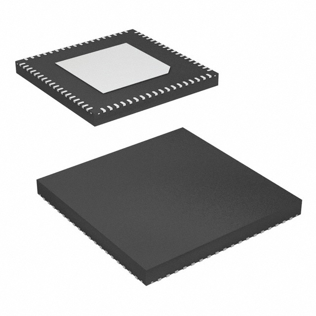


 工商网监
湘ICP备2023018690号
工商网监
湘ICP备2023018690号

