ADS5553
www.ti.com
SLWS158 − FEBRUARY 2005
Dual 14 BIT, 65 MSPS
Analog-to-Digital Converter
D
D
D
D
FEATURES
D Dual ADC
D 14 Bit Resolution
D 65 MSPS Sample Rate
D High SNR = 74 dBFs at 70 MHz fIN
D High SFDR = 84 dBc at 70 MHz fIN
D 2.3 VPP Differential Input Voltage
D Internal / External Voltage Reference
D 3.3 V Single-Supply Voltage
Analog Power Dissipation = 0.72 W
Output Supply Power Dissipation = 0.17 W
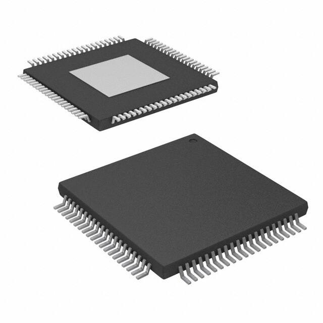
80 Lead PowerPadE TQFP Package
Two’s Complement Output Format
APPLICATIONS
D Communication Receivers
D Base Station Infrastructure
D Test and Measurement Instrumentation
DESCRIPTION
The ADS5553 is a high-performance, dual channel, 14 bit, 65 MSPS analog-to-digital converter (ADC). To provide
a complete solution, each channel includes a high-bandwidth linear sample-and-hold stage (S&H) and an internal
reference. Designed for applications demanding high dynamic performance in a small space, the ADS5553 has
excellent power consumption of 0.9 W at 3.3 V single-supply voltage. This allows an even higher system integration
density. The provided internal reference simplifies system design requirements, yet an external reference can be
used optionally to suit the accuracy and low drift requirements of the application. The outputs are parallel CMOS
compatible.
The ADS5553 is available in a 80 lead TQFP PowerPAD package and is specified over the full temperature range
of −40°C to 85°C.
DRVDD
AVDD
VREFP
VREFM
VIN+
VIN−
Internal Reference
S&H
14-Bit
Pipeline
ADC Core
CLK+
CLK+
VREFP
VREFM
D0
.
.
.
D13
Timing Circuitry
CLK−
VIN−
Output
Control
Timing Circuitry
CLK−
VIN+
Digital
Error
Correction
S&H
14-Bit
Pipeline
ADC Core
Internal Reference
AGND
Digital
Error
Correction
Output
Control
D0
.
.
.
D13
ADS5553
DRGND
Please be aware that an important notice concerning availability, standard warranty, and use in critical applications of Texas Instruments
semiconductor products and disclaimers thereto appears at the end of this data sheet.
CommsADC is a trademark of Texas Instruments.
PRODUCTION DATA information is current as of publication date. Products
conform to specifications per the terms of Texas Instruments standard warranty.
Production processing does not necessarily include testing of all parameters.
Copyright 2005, Texas Instruments Incorporated
�ADS5553
www.ti.com
SLWS158 − FEBRUARY 2005
PACKAGE/ORDERING INFORMATION(1)
PRODUCT
PACKAGE−LEAD
PACKAGE
DESIGNATOR
SPECIFIED
TEMPERATURE
RANGE
PACKAGE
MARKING
ADS5553
HTQFP 80((2))
HTQFP-80
PowerPAD
PFP
−40°C
40°C to 85°C
ADS5553I
(1)
(2)
TRANSPORT
MEDIA, QUANTITY
ADS5553IPFP
Tray, 96
ADS5553IPFPR
Tape and Reel, 1000
For the most current product and ordering information, see the Package Option Addendum located at the end of this data sheet.
Thermal pad size: 6.17 mm x 6.17 mm (min), 7,5 mm x 7,5 mm (max). θja = 21°C/W (no airflow) or 15°C/W (with 200 LPFM airflow),
θjc = 13.5°C/W, and θjp (to the bottom PowerPad) = 2°C/W when used with 2 oz. copper trace and pad soldered directly to a JEDEC standard
four layer 3 in x 3 in PCB.
ABSOLUTE MAXIMUM RATINGS
over operating free-air temperature range unless otherwise noted(1)
Supply
Voltage
AVDD to AGND,
DRVDD to DRGND
AGND to DRGND
ADS5553
UNIT
−0.3 to 3.7
V
This integrated circuit can be damaged by ESD. Texas
Instruments recommends that all integrated circuits be
handled with appropriate precautions. Failure to observe
proper handling and installation procedures can cause damage.
ESD damage can range from subtle performance degradation to
complete device failure. Precision integrated circuits may be more
susceptible to damage because very small parametric changes could
cause the device not to meet its published specifications.
±0.1
V
−0.3 to 3.6
V
Logic input to DRGND
−0.3 to DRVDD + 0.3
V
Digital data output to DRGND
−0.3 to DRVDD + 0.3
V
Operating temperature range
−40 to 85
°C
PARAMETER
105
°C
Supplies
−65 to 150
°C
Analog input to AGND(2)
Junction temperature
Storage temperature range
(1)
ORDERING
NUMBER
Stresses above these ratings may cause permanent damage.
Exposure to absolute maximum conditions for extended periods
may degrade device reliability. These are stress ratings only, and
functional operation of the device at these or any other conditions
beyond those specified is not implied.
(2) For more details, see the Input Voltage Overstress section in this
data sheet.
RECOMMENDED OPERATING CONDITIONS
MIN
TYP
MAX
UNIT
Analog supply voltage, AVDD
3
3.3
3.6
V
Output driver supply voltage,
DRVDD
3
3.3
3.6
V
Analog Input
Differential input range
Input common-mode voltage,
VCM(1)
2.3
1.45
1.55
VPP
1.65
V
Digital Output
Maximum output load
10
pF
Clock Input
ADCLK input sample rate (sine
wave) 1/tC
10
Clock amplitude, sine wave,
differential(2)
3
Clock duty cycle(3)
Open free-air temperature range
(1)
65
VPP
50%
−40
85
Input common-mode should be connected to CM.
(2) See Figure 20 for more information.
(3) See Figure 21 for more information.
2
MSPS
°C
�ADS5553
www.ti.com
SLWS158 − FEBRUARY 2005
ELECTRICAL CHARACTERISTICS
Typ, min, and max values at TA = 25°C, full temperature range is TMIN = −40°C to TMAX = 85°C, sampling rate = 65 MSPS, 50% clock duty
cycle, AVDD = DRVDD = 3.3 V, −1-dBFS differential input, 3-VPP differential clock, and internal reference, unless otherwise noted
PARAMETER
CONDITIONS
MIN
Resolution
TYP
MAX
UNIT
14
Bits
2.3
VPP
3.2
pF
Analog Inputs
Differential input range
Differential input capacitance
See Figure 28
200(1)
µA
750
MHz
Reference bottom voltage, VREFM
1.01
V
Reference top voltage, VREFP
2.16
V
Total gain error(2)
±3.5
%FS
Common-mode voltage output, VCM
1.57
V
Total analog input common-mode current
Analog input bandwidth
Source impedance = 50 Ω
Internal Reference Voltages
Dynamic Linearity and Accuracy
No missing codes
Tested
Differential linearity error, DNL
fIN = 46MHz
−0.95
±0.6
1
LSB
Integral linearity error, INL
fIN = 46 MHz
−4
±2.5
4
LSB
Offset error
±4
mV
Offset temperature coefficient
7
µV/°C
Offset matching
±0.7
mV
Gain error(3)
±0.5
%FS
0.0015
∆%/°C
±0.1
%FS
Gain temperature coefficient(3)
Gain matching(3)
Dynamic AC Characteristics
fIN = 10 MHz
74.4
fIN = 46 MHz
Signal-to-noise
Signal
to noise ratio, SNR
RMS output noise
fIN = 70 MHz
74
25°C to 85°C
72.4
Full temp range
71.4
74
fIN = 100 MHz
73.5
fIN = 150 MHz
72.5
fIN = 225 MHz
71
Input tied to common-mode
1
fIN = 10 MHz
85
fIN = 46 MHz
Spurious-free
Spurious
free dynamic range, SFDR
74
fIN = 70 MHz
dBFS
LSB
84
Room temp
80
84
Full temp range
78
83
fIN = 100 MHz
83
fIN = 150 MHz
81
fIN = 225 MHz
75
dBc
(1)
100-µA per input
Includes error due to references. The total gain error will become smaller (see gain error in the Dynamic Linearity and Accuracy section of this
table) if an external reference is used.
(3) Gain error left assuming ideal references: V
REFP − VREFM = 1.15 V
(2)
3
�ADS5553
www.ti.com
SLWS158 − FEBRUARY 2005
ELECTRICAL CHARACTERISTICS
Typ, min, and max values at TA = 25°C, full temperature range is TMIN = −40°C to TMAX = 85°C, sampling rate = 65 MSPS, 50% clock duty
cycle, AVDD = DRVDD = 3.3 V, −1-dBFS differential input, 3-VPP differential clock, and internal reference, unless otherwise noted
PARAMETER
CONDITIONS
MIN
fIN = 10 MHz
fIN = 70 MHz
80
86
Full temp range
78
85
fIN = 100 MHz
86
fIN = 150 MHz
82
fIN = 225 MHz
79
fIN = 10 MHz
85
Worst harmonic/spur
Worst-harmonic/spur
(other than HD2 and HD3)
Signal-to-noise
Signal
to noise + distortion, SINAD
fIN = 70 MHz
80
84
Full temp range
78
83
83
fIN = 150 MHz
81
fIN = 225 MHz
75
fIN = 10 MHz
Room temp
86
fIN = 70 MHz
Room temp
85
fIN = 10 MHz
74
fIN = 46 MHz
73.5
25°C to 85°C
Full temp range
Effective number of bits, ENOB
Two-tone intermodulation distortion, IMD3
Crosstalk
(4)
4
71.8
73.4
71
73
fIN = 100 MHz
73
fIN = 150 MHz
71.8
fIN = 225 MHz
69.5
fIN = 10 MHz
83
fIN = 46 MHz
Total harmonic distortion, THD
fIN = 70 MHz
dBc
dBc
dBFS
82
Room temp
82
Full temp range
82
fIN = 100 MHz
81
fIN = 150 MHz
81
fIN = 225 MHz
74
fIN = 70 MHz
11.9
f = 10.1 MHz, 15.1 MHz
(−7dBFS each tone)
94
f = 48 MHz, 53 MHz
(−7 dBFS each tone)
84
f = 147 MHz, 152 MHz
(−7 dBFS each tone)
75
fIN = 70 MHz(4)
dBc
84
Room temp
fIN = 100 MHz
fIN = 70 MHz
UNIT
93
Room temp
fIN = 46 MHz
Third-harmonic,
Third
harmonic, HD3
MAX
93
fIN = 46 MHz
Second-harmonic,
Second
harmonic, HD2
TYP
−100
dBc
Bits
dBc
−95
Inject one tone at −1 dBFS on one channel and measure the ampltitude on the other channel, then repeat for the other channel
dBc
�ADS5553
www.ti.com
SLWS158 − FEBRUARY 2005
ELECTRICAL CHARACTERISTICS
Typ, min, and max values at TA = 25°C, full temperature range is TMIN = −40°C to TMAX = 85°C, sampling rate = 65 MSPS, 50% clock duty
cycle, AVDD = DRVDD = 3.3 V, −1-dBFS differential input, 3-VPP differential clock, and internal reference, unless otherwise noted
PARAMETER
CONDITIONS
MIN
TYP
MAX
UNIT
Power Supply
Total supply current, ICC
VIN = full-scale, fIN = 70 MHz
270
288
mA
Analog supply current, IAVDD
VIN = full-scale, fIN = 70 MHz
220
230
mA
Output buffer supply current, IDRVDD
VIN = full-scale, fIN = 70 MHz, with
10 pF load on digital outputs to ground
50
58
mA
Analog only, fIN = 70 MHz
725
760
Digital power with 10-pF load on digital
outputs to ground, fIN = 70 MHz
165
190
Power dissipation with external reference
Total power with 10-pF load on digital
outputs to ground, fIN = 70 MHz
780
820
mW
Standby power
With clocks running (both channels
off and outputs disabled)
220
250
mW
Power dissipation
mW
DIGITAL CHARACTERISTICS
Typ, min, and max values at TA = 25°C, full temperature range is TMIN = −40°C to TMAX = 85°C, and AVDD = DRVDD = 3.3 V, unless otherwise
noted
CONDITIONS
PARAMETER
MIN
TYP
MAX
UNIT
Digital Inputs
High-level input voltage
2.4
V
Low-level input voltage
0.8
V
High-level input current
10
µA
Low-level input current
10
µA
Input capacitance
4
pF
Digital Outputs(1)
Low-level output voltage
CLOAD = 10 pF(2)
High-level output voltage
CLOAD = 10 pF(2)
0.3
2.8
Output capacitance
(1)
(2)
0.4
V
3
V
3
pF
For optimal performance, all digital output lines (D0:D13), including the output clock, should see a similar load.
Equivalent capacitance to ground of (load + parasitics of transmission lines).
5
�ADS5553
www.ti.com
SLWS158 − FEBRUARY 2005
TIMING CHARACTERISTICS
Analog
Input
Signal
Sample
N
N+1
N+2
N+3
N+4
N + 14
N + 16
N + 15
N + 17
tA
Input Clock
tSTART
tPDI = tSTART + tsu
Output Clock
tsu
Data Out
(D0−D11)
N − 17
N − 16
N − 15
tEND
N − 14
N − 13
N−3
N−2
N−1
N
Data Invalid
th
16.5 Clock Cycles
NOTE: It is recommended that the loading at CLKOUT and all data lines are accurately matched to ensure that the above timing
matches closely with the specified values.
Figure 1. Timing Diagram
TIMING CHARACTERISTICS(3)
Over full temperature range (TMIN = −40°C to TMAX = +85°C), sampling rate = 65 MSPS, 50% clock duty cycle, and AVDD = DRVDD = 3.3 V,
unless otherwise noted
PARAMETER
DESCRIPTION
MIN
TYP
MAX
UNIT
Switching Specification
Aperture delay, tA
Input CLK falling edge to data sampling point
1
ns
Aperture delay matching, tA
Channel-to-channel aperture delay matching
50
ps
Aperture jitter (uncertainty)
Uncertainty in sampling instant
300
fs
16.5
Clock
Cyles
4.3
6
ns
2
2.8
Latency
Data setup time, tsu
Data valid(1) to 50% of CLKOUT rising edge
Data hold time, th
50% of CLKOUT rising edge to data becoming invalid(1)
Data start time, tSTART
50% of clock input to beginning of valid data(1)
Data stop time, tEND
50% of clock input to end of valid data(1)
Data rise time, tr
Data rise time measured from 20% to 80% of DRVDD
Data fall time, tf
Data fall time measured from 80% to 20% of DRVDD
Data setup time, tsu
Data valid(1) to 50% of CLKOUT rising edge, fS = 40 MSPS
8.5
Data hold time, th
50% of CLKOUT rising edge to data becoming invalid(1),
fS = 40 MSPS
2.6
Data start time, tSTART
50% of clock input to beginning of valid data(1), FS = 40 MSPS
Data stop time, tEND
50% of clock input to end of valid data(1), FS = 40 MSPS
2.5
9
ns
10.6
ns
6.6
ns
5.5
ns
11
ns
4
ns
−2.5
1
ns
13
ns
Data rise time, tr
Data rise time measured from 20% to 80% of DRVDD,
fS = 40 MSPS
7.5
ns
Data fall time, tf
Data fall time measured from 80% to 20% of DRVDD,
fS = 40 MSPS
7.3
ns
Output enable (OE) to data output
delay
Time required for outputs to have stable timings with respect to
the input clock(2) after OE is activated
(1)
11.5
ns
4.5
1000
Clock
Cycles
Data valid refers to 2 V for logic high and 0.8 V for logic low.
Data outputs are available within a clock from assertion of OE; however it takes 1000 clock cycles to ensure stable timing with respect to input
clock.
(3): Timing parameters are ensured by design and characterization and not tested in production.
(2):
6
�ADS5553
www.ti.com
SLWS158 − FEBRUARY 2005
PIN CONFIGURATION
AVDD
AGND
INPA
INMA
AGND
AVDD
AGND
AVDD
OVRA
D13A (MSB)
D12A
D11A
D10A
D9A
DRGND
DRVDD
D8A
D7A
D6A
D5A
PFP PACKAGE
(TOP VIEW)
80 79 78 77 76 75 74 73 72 71 70 69 68 67 66 65 64 63 62 61
1
60
2
59
3
58
4
57
5
56
6
55
7
54
8
9
10
11
12
ADS5553
PowerPad
(Connect
to AGND)
53
52
51
50
49
13
48
14
47
15
46
16
45
17
44
18
43
19
42
20
41
21 22 23 24 25 26 27 28 29 30 31 32 33 34 35 36 37 38 39 40
D4A
D3A
DRGND
DRVDD
D2A
D1A
D0A (LSB)
CLKOUTA
OEA
REFSEL
PDN
DRVDD
OEB
CLKOUTB
OVRB
D13B (MSB)
D12B
D11B
DRVDD
DRGND
AVDD
AGND
INMB
INPB
AGND
AVDD
AVDD
D0B (LSB)
D1B
D2B
D3B
D4B
DRGND
DRVDD
D5B
D6B
D7B
D8B
D9B
D10B
CMA
AGND
CLKPA
CLKMA
AGND
REFMA
REFPA
AVDD
AVDD
IREF
AVDD
AGND
AVDD
REFMB
REFPB
AGND
CLKPB
CLKMB
AGND
CMB
7
�ADS5553
www.ti.com
SLWS158 − FEBRUARY 2005
PIN ASSIGNMENTS
TERMINAL
NO.
NAME
NO.
OF PINS
I/O
AVDD
8, 9, 11,
13, 21, 26,
27, 73, 75,
80
10
I
Analog power supply
AGND
2, 5, 12,
16, 19, 22,
25, 74, 76,
79
10
I
Analog ground
CLKMA
4
1
I
Channel A differential input clock (negative)
CLKMB
18
1
I
Channel B differential input clock (negative)
CLKOUTA
53
1
O
Channel A clock out in sync with data
1
O
Channel B clock out in sync with data
CLKOUTB
DESCRIPTION
CLKPA
3
1
I
Channel A differential input clock (positive)
CLKPB
17
1
I
Channel B differential input clock (positive)
CMA
1
1
O
Channel A common-mode output voltage
CMB
20
1
O
Channel B common-mode output voltage
D0A (LSB)−D13A (MSB)
54−56,
59−64,
67−71
14
O
Channel A parallel data
D0B (LSB)−D13B (MSB)
28−32,
35−40,
43−45
14
O
Channel B parallel data
DRVDD
34, 42,
49, 57, 65
4
I
Output driver power supply
DRGND
33, 41,
58, 66
4
I
Output driver ground
INMA
77
1
I
Channel A differential analog input (negative)
INMB
23
1
I
Channel B differential analog input (negative)
INPA
78
1
I
Channel A differential analog input (positive)
INPB
24
1
I
Channel B differential analog input (positive)
IREF
10
1
I
Current set, 56-kΩ resistor to GND
OEA
52
1
I
Channel A output enable (active high)
OEB
48
1
I
Channel B output enable (active high)
OVRA
72
1
O
Channel A over-range indicator bit
OVRB
46
1
O
Channel B over-range indicator bit
REFMA
6
1
I
Channel A reference voltage (negative); 0.1 µF to GND
REFMB
14
1
I
Channel B reference voltage (negative); 0.1 µF to GND
REFPA
7
1
I
Channel A reference voltage (positive); 0.1 µF to GND
REFPB
15
1
I
Channel B reference voltage (positive); 0.1 µF to GND
PDN
50
1
I
Power down active high. See Table 2
REFSEL
51
1
I
Reference select. 1 → EXT. REF; 0 → INT. REF
8
�ADS5553
www.ti.com
SLWS158 − FEBRUARY 2005
DEFINITION OF SPECIFICATIONS
Analog Bandwidth
The analog input frequency at which the power of the
fundamental is reduced by 3 dB with respect to the low
frequency value.
Aperture Delay
The delay between the falling edge of the input
sampling clock and the actual time at which the
sampling occurs.
Aperture Uncertainty (Jitter)
The sample-to-sample variation in aperture delay.
Clock Pulse Width/Duty Cycle
The duty cycle of a clock signal is the ratio of the time
the clock signal remains at a logic high (clock pulse
width) to the period of the clock signal. Duty cycle is
typically expressed as a percentage. A perfect
differential sine wave clock results in a 50% duty cycle.
Maximum Conversion Rate
The maximum sampling rate at which certified
operation is given. All parametric testing is performed
at this sampling rate unless otherwise noted.
Minimum Conversion Rate
The minimum sampling rate at which the ADC
functions.
Differential Nonlinearity (DNL)
An ideal ADC exhibits code transitions at analog input
values spaced exactly 1LSB apart. The DNL is the
deviation of any single step from this ideal value,
measured in units of LSBs.
Integral Nonlinearity (INL)
The INL is the deviation of the ADC’s transfer function
from a best fit line determined by a least squares curve
fit of that transfer function, measured in units of LSBs.
Gain Error
The gain error is the deviation of the ADC’s actual input
full-scale range from its ideal value. The gain error is
given as a percentage of the ideal input full-scale range.
Gain error does not account for variations in the internal
reference voltages (see the Electrical Specifications
section for limits on the variation of VREFP and VREFM).
Offset Error
The offset error is the difference, given in number of
LSBs, between the ADC’s actual average idle channel
output code and the ideal average idle channel output
code. This quantity is often mapped into mV.
Temperature Drift
The temperature drift coefficient (with respect to gain
error and offset error) specifies the change per degree
celcius of the parameter from TMIN to TMAX. It is
calcuated by dividing the maximum deviation of the
parameter across the TMIN to TMAX range by the
difference TMAX−TMIN.
Signal-to-Noise Ratio
SNR is the ratio of the power of the fundamental (PS)
to the noise floor power (PN), excluding the power at DC
and the first eight harmonics.
SNR + 10Log 10
PS
PN
SNR is either given in units of dBc (dB to carrier) when
the absolute power of the fundamental is used as the
reference, or dBFS (dB to full scale) when the power of
the fundamental is extrapolated to the converter’s
full-scale range.
Signal-to-Noise and Distortion (SINAD)
SINAD is the ratio of the power of the fundamental (PS)
to the power of all the other spectral components
including noise (PN) and distortion (PD), but excluding
DC.
SINAD + 10Log 10
PS
PN ) PD
SINAD is either given in units of dBc (dB to carrier) when
the absolute power of the fundamental is used as the
reference, or dBFS (dB to full scale) when the power of
the fundamental is extrapolated to the converter’s
full-scale range.
Effective Number of Bits (ENOB)
The ENOB is a measure of a converter’s performance
as compared to the theoretical limit based on
quantization noise.
ENOB + SINAD * 1.76
6.02
9
�ADS5553
www.ti.com
SLWS158 − FEBRUARY 2005
DEFINITION OF SPECIFICATIONS
Total Harmonic Distortion (THD)
THD is the ratio of the power of the fundamental (PS) to
the power of the first eight harmonics (PD).
THD + 10Log 10
PS
PD
THD is typically given in units of dBc (dB to carrier).
Spurious-Free Dynamic Range (SFDR)
The ratio of the power of the fundamental to the highest
other spectral component (either spur or harmonic).
SFDR is typically given in units of dBc (dB to carrier).
10
Two-Tone Intermodulation Distortion
IMD3 is the ratio of the power of the fundamental (at
frequencies f1 and f2) to the power of the worst spectral
component at either frequency 2f1−f2 or 2f2−f1. IMD3 is
either given in units of dBc (dB to carrier) when the
absolute power of the fundamental is used as the
reference, or dBFS (dB to full scale) when the power of
the fundamental is extrapolated to the converter’s
full-scale range.
�ADS5553
www.ti.com
SLWS158 − FEBRUARY 2005
TYPICAL CHARACTERISTICS
Typical values are at TA = 25°C, AVDD = DRVDD = 3.3 V, differential input amplitude = −1 dBFS, sampling rate = 65 MSPS, unless otherwise
noted
SPECTRAL PERFORMANCE
SPECTRAL PERFORMANCE
0
0
Amplitude − dBFS
−40
−60
−80
−100
−40
−60
−80
−100
−120
−140
fS = 65 MSPS
fIN = 10 MHz
SNR = 74.6 dBFS
SINAD = 74.3 dBFS
SFDR = 84.7 dBc
THD = 84.3 dBc
−20
Amplitude − dBFS
fS = 65 MSPS
fIN = 2.2 MHz
SNR = 74.2 dBFS
SINAD = 73.9 dBFS
SFDR = 86.1 dBc
THD = 83.6 dBc
−20
0
5
10
15
20
25
−120
30
0
5
Figure 3
30
SPECTRAL PERFORMANCE
fS = 65 MSPS
fIN = 46 MHz
SNR = 74.1 dBFS
SINAD = 73.8 dBFS
SFDR = 85.2 dBc
THD = 83.5 dBc
−40
−60
fS = 65 MSPS
fIN = 70.2 MHz
SNR = 74.2 dBFS
SINAD = 73.8 dBFS
SFDR = 84.3 dBc
THD = 83.6 dBc
−20
Amplitude − dBFS
Amplitude − dBFS
25
0
−20
−80
−100
−120
−40
−60
−80
−100
−120
0
5
10
15
20
25
−140
30
0
5
10
15
20
f − Frequency − MHz
f − Frequency − MHz
Figure 4
Figure 5
SPECTRAL PERFORMANCE
25
30
SPECTRAL PERFORMANCE
0
0
fS = 65 MSPS
fIN = 100.2 MHz
SNR = 73.8 dBFS
SINAD = 73 dBFS
SFDR = 79.9 dBc
THD = 79.7 dBc
−40
−60
fS = 65 MSPS
fIN = 150.1 MHz
SNR = 72.9 dBFS
SINAD = 72.1 dBFS
SFDR = 81.7 dBc
THD = 79.3 dBc
−20
Amplitude − dBFS
−20
Amplitude − dBFS
20
Figure 2
SPECTRAL PERFORMANCE
−80
−100
−120
−140
15
f − Frequency − MHz
0
−140
10
f − Frequency − MHz
−40
−60
−80
−100
−120
0
5
10
15
20
25
30
−140
0
5
10
15
20
f − Frequency − MHz
f − Frequency − MHz
Figure 6
Figure 7
25
30
11
�ADS5553
www.ti.com
SLWS158 − FEBRUARY 2005
TYPICAL CHARACTERISTICS
Typical values are at TA = 25°C, AVDD = DRVDD = 3.3 V, differential input amplitude = −1 dBFS, sampling rate = 65 MSPS, unless otherwise
noted
SPECTRAL PERFORMANCE
SPECTRAL PERFORMANCE
0
0
fS = 65 MSPS
fIN = 225 MHz
SNR = 71.8 dBFS
SINAD = 70.2 dBFS
SFDR = 76.9 dBc
THD = 74 dBc
−40
−60
−80
−100
−120
−140
fS = 65 MSPS
fIN = 300 MHz
SNR = 69.7 dBFS
SINAD = 67.8 dBFS
SFDR = 71.9 dBc
THD = 71.4 dBc
−20
Amplitude − dBFS
Amplitude − dBFS
−20
−40
−60
−80
−100
−120
0
5
10
15
20
25
−140
30
0
5
fS = 65 MSPS
fIN 1 = 10 MHz, −7 dBFS
fIN 2 = 15 MHz, −7 dBFS
IMD3 = −100 dBFS
SFDR = 83 dBc
Amplitude − dBFS
2
F
1
+
2
F
2
2
F
F1
1−
−F
F2
2
2
F
2F
+1
F+
1F
2
2
F
32
F+
2F
1
2
F
1
+
F3
2 F
1
−40
−60
−80
0
5
10
15
20
3
F
1
2
F
1
+
F
2
2
F
1
−
F
2
25
−140
30
−60
2
F
2
+
F
1
−80
−100
F
1
−
3 F
F 2
2
5
10
15
20
f − Frequency − MHz
Figure 10
Figure 11
F
1
2
F
2
+
F
1
F
1
+
F
2
3
F
2
30
40
35
30
F
1
−
F
2
2
F
1
+
F
2
25
NOISE HISTOGRAM WITH INPUTS SHORTED
F
2
F
1
+
F
2
2
F
1
+
F
2
3
F
1
Percentage − %
−40
0
f − Frequency − MHz
fS = 65 MSPS
fIN 1 = 148 MHz, −7 dBFS
fIN 2 = 153 MHz, −7 dBFS
IMD3 = −81 dBFS
SFDR = 73 dBc
2
−20
Amplitude − dBFS
2
F
2
−
F
1
−100
SPECTRAL PERFORMANCE
2
F
2
−
F
1
25
20
15
10
−120
12
F
1
−
F
2
fS = 65 MSPS
fIN 1 = 48 MHz, −7 dBFS
fIN 2 = 53 MHz, −7 dBFS
IMD3 = −91 dBFS
SFDR = 84 dBc
−120
0
−140
F
1
F
2
−20
−120
−140
30
SPECTRAL PERFORMANCE
0
Amplitude − dBFS
F
2
−40
−100
25
Figure 9
−20
−80
20
Figure 8
F
1
−60
15
f − Frequency − MHz
SPECTRAL PERFORMANCE
0
10
f − Frequency − MHz
5
0
5
10
15
20
25
30
0
8213 8214 8215 8216 8217 8218 8219 8220 8221 8222
f − Frequency − MHz
Code Number
Figure 12
Figure 13
�ADS5553
www.ti.com
SLWS158 − FEBRUARY 2005
TYPICAL CHARACTERISTICS
Typical values are at TA = 25°C, AVDD = DRVDD = 3.3 V, differential input amplitude = −1 dBFS, sampling rate = 65 MSPS, unless otherwise
noted
WCDMA CARRIER
WCDMA CARRIER
0
0
fS = 61.4 MSPS
fIN = 70 MHz
PAR = 5 dB
ACPR Adj Top = 76.9 dB
ACPR Adj Low = 75.9 dB
−40
−60
−80
−100
−120
−140
0
5
10
15
20
25
−60
−80
−100
−140
30
25
AC PERFORMANCE
vs
INPUT AMPLITUDE
30
120
100
SFDR (dBFS)
SNR (dBFS)
SFDR (dBc)
0
−70
−60
−50
−40
−30
−20
−10
SNR (dBFS)
60
SFDR (dBc)
40
20
SNR (dBc)
0
fS = 65 MSPS
fIN = 46 MHz
−80
SFDR (dBFS)
80
−20
−90
0
fS = 65 MSPS
fIN = 150 MHz
−80
−70
−60
−50
−40
−30
−20
AIN − Input Amplitude − dBFS
AIN − Input Amplitude − dBFS
Figure 16
Figure 17
AC PERFORMANCE
vs
INPUT AMPLITUDE
POWER DISSIPATION
vs
SAMPLING RATE
120
1.00
100
0.95
40
20
AC PERFORMANCE
vs
INPUT AMPLITUDE
SNR (dBc)
60
15
Figure 15
20
−20
−90
10
Figure 14
AC Performance − dB
40
5
f − Frequency − MHz
80
60
0
f − Frequency − MHz
PD − Power Dissipation − W
AC Performance − dB
100
AC Performance − dB
−40
−120
120
80
fS = 61.4 MSPS
fIN = 170 MHz
PAR = 5 dB
ACPR Adj Top = 73.3 dB
ACPR Adj Low = 74.1 dB
−20
Amplitude − dBFS
Amplitude − dBFS
−20
SFDR (dBFS)
SNR (dBFS)
SFDR (dBc)
20
SNR (dBc)
0
fS = 65 MSPS
fIN = 225 MHz
−20
−100 −90 −80 −70 −60 −50 −40 −30 −20 −10
AIN − Input Amplitude − dBFS
Figure 18
0
−10
0
fIN = 46 MHz
0.90
0.85
0.80
0.75
0.70
10
20
30
40
50
60
70
80
fS − Sampling Rate − MSPS
Figure 19
13
�ADS5553
www.ti.com
SLWS158 − FEBRUARY 2005
TYPICAL CHARACTERISTICS
Typical values are at TA = 25°C, AVDD = DRVDD = 3.3 V, differential input amplitude = −1 dBFS, sampling rate = 65 MSPS, unless otherwise
noted
AC PERFORMANCE
vs
DIFFERENTIAL CLOCK AMPLITUDE
AC PERFORMANCE
vs
DUTY CYCLE
90
90
85
87
SFDR SE (dBc)
80
SNR SE (dBFS)
75
70
SNR Diff (dBFS)
86
85
84
83
82
65
81
fIN = 46 MHz
60
fIN = 20 MHz
88
SFDR − dBc
AC Performance − dB
89
SFDR Diff (dBc)
0
1
2
3
4
80
5
30
35
88
AC Performance − dB
AC Performance − dB
90
fIN = 46 MHz
SFDR (dBc)
84
82
80
78
76
65
70
SNR (dBFS)
74
fIN = 46 MHz
SFDR (dBc)
86
84
82
80
78
76
SNR (dBFS)
74
72
3.1
3.2
3.3
3.4
3.5
70
3.0
3.6
3.1
AVDD − Analog Supply Voltage − V
3.2
86
3.5
3.6
AC PERFORMANCE
vs
DIGITAL SUPPLY VOLTAGE
86
fIN = 150 MHz
fIN = 150 MHz
84
AC Performance − dB
84
SFDR (dBc)
80
78
76
SNR (dBFS)
74
3.4
Figure 23
AC PERFORMANCE
vs
ANALOG SUPPLY VOLTAGE
82
3.3
DRVDD − Digital Supply Voltage − V
Figure 22
AC Performance − dB
60
AC PERFORMANCE
vs
DIGITAL SUPPLY VOLTAGE
72
72
82
SFDR (dBc)
80
78
76
74
SNR (dBFS)
72
3.1
3.2
3.3
3.4
AVDD − Analog Supply Voltage − V
Figure 24
14
55
Figure 21
86
70
3.0
50
Figure 20
90
70
3.0
45
Duty Cycle − %
AC PERFORMANCE
vs
ANALOG SUPPLY VOLTAGE
88
40
Differential Clock Amplitude − V
3.5
3.6
70
3.0
3.1
3.2
3.3
3.4
DRVDD − Digital Supply Voltage − V
Figure 25
3.5
3.6
�ADS5553
www.ti.com
SLWS158 − FEBRUARY 2005
Typical values are at TA = 25°C, AVDD = DRVDD = 3.3 V, differential input amplitude = −1 dBFS, sampling rate = 65 MSPS, unless otherwise
noted
80
74
70
fS − Sampling Frequency − MHz
71
73
69
70
60
72
68
69
71
50
74
73
70
40
71
30
75
72
10
70
71
64
66
100
50
65
67
66
68
67
74
67
66
68
70
69
73
20
68
69
72
64
65
63
61
62
200
150
63
62
60
300
250
fIN − Input Frequency − MHz
60
65
70
75
SNR − dBFS
Figure 26.
80
85
83
83
85
81
fS − Sampling Frequency − MHz
70
81
85
83
40
85
87
83
85
87
85
85
79
20
85
73
75
83
87 87
81 79
77
75
71
50
79
77
75
77
73
71
83
85
30
10
83 81
81
89
77
79
83
87
85
81
71
87
87
83
85
85
60 87
50
85
83 83
77
75
73
73
71
69
71
69
69
67
67
65
65
100
150
61
63
250
200
67
65
63
59
300
fIN − Input Frequency − MHz
55
60
65
70
75
80
85
SFDR − dBc
Figure 27.
15
�ADS5553
www.ti.com
SLWS158 − FEBRUARY 2005
APPLICATION INFORMATION
THEORY OF OPERATION
The ADS5553 is a low-power, dual 14 bit, 65 MSPS,
CMOS, switched capacitor, pipeline ADC that operates
from a single 3.3 V supply. The conversion process is
initiated by a falling edge of the external input clock.
Once the signal is captured by the input S&H, the input
sample is sequentially converted by a series of small
resolution stages, with the outputs combined in a digital
correction logic block. Both the rising and the falling
clock edges are used to propagate the sample through
the pipeline every half clock cycle. This process results
in a data latency of 16.5 clock cycles, after which the
output data is available as a 14 bit parallel word, coded
in binary two’s complement format.
INPUT CONFIGURATION
The analog input for the ADS5553 consists of a
differential sample-and-hold architecture implemented
using a switched capacitor technique, shown in
Figure 28.
S3a
L1
C1a
R1a
INP
S1a
CP1
CP3
L2
+
C1b
R1b
INM
R3
S3
CA
−
CP2
CP4
S3b
L1, L2, : 6 nH to 10 nH effective
R1a, R1b : 5 Ω to 8 Ω
C1a, C1b : 2.2 pF to 2.6 pF
CP1, CP2 : 1.8 pF to 2.2 pF
CP3, CP4 : 1.2 pF to 1.8 pF
CA : 0.8 pF to 1.2 pF
R3 : 80 Ω to 120 Ω
Switches : S1a, S1b : On Resistance : 35 Ω to 50 Ω
S2, : On Resistance : 7.5 Ω to 15 Ω
S3a, S3b : On Resistance : 40 Ω to 60 Ω
All switches Off Resistance : 10 GΩ
All switches are on in sampling phase which is approximately one half of a clock period.
Figure 28. Analog Input Stage
16
VINCM
1V
�ADS5553
www.ti.com
SLWS158 − FEBRUARY 2005
This differential input topology produces a high level of
ac performance for high sampling rates. It also results
in a high usable input bandwidth, especially important
for high intermediate-frequency (IF) or undersampling
applications. The ADS5553 requires each of the analog
inputs (INP, INM) to be externally biased around the
common-mode level of the internal circuitry (CM, pins
1 and 20). For a full-scale differential input, each of the
differential lines of the input signal swings symmetrically
between CM + 0.575 V and CM – 0.575 V. This means
that each input is driven with a signal of up to CM ±0.575
V, so that each input has a maximum differential signal
of 1.15 VPP for a total differential input signal swing of
2.3 VPP. The maximum swing is determined by the two
reference voltages, the top reference (REFPA, pin 7
and REFPB, pin 15) and the bottom reference (REFMA,
pin 6 and REFMB, pin 18).
The ADS5553 obtains optimum performance when the
analog inputs are driven differentially. The circuit shown
in Figure 29 shows one possible configuration using an
RF transformer.
R0
50 Ω
Z0
50 Ω
25 Ω
1:1
25 Ω
AC
Signal
Source
100 nF
INP
ADS5553
25 Ω
ADT1−1WT
INM
25 Ω
CM
10 Ω
100 nF
0.1 µF
Figure 29. Transformer Input to Convert
Single-Ended Signal to Differential Signal
The single-ended signal is fed to the primary winding of
an RF transformer. Since the input signal must be
biased around the common-mode voltage of the
internal circuitry, the common-mode voltage (VCM) from
the ADS5553 is connected to the center-tap of the
secondary winding. To ensure a steady low-noise VCM
reference, best performance is obtained when the CM
output (pins 1 and 20) is filtered to ground with a 10 Ω
series resistor and parallel 0.1 µF and 0.001 µF
low-inductance capacitors as shown in Figure 29.
Output VCM (pins 1 and 20) is designed to directly drive
the ADC input. When providing a custom CM level, be
aware that the input structure of the ADC sinks a
common-mode current in the order of 200 µA (100 µA
per input). Equation (1) describes the dependency of
the common-mode current and the sampling
frequency:
20)
400 mA f s(in MSPS)
125MSPS
(1)
This equation helps to design the output capability and
impedance of the driving circuit accordingly.
When it is necessary to buffer or apply a gain to the
incoming analog signal, it is possible to combine
single-ended operational amplifiers with an RF
transformer, or to use a differential input/output
amplifier without a transformer, to drive the input of the
ADS5553. Texas Instruments offers a wide selection of
single-ended operational amplifiers (including the
THS3201, THS3202, OPA847, and OPA695) that can
be selected depending on the application. An RF gain
block amplifier, such as Texas Instruments THS9001,
can also be used with an RF transformer for high input
frequency applications. The THS4503/6 are
recommended differential input/output amplifiers.
Table 1 lists the recommended amplifiers.
When using single-ended operational amplifiers (such
as the THS3201, THS3202, OPA847, or OPA695) to
provide gain, a three-amplifier circuit is recommended
with one amplifier driving the primary of an RF
transformer and one amplifier in each of the legs of the
secondary driving the two differential inputs of the
ADS5553. These three amplifier circuits minimize
even-order harmonics. For high frequency inputs, an
RF gain block amplifier can be used to drive a
transformer primary; in this case, the transformer
secondary connections can drive the input of the
ADS5553 directly, as shown in Figure 29 or with the
addition of the filter circuit shown in Figure 30.
Figure 30 illustrates how RIN and CIN can be placed to
isolate the signal source from the switching inputs of the
ADC and to implement a low-pass RC filter to limit the
input noise in the ADC. It is recommended that these
components be included in the ADS5553 circuit layout
when any of the amplifier circuits discussed previously
are used. The components allow fine-tuning of the
circuit performance. Any mismatch between the
differential lines of the ADS5553 input produces a
degradation in performance at high input frequencies,
mainly characterized by an increase in the even-order
harmonics. In this case, special care should be taken to
keep as much electrical symmetry as possible between
both inputs.
Another possible configuration for lower-frequency
signals is the use of differential input/output amplifiers
that can simplify the driver circuit for applications
17
�ADS5553
www.ti.com
SLWS158 − FEBRUARY 2005
requiring dc coupling of the input. Flexible in their
configurations (see Figure 31), such amplifiers can be
used for single-ended-to-differential conversion, signal
amplification.
Table 1. Recommended Amplifiers to Drive the Input of the ADS5553
INPUT SIGNAL FREQUENCY
RECOMMENDED AMPLIFIER
TYPE OF AMPLIFIER
USE WITH TRANSFORMER?
DC to 20 MHz
THS4503/6
Differential In/Out Amp
No
DC to 50 MHz
OPA847
Operational Amp
Yes
OPA695
Operational Amp
Yes
10 MHz to 120 MHz
THS3201
Operational Amp
Yes
THS3202
Operational Amp
Yes
THS9001
RF Gain Block
Yes
Over 100 MHz
5V
VIN
−5 V
RS
100 Ω
+
OPA695
−
0.1 µF
RT
100 Ω
1000 pF
R1
400 Ω
RIN
1:1
RIN
AINP
ADS5553
CIN
AINM
10 Ω
AV = 8V/V
(18 dB)
R2
57.5 Ω
CM
0.1 mF
Figure 30. Converting a Single-Ended Input Signal to a Differential Signal Using an RF Transformer
RS
RG
RT
RF
5V
3.3 V
10 µF
0.1 µF
RIN
VOCM
1 µF
RIN
THS4503
10 µF
RG
−5 V
INP
INM
ADS5553
14-Bit/65 MSPS
0.1 µF
RF
Figure 31. Using the THS4503 With the ADS5553
18
CM
10 Ω
0.1 µF
�ADS5553
www.ti.com
SLWS158 − FEBRUARY 2005
INPUT VOLTAGE OVER-STRESS
The ADS5553 can handle absolute maximum voltages
of 3.6 V DC on the input pins INP and INM. For DC
inputs between 3.6 V and 3.8 V, a 25 Ω resistor is
required in series with the input pins. For inputs above
3.8 V, the device can handle only transients, which need
to have less than 5% duty cycle of overstress. The input
pins connect internally to an ESD diode to AVDD, as well
as a switched capacitor circuit. The sampling capacitor
of the switched capacitor circuit connects to the input
pins through a switch in the sample phase. In this
phase, an input larger then 2.65 V would cause the
switched capacitor circuit to present an equivalent load
of a forward biased diode to 2.65 V, in series with a 60Ω
impedance. Also, beyond the voltage on AVDD, the ESD
diode to AVDD starts to become forward biased.
In the phase where the sampling switch is off, the diode
loading from the input switched capacitor circuit is
disconnected from the pin, while the ESD loading to
AVDD is still present.
CAUTION:
A violation of any of the previously stated
conditions could damage the device (or reduce
its lifetime) either due to electromigration or
gate oxide integrity. Care should be taken not
to expose the device to input over-voltage for
extended periods of time as it may degrade
device reliability.
POWER SUPPLY SEQUENCE
The preferred mode of power supply sequencing is to
power up AVDD first, followed by DRVDD. Raising both
supplies simultaneously is also a valid power supply
sequence. In the event that DRVDD powers up before
AVDD in the system, AVDD must power up within 10 ms
of DRVDD.
POWER DOWN
The device enters power down in one of two ways:
either by reducing the clock speed to between dc and
1 MHz or by selecting any of the modes in Table 2. If
reducing the clock speed, power-down may be initiated
for any clock frequency below 10 MHz. The actual
frequency at which the device powers down varies from
device to device.
Table 2. Powerdown Mode Selection
PDN
(Pin 50)
OEA
(Pin 52)
OEB
(Pin 48)
Out A
Out B
ADC A
ADC B
0
0
0
Off
Off
On
On
0
0
1
Off
On
On
On
0
1
0
On
Off
On
On
0
1
1
On
On
On
On
1
0
0
Off
Off
Off
Off
1
0
1
Off
On
Off
On
1
1
0
On
Off
On
Off
1
1
1
On
On
On
On
REFERENCE CIRCUIT
The ADS5553 has built-in internal reference
generation, requiring no external circuitry on the printed
circuit board (PCB). For optimum performance, it is best
to connect both REFP and REFM to ground with a 1 µF
decoupling capacitor in series with a 20 Ω resistor, as
shown in Figure 32. In addition, an external 56.2-kΩ
resistor should be connected from IREF (pin 10) to
AGND to set the proper current for the operation of the
ADC, as shown in Figure 32. No capacitor should be
connected between pin 31 and ground; only the 56.2 kΩ
resistor should be used.
20 Ω
29 REFP
1 µF
20 Ω
30 REFM
1 µF
31 IREF
56 kΩ
Figure 32. REFP, REFM, and IREF Connections
for Optimum Performance
19
�ADS5553
www.ti.com
SLWS158 − FEBRUARY 2005
CLOCK INPUT
The ADS5553 clock input can be driven with either a
differential clock signal or a single-ended clock input,
with little or no difference in performance between both
configurations. The common-mode voltage of the clock
inputs is set internally to CM using internal 5-kΩ
resistors that connect CLKP and CLKM to CM , as
shown in Figure 33.
CM
CM
5 kΩ
5 kΩ
CLKP
CLKM
6 pF
3 pF
3 pF
Figure 33. Clock Inputs
When driven with a single-ended CMOS clock input, it
is best to connect CLKM to ground with a 0.01 µF
capacitor, while CLKP is ac-coupled with a 0.01 µF
capacitor to the clock source, as shown in Figure 34.
Square Wave or
Sine Wave
CLKP
0.01 µF
ADS5553
CLKM
0.01 µF
Figure 34. AC-Coupled, Single-Ended Clock Input
The ADS5553 clock input can also be driven
differentially, reducing susceptibility to common-mode
noise. In this case, it is best to connect both clock inputs
to the differential input clock signal with 0.01 µF
capacitors, as shown in Figure 35.
20
CLKP
Differential Square Wave
or Sine Wave
(3 Vp-p)
0.01 µF
ADS5553
CLKM
0.01 µF
Figure 35. AC-Coupled, Differential Clock Input
For high input frequency sampling, it is recommended
to use a clock source with low jitter. Additionally, the
internal ADC core uses both edges of the clock for the
conversion process. This means that, ideally, a 50%
duty cycle should be provided. Figure 24 shows the
performance variation of the ADC versus clock duty
cycle.
Bandpass filtering of the source can help produce a
50% duty cycle clock and reduce the effect of jitter.
When using a sinusoidal clock, the clock jitter further
improves as the amplitude is increased. In that sense,
using a differential clock allows for the use of larger
amplitudes without exceeding the supply rails and
absolute maximum ratings of the ADC clock input.
Figure 23 shows the performance variation of the
device versus input clock amplitude. For detailed
clocking schemes based on transformer or PECL-level
clocks, see the ADS5553EVM user’s guide
(SLWU010), available for download from www.ti.com.
�ADS5553
www.ti.com
SLWS158 − FEBRUARY 2005
OUTPUT INFORMATION
Assembly Process
Each of the two ADCs provide 14 data outputs in two’s
complement format (D13 to D0, with D13 being the
MSB and D0 the LSB), a data-ready signal (CLKOUT),
and an out-of-range indicator (OVR) that equals 1 when
the output reaches the full-scale limits.
1. Prepare the PCB top-side etch pattern including
etch for the leads as well as the thermal pad as
illustrated in the Mechanical Data section.
In addition, output enable control (pins 48 and 52) are
provided to tri-state the outputs. See Table 2 for details.
The output circuitry of the ADS5553 has been designed
to minimize the noise produced by the transients of the
data switching and in particular its coupling to the ADC
analog circuitry. Output D0 senses the load capacitance
and adjusts the drive capability of all the output pins of
the ADC to maintain the same output slew rate
described in the timing diagram of Figure 1, as long as
all outputs (including CLKOUT) have a similar load as
the one at D0. This circuit also reduces the sensitivity
of the output timing versus supply voltage or
temperature. External series resistors with the output
are not necessary.
PowerPAD PACKAGE
The PowerPAD package is a thermally enhanced
standard size IC package designed to eliminate the use
of bulky heatsinks and slugs traditionally used in
thermal packages. This package can be easily mounted
using standard printed circuit board (PCB) assembly
techniques, and can be removed and replaced using
standard repair procedures.
The PowerPAD package is designed so that the
leadframe die pad (or thermal pad) is exposed on the
bottom of the IC. This provides an extremely low
thermal resistance path between the die and the
exterior of the package. The thermal pad on the bottom
of the IC can then be soldered directly to the printed
circuit board (PCB), using the PCB as a heatsink.
2. Place a 5-by-5 array of thermal vias in the thermal
pad area. These holes should be 13 mils in
diameter. The small size prevents wicking of the
solder through the holes.
3. It is recommended to place a small number of 25 mil
diameter holes under the package, but outside the
thermal pad area to provide an additional heat path.
4. Connect all holes (both those inside and outside the
thermal pad area) to an internal copper plane (such
as a ground plane).
5. Do not use the typical web or spoke via connection
pattern when connecting the thermal vias to the
ground plane. The spoke pattern increases the
thermal resistance to the ground plane.
6. The top-side solder mask should leave exposed the
terminals of the package and the thermal pad area.
7. Cover the entire bottom side of the PowerPAD vias
to prevent solder wicking.
8. Apply solder paste to the exposed thermal pad area
and all of the package terminals.
For more detailed information regarding the PowerPAD
package and its thermal properties, see either the
SLMA004B Application Brief PowerPAD Made Easy or
the SLMA002 Technical Brief PowerPAD Thermally
Enhanced Package.
21
�PACKAGE OPTION ADDENDUM
www.ti.com
10-Dec-2020
PACKAGING INFORMATION
Orderable Device
Status
(1)
Package Type Package Pins Package
Drawing
Qty
Eco Plan
(2)
Lead finish/
Ball material
MSL Peak Temp
Op Temp (°C)
Device Marking
(3)
(4/5)
(6)
ADS5553IPFP
ACTIVE
HTQFP
PFP
80
96
RoHS & Green
NIPDAU
Level-3-260C-168 HR
-40 to 85
ADS5553I
(1)
The marketing status values are defined as follows:
ACTIVE: Product device recommended for new designs.
LIFEBUY: TI has announced that the device will be discontinued, and a lifetime-buy period is in effect.
NRND: Not recommended for new designs. Device is in production to support existing customers, but TI does not recommend using this part in a new design.
PREVIEW: Device has been announced but is not in production. Samples may or may not be available.
OBSOLETE: TI has discontinued the production of the device.
(2)
RoHS: TI defines "RoHS" to mean semiconductor products that are compliant with the current EU RoHS requirements for all 10 RoHS substances, including the requirement that RoHS substance
do not exceed 0.1% by weight in homogeneous materials. Where designed to be soldered at high temperatures, "RoHS" products are suitable for use in specified lead-free processes. TI may
reference these types of products as "Pb-Free".
RoHS Exempt: TI defines "RoHS Exempt" to mean products that contain lead but are compliant with EU RoHS pursuant to a specific EU RoHS exemption.
Green: TI defines "Green" to mean the content of Chlorine (Cl) and Bromine (Br) based flame retardants meet JS709B low halogen requirements of


 工商网监
湘ICP备2023018690号
工商网监
湘ICP备2023018690号
