Product
Folder
Sample &
Buy
Support &
Community
Tools &
Software
Technical
Documents
ADS7950-Q1, ADS7951-Q1, ADS7952-Q1, ADS7953-Q1, ADS7954-Q1
ADS7956-Q1, ADS7957-Q1, ADS7958-Q1, ADS7959-Q1, ADS7960-Q1, ADS7961-Q1
SBAS652A – MAY 2014 – REVISED AUGUST 2014
ADS79xx-Q1 8-, 10-, and 12-Bit, 1-MSPS, 4-, 8-, 12-, and 16-Channel, Single-Ended,
Micropower, Serial Interface, Analog-to-Digital Converters
1 Features
•
•
1
•
•
•
•
•
•
•
•
•
•
•
Qualified for Automotive Applications
AEC-Q100 Tested with the Following Results:
– Device Temperature Grade 1: –40°C to 125°C
Ambient Operating Temperature Range
– Device HBM ESD Classification Level H2
– Device CDM ESD Classification Level C4B
Product Family:
– 8-, 10-, and 12-Bit Resolution
– 4-, 8-, 12-Channel Devices Share 16-Channel
Footprint
1-MHz Sample-Rate Serial Devices
Analog Supply Range: 2.7 V to 5.25 V
I/O Supply Range: 1.7 V to 5.25 V
Two SW-Selectable Unipolar, Input Ranges:
– (0 V to 2.5 V) or (0 V to 5 V)
Auto and Manual Modes for Channel Selection
Two Programmable Alarm Levels per Channel
Four Individually Configurable GPIOs
Typical Power Dissipation: 14.5 mW (V(+VA) = 5 V,
V(+VBD) = 3 V) at 1 MSPS
Power-Down Current (1 μA)
30-Pin and 38-Pin TSSOP Package
2 Applications
•
•
•
•
Automotive Systems
Power Supply Monitoring
Battery-Powered Systems
High-Speed, Data-Acquisition Systems
3 Description
The ADS79xx-Q1 device family consists of
multichannel 8-bit, 10-bit and 12-bit analog-to-digital
converters (ADCs). The devices include a capacitorbased successive approximation register (SAR) ADC
with inherent sample and hold. Multiple features and
great performance makes the ADS79xx-Q1 device
useful for wide variety of applications where multiple
channels should be monitored.
The ADS79xx-Q1 device works on a wide analogsupply range from 2.7 V to 5.25 V. These devices are
suitable for battery-powered and isolated powersupply applications because of very-low power
consumption.
The 4- and 8-channel devices are available in 30-pin
TSSOP package. The 12- and 16-channel devices
are available in 38-pin TSSOP package.
Device Information(1)
DEVICE NAME
PACKAGE
BODY SIZE
ADS7950-Q1
ADS7951-Q1
ADS7954-Q1
TSSOP (30)
7.80 mm × 4.40 mm
TSSOP (38)
9.70 mm × 4.40 mm
ADS7958-Q1
ADS7959-Q1
ADS7952-Q1
ADS7953-Q1
ADS7956-Q1
ADS7957-Q1
ADS7960-Q1
ADS7961-Q1
(1) For all available packages, see the orderable addendum at
the end of the datasheet.
Detailed Block Diagram
PGA Gain
Control
High input
impedance PGA
(or non inverting
buffer such as
THS4031)
GPIO1
GPIO2
GPIO3
MXO
AINP
GPIO0
high-alarm
low-alarm
Ch0
Ch1
Ch2
ADC
SDO
To
Host
SDI
SCLK
Chn
CS
(1)
REF
10 µF
REF5025
o/p
1
An IMPORTANT NOTICE at the end of this data sheet addresses availability, warranty, changes, use in safety-critical applications,
intellectual property matters and other important disclaimers. PRODUCTION DATA.
�ADS7950-Q1, ADS7951-Q1, ADS7952-Q1, ADS7953-Q1, ADS7954-Q1
ADS7956-Q1, ADS7957-Q1, ADS7958-Q1, ADS7959-Q1, ADS7960-Q1, ADS7961-Q1
SBAS652A – MAY 2014 – REVISED AUGUST 2014
www.ti.com
Table of Contents
1
2
3
4
5
6
7
Features ..................................................................
Applications ...........................................................
Description .............................................................
Revision History.....................................................
Device Comparison Table.....................................
Pin Configurations and Functions .......................
Specifications.........................................................
1
1
1
2
3
3
5
7.1
7.2
7.3
7.4
7.5
Absolute Maximum Ratings ..................................... 5
Handling Ratings....................................................... 5
Recommended Operating Conditions....................... 6
Thermal Information .................................................. 6
Electrical Characteristics: ADS7950-Q1, ADS7951Q1, ADS7952-Q1, ADS7953-Q1 ............................... 6
7.6 Electrical Characteristics: ADS7954-Q1, ADS7956Q1, ADS7957-Q1....................................................... 8
7.7 Electrical Characteristics: ADS7958-Q1, ADS7959Q1, ADS7960-Q1, ADS7961-Q1 ............................... 9
7.8 Timing Requirements .............................................. 11
7.9 Typical Characteristics (All ADS79xx-Q1 Family
Devices) ................................................................... 12
7.10 Typical Characteristics (12-Bit Devices Only)....... 13
8
Detailed Description ............................................ 20
8.1
8.2
8.3
8.4
8.5
8.6
9
Overview .................................................................
Functional Block Diagram ......................................
Feature Description.................................................
Device Functional Modes........................................
Digital Output Code.................................................
Programming: GPIO................................................
20
20
21
25
35
36
Application and Implementation ........................ 40
9.1 Application Information............................................ 40
9.2 Typical Applications ................................................ 40
9.3 Do's and Don'ts ....................................................... 42
10 Power-Supply Recommendations ..................... 42
11 Layout................................................................... 43
11.1 Layout Guidelines ................................................. 43
11.2 Layout Example .................................................... 43
12 Device and Documentation Support ................. 44
12.1
12.2
12.3
12.4
12.5
Documentation Support ........................................
Related Links ........................................................
Trademarks ...........................................................
Electrostatic Discharge Caution ............................
Glossary ................................................................
44
44
44
44
44
13 Mechanical, Packaging, and Orderable
Information ........................................................... 44
4 Revision History
Changes from Original (May 2014) to Revision A
Page
•
Added all devices to Device Information table ...................................................................................................................... 1
•
Deleted Device Comparison Table footnote........................................................................................................................... 3
•
Changed entire Application and Implementation section .................................................................................................... 40
2
Submit Documentation Feedback
Copyright © 2014, Texas Instruments Incorporated
Product Folder Links: ADS7950-Q1 ADS7951-Q1 ADS7952-Q1 ADS7953-Q1 ADS7954-Q1 ADS7956-Q1 ADS7957Q1 ADS7958-Q1 ADS7959-Q1 ADS7960-Q1 ADS7961-Q1
�ADS7950-Q1, ADS7951-Q1, ADS7952-Q1, ADS7953-Q1, ADS7954-Q1
ADS7956-Q1, ADS7957-Q1, ADS7958-Q1, ADS7959-Q1, ADS7960-Q1, ADS7961-Q1
www.ti.com
SBAS652A – MAY 2014 – REVISED AUGUST 2014
5 Device Comparison Table
RESOLUTION
NUMBER OF CHANNELS
12 BIT
10 BIT
8 BIT
4
ADS7950-Q1
ADS7954-Q1
ADS7958-Q1
8
ADS7951-Q1
—
ADS7959-Q1
12
ADS7952-Q1
ADS7956-Q1
ADS7960-Q1
16
ADS7953-Q1
ADS7957-Q1
ADS7961-Q1
6 Pin Configurations and Functions
DBT Package
TSSOP-30
(Top View)
GPIO2
1
30
GPIO1
GPIO2
1
30
GPIO1
GPIO3
REFM
2
29
GPIO0
GPIO3
2
29
GPIO0
3
28
+VBD
3
28
REFP
4
27
BDGND
REFM
REFP
4
27
+VBD
BDGND
+VA
AGND
MXO
5
26
SDO
26
SDO
25
6
25
7
24
SDI
SCLK
+VA
AGND
MXO
5
6
7
24
SDI
SCLK
AINP
8
AINM
9
ADS7950-Q1 23
ADS7954-Q1
ADS7958-Q1 22
ADS7951-Q1 23
ADS7959-Q1
AGND
NC
10
21
11
20
CH3
12
19
NC
13
CH2
NC
CS
AINP
8
AGND
AINM
9
CS
22
AGND
+VA
CH0
+VA
CH0
AGND
CH7
10
21
11
20
NC
CH1
CH6
12
19
18
CH5
13
18
CH1
CH2
14
17
NC
CH4
14
17
CH3
15
16
NC
NC
15
16
NC
NC = No internal connection
DBT Package
TSSOP-38
(Top View)
GPIO2
1
38
GPIO1
GPIO2
1
38
GPIO1
GPIO3
REFM
2
37
GPIO3
2
37
GPIO0
3
36
GPIO0
+VBD
REFM
3
36
+VBD
REFP
+VA
4
35
BDGND
REFP
4
35
BDGND
5
34
SDO
5
34
SDO
AGND
MXO
6
33
6
33
7
32
SDI
SCLK
+VA
AGND
MXO
7
32
SDI
SCLK
AINP
8
31
CS
AINP
8
31
CS
AINM
9
30
AGND
AINM
9
30
AGND
AGND
NC
10 ADS7952-Q1 29
+VA
10 ADS7953-Q1 29
+VA
CH0
CH14
12
27
CH1
CH13
13
26
CH2
14
25
CH4
CH12
CH11
15
24
CH3
CH4
23
CH5
CH10
16
23
CH5
22
CH6
CH9
17
22
CH6
18
21
CH7
CH8
18
21
CH7
19
20
AGND
AGND
19
20
AGND
CH0
NC
12
27
NC
13
26
CH1
CH2
NC
14
25
CH3
CH11
CH10
15
24
16
CH9
17
CH8
AGND
Copyright © 2014, Texas Instruments Incorporated
AGND
CH15
11 ADS7961-Q1 28
ADS7956-Q1
11 ADS7960-Q1 28
ADS7957-Q1
Submit Documentation Feedback
Product Folder Links: ADS7950-Q1 ADS7951-Q1 ADS7952-Q1 ADS7953-Q1 ADS7954-Q1 ADS7956-Q1 ADS7957Q1 ADS7958-Q1 ADS7959-Q1 ADS7960-Q1 ADS7961-Q1
3
�ADS7950-Q1, ADS7951-Q1, ADS7952-Q1, ADS7953-Q1, ADS7954-Q1
ADS7956-Q1, ADS7957-Q1, ADS7958-Q1, ADS7959-Q1, ADS7960-Q1, ADS7961-Q1
SBAS652A – MAY 2014 – REVISED AUGUST 2014
www.ti.com
Pin Functions
PIN
NUMBER
ADS7953-Q1, ADS7952-Q1,
ADS7950-Q1,
ADS7951-Q1,
ADS7957-Q1, ADS7956-Q1,
ADS7954-Q1,
ADS7959-Q1
ADS7961-Q1 ADS7960-Q1
ADS7958-Q1
NAME
I/O
DESCRIPTION
ADC ANALOG INPUT
AINM
9
9
9
9
I
ADC input ground
AINP
8
8
8
8
I
Signal input to ADC
DIGITAL CONTROL SIGNALS
CS
31
31
23
23
I
Chip-select input
SCLK
32
32
24
24
I
Serial clock input
SDI
33
33
25
25
I
Serial data input
SDO
34
34
26
26
O
Serial data output
I/O
General-purpose input or output
O
Active high output indicating high alarm or low alarm, depending on
programming
I/O
General-purpose input or output
O
Active high output indicating low alarm
I/O
General-purpose input or output
GENERAL PURPOSE INPUTS AND OUTPUTS (1)
GPIO0
High or low
alarm
GPIO1
Low alarm
GPIO2
37
37
29
29
38
38
30
30
1
Range
GPIO3
1
1
1
I
I/O
Selects range: High → Range 2; Low → Range 1
Genera-purpose input or output
2
2
2
2
Ch0
28
28
20
20
I
Ch1
27
27
19
18
I
Ch2
26
26
18
14
I
Ch3
25
25
17
12
I
Ch4
24
24
14
—
I
Ch5
23
23
13
—
I
Ch6
22
22
12
—
I
Ch7
21
21
11
—
I
Ch8
18
18
—
—
I
Ch9
17
17
—
—
I
Ch10
16
16
—
—
I
Ch11
15
15
—
—
I
Ch12
14
—
—
—
I
Ch13
13
—
—
—
I
Ch14
12
—
—
—
I
Ch15
11
—
—
—
I
MXO
7
7
7
7
O
Multiplexer output
—
11
15
11
12
16
13
13
—
15
14
—
16
—
Pins internally not connected, do not float these pins
—
—
17
—
—
19
PD
I
Active low power-down input
MULTIPLEXER
Analog channels for multiplexer
NC PINS
NC
(1)
4
These pins have programmable dual functionality. See Table 12 for functionality programming.
Submit Documentation Feedback
Copyright © 2014, Texas Instruments Incorporated
Product Folder Links: ADS7950-Q1 ADS7951-Q1 ADS7952-Q1 ADS7953-Q1 ADS7954-Q1 ADS7956-Q1 ADS7957Q1 ADS7958-Q1 ADS7959-Q1 ADS7960-Q1 ADS7961-Q1
�ADS7950-Q1, ADS7951-Q1, ADS7952-Q1, ADS7953-Q1, ADS7954-Q1
ADS7956-Q1, ADS7957-Q1, ADS7958-Q1, ADS7959-Q1, ADS7960-Q1, ADS7961-Q1
www.ti.com
SBAS652A – MAY 2014 – REVISED AUGUST 2014
Pin Functions (continued)
PIN
NUMBER
ADS7953-Q1, ADS7952-Q1,
ADS7950-Q1,
ADS7951-Q1,
ADS7957-Q1, ADS7956-Q1,
ADS7954-Q1,
ADS7959-Q1
ADS7961-Q1 ADS7960-Q1
ADS7958-Q1
NAME
I/O
DESCRIPTION
POWER SUPPLY AND GROUND
6
6
6
6
10
10
10
10
19
19
22
22
20
20
—
—
30
30
—
—
35
35
27
27
5
5
5
5
29
29
21
21
36
36
28
REFM
3
3
REFP
4
4
AGND
BDGND
+VA
+VBD
—
Analog ground
—
Digital ground
—
Analog power supply
28
—
Digital I/O supply
3
3
I
Reference ground
4
4
I
Reference input
REFERENCE
7 Specifications
7.1 Absolute Maximum Ratings (1)
over operating free-air temperature range (unless otherwise noted).
MIN
MAX
UNIT
Supply voltage to ground
+VA to AGND, +VBD to BDGND
–0.3
7
V
Signal input
AINP or CHn to AGND
–0.3
V(+VA) + 0.3
V
Digital input
To BDGND
–0.3
7
V
Digital output
To BDGND
–0.3
V(+VA) + 0.3
V
150
°C
Junction temperature, TJ
(1)
Stresses beyond those listed as absolute maximum ratings may cause permanent damage to the device. These are stress ratings only,
and functional operation of the device at these or any other conditions beyond those indicated as recommended operating conditions is
not implied. Exposure to absolute-maximum-rated conditions for extended periods may affect device reliability.
7.2 Handling Ratings
Tstg
MIN
MAX
–65
150
°C
–2
2
kV
Corner pins
(1, 15, 16, and 30 for 30-pin packages
1, 19, 20, and 38 for 38-pin packages)
–750
750
All pins
–500
500
Storage temperature range
Human-body model (HBM), per AEC Q100-002 (1), level H2
V(ESD)
(1)
Electrostatic
discharge
Charged-device model (CDM),
per AEC Q100-001, level C4B
UNIT
V
AEC Q100-002 indicates HBM stressing is done in accordance with the ANSI/ESDA/JEDEC JS-001 specification.
Copyright © 2014, Texas Instruments Incorporated
Submit Documentation Feedback
Product Folder Links: ADS7950-Q1 ADS7951-Q1 ADS7952-Q1 ADS7953-Q1 ADS7954-Q1 ADS7956-Q1 ADS7957Q1 ADS7958-Q1 ADS7959-Q1 ADS7960-Q1 ADS7961-Q1
5
�ADS7950-Q1, ADS7951-Q1, ADS7952-Q1, ADS7953-Q1, ADS7954-Q1
ADS7956-Q1, ADS7957-Q1, ADS7958-Q1, ADS7959-Q1, ADS7960-Q1, ADS7961-Q1
SBAS652A – MAY 2014 – REVISED AUGUST 2014
www.ti.com
7.3 Recommended Operating Conditions
over operating free-air temperature range (unless otherwise noted)
MIN
NOM
MAX
UNIT
V(+VA)
Analog power-supply voltage
2.7
3.3
5.25
V
V(+VBD)
Digital I/O-supply voltage
1.7
3.3
V(+VA)
V
V(REF)
Reference voltage
2
2.5
3
V
ƒ(SCLK)
SCLK frequency
20
MHz
TA
Operating temperature range
125
°C
–40
7.4 Thermal Information
ADS79xx-Q1
THERMAL METRIC (1)
DBT (TSSOP)
DBT (TSSOP)
38 PINS
30 PINS
RθJA
Junction-to-ambient thermal resistance
83.6
89.8
RθJC(top)
Junction-to-case (top) thermal resistance
29.8
22.9
RθJB
Junction-to-board thermal resistance
44.7
43.1
ψJT
Junction-to-top characterization parameter
2.9
0.8
ψJB
Junction-to-board characterization parameter
44.1
42.5
RθJC(bot)
Junction-to-case (bottom) thermal resistance
n/a
n/a
(1)
UNIT
°C/W
For more information about traditional and new thermal metrics, see the IC Package Thermal Metrics application report, SPRA953.
7.5 Electrical Characteristics: ADS7950-Q1, ADS7951-Q1, ADS7952-Q1, ADS7953-Q1
V(+VA) = 2.7 V to 5.25 V, V(+VBD) = 1.7 V to V(+VA), Vref = 2.5 V ± 0.1 V, TA = –40°C to 125°C, ƒsample = 1 MHz (unless otherwise
noted)
PARAMETER
TEST CONDITIONS
MIN
TYP
MAX
UNIT
ANALOG INPUT
Full-scale input span (1)
Range 1
Range 2 while 2 × Vref ≤ +VA
Range 1
Absolute input range
Range 2 while 2 × Vref ≤ +VA
0
V
0
2 × Vref
V
–0.2
Vref + 0.2
V
–0.2
2 × Vref +
0.2
V
Input capacitance
Input leakage current
Vref
TA = 125°C
15
ρF
61
nA
12
Bits
SYSTEM PERFORMANCE
Resolution
No missing codes
11
Integral linearity
Differential linearity
Offset error (3)
Gain error
TUE
Range 1
Bits
–1.5
±0.75
1.5
LSB (2)
–2
±0.75
1.5
LSB
–3.5
±1.1
3.5
LSB
–2
±0.2
2
LSB
Range 2
Total unadjusted error
±0.2
LSB
±2
LSB
SAMPLING DYNAMICS
Conversion time
20-MHz SCLK
Acquisition time
Maximum throughput rate
(1)
(2)
(3)
6
800
325
ns
ns
20-MHz SCLK
1
MHz
Aperture delay
5
ns
Step response
150
ns
Over voltage recovery
150
ns
Ideal input span; does not include gain or offset error.
LSB means least-significant bit.
Measured relative to an ideal full-scale input
Submit Documentation Feedback
Copyright © 2014, Texas Instruments Incorporated
Product Folder Links: ADS7950-Q1 ADS7951-Q1 ADS7952-Q1 ADS7953-Q1 ADS7954-Q1 ADS7956-Q1 ADS7957Q1 ADS7958-Q1 ADS7959-Q1 ADS7960-Q1 ADS7961-Q1
�ADS7950-Q1, ADS7951-Q1, ADS7952-Q1, ADS7953-Q1, ADS7954-Q1
ADS7956-Q1, ADS7957-Q1, ADS7958-Q1, ADS7959-Q1, ADS7960-Q1, ADS7961-Q1
www.ti.com
SBAS652A – MAY 2014 – REVISED AUGUST 2014
Electrical Characteristics: ADS7950-Q1, ADS7951-Q1, ADS7952-Q1, ADS7953-Q1 (continued)
V(+VA) = 2.7 V to 5.25 V, V(+VBD) = 1.7 V to V(+VA), Vref = 2.5 V ± 0.1 V, TA = –40°C to 125°C, ƒsample = 1 MHz (unless otherwise
noted)
PARAMETER
TEST CONDITIONS
MIN
TYP
MAX
UNIT
DYNAMIC CHARACTERISTICS
THD
Total harmonic distortion (4)
100 kHz
–82
dB
SNR
Signal-to-noise ratio
100 kHz
70
71.7
dB
SINAD
Signal-to-noise + distortion
100 kHz
68
71.3
dB
SFDR
Spurious-free dynamic range
100 kHz
84
dB
Small signal bandwidth
At –3 dB
47
MHz
Any off-channel with 100 kHz. Full-scale input to channel
being sampled with DC input (isolation crosstalk).
–95
dB
From previously sampled to channel with 100 kHz. Fullscale input to channel being sampled with DC input
(memory crosstalk).
–85
dB
Channel-to-channel crosstalk
EXTERNAL REFERENCE INPUT
Vref
Reference voltage at REFP (5)
Rref
Reference resistance
2
2.5
3
100
V
kΩ
ALARM SETTING
Higher threshold range
0
FFC
Hex
Lower threshold range
0
FFC
Hex
DIGITAL INPUT/OUTPUT (CMOS Logic Family)
VIH
High logic-level input voltage
VIL
Low logic-level input voltage
0.7 ×
V(+VBD)
V
V(+VA) = 5 V
0.8
V
V(+VA) = 3 V
0.4
V
VOH
High logic-level output voltage
At source current (IS) = 200 μA
VOL
Low logic-level output voltage
At Isink = 200 μA
V(+VBD) –
0.2
V
0.4
Data format MSB first
V
MSB first
POWER SUPPLY REQUIREMENTS
V(+VA)
Analog power-supply voltage
2.7
3.3
5.25
V(+VBD)
Digital I/O-supply voltage
1.7
3.3
V(+VA)
At V(+VA) = 2.7 V to 3.6 V and 1-MHz throughput
I(+VA)
Supply current (normal mode)
1.8
At V(+VA) = 2.7 V to 3.6 V static state
Digital I/O-supply current
V
mA
1.05
mA
At V(+VA) = 4.7 V to 5.25 V and 1-MHz throughput
2.3
3
mA
At V(+VA) = 4.7 V to 5.25 V static state
1.1
1.5
mA
Power-down state supply current
I(+VBD)
V
V(+VA) = 5.25 V, ƒsample = 1 MHz
1
μA
1
mA
Power-up time
1
µs
Invalid conversions after power up or
reset
1
cycle
Latch-up
JESD78 class I
TEMPERATURE RANGE
Specified performance
(4)
(5)
–40
125
°C
Calculated on the first nine harmonics of the input frequency.
The device is designed to operate over Vref = 2 V to 3 V. However, lower noise performance can be expected at Vref < 2.4 V, because of
SNR degradation resulting from lowered signal range.
Copyright © 2014, Texas Instruments Incorporated
Submit Documentation Feedback
Product Folder Links: ADS7950-Q1 ADS7951-Q1 ADS7952-Q1 ADS7953-Q1 ADS7954-Q1 ADS7956-Q1 ADS7957Q1 ADS7958-Q1 ADS7959-Q1 ADS7960-Q1 ADS7961-Q1
7
�ADS7950-Q1, ADS7951-Q1, ADS7952-Q1, ADS7953-Q1, ADS7954-Q1
ADS7956-Q1, ADS7957-Q1, ADS7958-Q1, ADS7959-Q1, ADS7960-Q1, ADS7961-Q1
SBAS652A – MAY 2014 – REVISED AUGUST 2014
www.ti.com
7.6 Electrical Characteristics: ADS7954-Q1, ADS7956-Q1, ADS7957-Q1
V(+VA) = 2.7 V to 5.25 V, V(+VBD) = 1.7 V to V(+VA), Vref = 2.5 V ± 0.1 V, TA = –40°C to 125°C, ƒsample = 1 MHz (unless otherwise
noted)
PARAMETER
TEST CONDITIONS
MIN
TYP
MAX
UNIT
ANALOG INPUT
Full-scale input span (1)
Absolute input range
Range 1
0
Vref
V
Range 2 while 2 × Vref ≤ +VA
0
2 × Vref
V
Range 1
–0.2
Vref + 0.2
V
Range 2 while 2 × Vref ≤ +VA
–0.2
2 × Vref +0.2
Input capacitance
Input leakage current
TA = 125°C
V
15
ρF
61
nA
10
Bits
SYSTEM PERFORMANCE
Resolution
No missing codes
10
Bits
Integral linearity
–0.5
±0.2
0.5
LSB (2)
Differential linearity
–0.5
±0.2
0.5
LSB
Offset error (3)
–1.5
±0.5
1.5
LSB
–1
±0.1
1
LSB
Gain error
Range 1
Range 2
±0.1
LSB
SAMPLING DYNAMICS
Conversion time
20-MHz SCLK
Acquisition time
Maximum throughput rate
800
325
ns
ns
20-MHz SCLK
1
MHz
Aperture delay
5
ns
Step response
150
ns
Over voltage recovery
150
ns
–80
dB
DYNAMIC CHARACTERISTICS
THD
Total harmonic distortion (4)
100 kHz
SNR
Signal-to-noise ratio
100 kHz
60
SINAD
Signal-to-noise + distortion
100 kHz
60
SFDR
Spurious-free dynamic range
100 kHz
82
dB
Full-power bandwidth
At –3 dB
47
MHz
Any off-channel with 100 kHz. Full-scale input to channel
being sampled with dc input.
–95
dB
From previously sampled to channel with 100 kHz. Fullscale input to channel being sampled with dc input.
–85
dB
Channel-to-channel crosstalk
dB
dB
EXTERNAL REFERENCE INPUT
Vref
Reference voltage at REFP
Rref
Reference resistance
2
2.5
3
100
V
kΩ
ALARM SETTING
Higher threshold range
000
FFC
Hex
Lower threshold range
000
FFC
Hex
DIGITAL INPUT/OUTPUT (CMOS Logic Family)
VIH
VIL
High logic-level input voltage
Low logic-level input voltage
0.7 ×
V(+VBD)
V(+VBD) = 5 V
0.8
V
V(+VBD) = 3 V
0.4
V
VOH
High logic-level output voltage
At source current (IS) = 200 μA
VOL
Low logic-level output voltage
At Isink = 200 μA
Data format MSB first
(1)
(2)
(3)
(4)
8
V
V(+VBD) –
0.2
V
0.4
V
MSB first
Ideal input span; does not include gain or offset error.
LSB means least significant bit.
Measured relative to an ideal full-scale input
Calculated on the first nine harmonics of the input frequency.
Submit Documentation Feedback
Copyright © 2014, Texas Instruments Incorporated
Product Folder Links: ADS7950-Q1 ADS7951-Q1 ADS7952-Q1 ADS7953-Q1 ADS7954-Q1 ADS7956-Q1 ADS7957Q1 ADS7958-Q1 ADS7959-Q1 ADS7960-Q1 ADS7961-Q1
�ADS7950-Q1, ADS7951-Q1, ADS7952-Q1, ADS7953-Q1, ADS7954-Q1
ADS7956-Q1, ADS7957-Q1, ADS7958-Q1, ADS7959-Q1, ADS7960-Q1, ADS7961-Q1
www.ti.com
SBAS652A – MAY 2014 – REVISED AUGUST 2014
Electrical Characteristics: ADS7954-Q1, ADS7956-Q1, ADS7957-Q1 (continued)
V(+VA) = 2.7 V to 5.25 V, V(+VBD) = 1.7 V to V(+VA), Vref = 2.5 V ± 0.1 V, TA = –40°C to 125°C, ƒsample = 1 MHz (unless otherwise
noted)
PARAMETER
TEST CONDITIONS
MIN
TYP
MAX
UNIT
V
POWER SUPPLY REQUIREMENTS
V(+VA)
Analog power-supply voltage
2.7
3.3
5.25
V(+VBD)
Digital I/O-supply voltage
1.7
3.3
V(+VA)
At V(+VA) = 2.7 V to 3.6 V and 1-MHz throughput
I(+VA)
Supply current (normal mode)
1.8
At V(+VA) = 2.7 V to 3.6 V static state
1.05
1
mA
At V(+VA) = 4.7 V to 5.25 V and 1-MHz throughput
2.3
3
mA
At V(+VA) = 4.7 V to 5.25 V static state
1.1
1.5
mA
Power-down state supply current
I(+VBD)
Digital I/O-supply current
V
mA
V(+VA) = 5.25 V, ƒsample = 1 MHz
1
μA
1
mA
Power-up time
1
μs
Invalid conversions after power up or
reset
1
cycle
Latch-up
JESD78 class I
TEMPERATURE RANGE
Specified performance
–40
125
°C
7.7 Electrical Characteristics: ADS7958-Q1, ADS7959-Q1, ADS7960-Q1, ADS7961-Q1
V(+VA) = 2.7 V to 5.25 V, V(+VBD) = 1.7 V to V(+VA), Vref = 2.5 V ± 0.1 V, TA = –40°C to 125°C, ƒsample = 1 MHz (unless otherwise
noted)
PARAMETER
TEST CONDITIONS
MIN
TYP
MAX
UNIT
ANALOG INPUT
Full-scale input span (1)
Range 1
0
Vref
V
Range 2 while 2 × Vref ≤ +VA
0
2 × Vref
V
Range 1
–0.20
Vref +
0.2
V
Range 2 while 2 × Vref ≤ +VA
–0.20
2 × Vref
+ 0.2
V
Absolute input range
Input capacitance
Input leakage current
TA = 125°C
15
ρF
61
nA
8
Bits
SYSTEM PERFORMANCE
Resolution
No missing codes
8
Bits
Integral linearity
–0.3
±0.1
0.3
LSB (2)
Differential linearity
–0.3
±0.1
0.3
LSB
Offset error (3)
–0.5
±0.2
0.5
LSB
–0.6
±0.1
0.6
LSB
Gain error
Range 1
Range 2
±0.1
LSB
SAMPLING DYNAMICS
Conversion time
20-MHz SCLK
Acquisition time
Maximum throughput rate
(1)
(2)
(3)
800
325
ns
ns
20-MHz SCLK
1
MHz
Aperture delay
5
ns
Step response
150
ns
Over voltage recovery
150
ns
Ideal input span; does not include gain or offset error.
LSB means least significant bit.
Measured relative to an ideal full-scale input
Copyright © 2014, Texas Instruments Incorporated
Submit Documentation Feedback
Product Folder Links: ADS7950-Q1 ADS7951-Q1 ADS7952-Q1 ADS7953-Q1 ADS7954-Q1 ADS7956-Q1 ADS7957Q1 ADS7958-Q1 ADS7959-Q1 ADS7960-Q1 ADS7961-Q1
9
�ADS7950-Q1, ADS7951-Q1, ADS7952-Q1, ADS7953-Q1, ADS7954-Q1
ADS7956-Q1, ADS7957-Q1, ADS7958-Q1, ADS7959-Q1, ADS7960-Q1, ADS7961-Q1
SBAS652A – MAY 2014 – REVISED AUGUST 2014
www.ti.com
Electrical Characteristics: ADS7958-Q1, ADS7959-Q1, ADS7960-Q1, ADS7961-Q1 (continued)
V(+VA) = 2.7 V to 5.25 V, V(+VBD) = 1.7 V to V(+VA), Vref = 2.5 V ± 0.1 V, TA = –40°C to 125°C, ƒsample = 1 MHz (unless otherwise
noted)
PARAMETER
TEST CONDITIONS
MIN
TYP
MAX
UNIT
DYNAMIC CHARACTERISTICS
THD
Total harmonic distortion (4)
100 kHz
SNR
Signal-to-noise ratio
100 kHz
49
SINAD
Signal-to-noise + distortion
100 kHz
49
SFDR
Spurious-free dynamic range
100 kHz
–78
dB
Full-power bandwidth
At –3 dB
47
MHz
Any off-channel with 100 kHz. Full-scale input to channel being
sampled with dc input.
–95
dB
From previously sampled to channel with 100 kHz. Full-scale input
to channel being sampled with dc input.
–85
dB
Channel-to-channel crosstalk
–75
dB
dB
dB
EXTERNAL REFERENCE INPUT
Vref
reference voltage at REFP
2
Reference resistance
2.5
3
100
V
kΩ
ALARM SETTING
Higher threshold range
000
FF
Hex
Lower threshold range
000
FF
Hex
DIGITAL INPUT/OUTPUT (CMOS Logic Family)
VIH
High logic-level input voltage
VIL
Low logic-level input voltage
0.7 ×
V(+VBD)
V
V(+VBD) = 5 V
0.8
V
V(+VBD) = 3 V
0.4
V
VOH
High logic-level output voltage
At source current (IS) = 200 μA
VOL
Low logic-level output voltage
At Isink = 200 μA
Data format
V(+VBD) –
0.2
V
0.4
V
MSB first
POWER SUPPLY REQUIREMENTS
V(+VA)
Analog power-supply voltage
2.7
3.3
5.25
V(+VBD)
Digital I/O-supply voltage
1.7
3.3
V(+VA)
At V(+VA) = 2.7 V to 3.6 V and 1-MHz throughput
I(+VA)
Supply current (normal mode)
1.8
At V(+VA) = 2.7 V to 3.6 V static state
Digital I/O-supply current
V
mA
1.05
mA
At V(+VA) = 4.7 V to 5.25 V and 1-MHz throughput
2.3
3
mA
At V(+VA) = 4.7 V to 5.25 V static state
1.1
1.5
mA
Power-down state supply current
I(+VBD)
V
V(+VA) = 5.25 V, ƒsample = 1 MHz
1
μA
1
mA
Power-up time
1
μs
Invalid conversions after power up or
reset
1
cycle
Latch-up
JESD78 class I
TEMPERATURE RANGE
Specified performance
(4)
10
–40
125
°C
Calculated on the first nine harmonics of the input frequency.
Submit Documentation Feedback
Copyright © 2014, Texas Instruments Incorporated
Product Folder Links: ADS7950-Q1 ADS7951-Q1 ADS7952-Q1 ADS7953-Q1 ADS7954-Q1 ADS7956-Q1 ADS7957Q1 ADS7958-Q1 ADS7959-Q1 ADS7960-Q1 ADS7961-Q1
�ADS7950-Q1, ADS7951-Q1, ADS7952-Q1, ADS7953-Q1, ADS7954-Q1
ADS7956-Q1, ADS7957-Q1, ADS7958-Q1, ADS7959-Q1, ADS7960-Q1, ADS7961-Q1
www.ti.com
SBAS652A – MAY 2014 – REVISED AUGUST 2014
7.8 Timing Requirements
All specifications typical at –40°C to 125°C, V(+VA) = 2.7 V to 5.25 V (unless otherwise specified). See Figure 45, Figure 46,
Figure 47, and Figure 48.
PARAMETER (1) (2)
tc
Conversion time
Minimum quiet sampling time needed from bus Tri-state to
start of next conversion
tq
td1
Delay time, CS low to first data (DO–15) out
tsu1
Setup time, CS low to first rising edge of SCLK
td2
Delay time, SCLK falling to SDO next data bit valid
th1
Hold time, SCLK falling to SDO data bit valid
td3
Delay time, 16th SCLK falling edge to SDO 3-state
tsu2
Setup time, SDI valid to rising edge of SCLK
th2
Hold time, rising edge of SCLK to SDI valid
tw1
Pulse duration CS high
td4
Delay time CS high to SDO 3-state
twH
Pulse duration SCLK high
twL
Pulse duration SCLK low
ƒ(SCLK)
(1)
(2)
Frequency SCLK
MAX
UNIT
V(+VBD) = 1.8 V
MIN
TYP
16
SCLK
V(+VBD) = 3 V
16
SCLK
V(+VBD) = 5 V
16
SCLK
V(+VBD) = 1.8 V
40
ns
V(+VBD) = 3 V
40
ns
V(+VBD) = 5 V
40
ns
V(+VBD) = 1.8 V
38
ns
V(+VBD) = 3 V
27
ns
V(+VBD) = 5 V
17
ns
V(+VBD) = 1.8 V
8
ns
V(+VBD) = 3 V
6
ns
V(+VBD) = 5 V
4
ns
V(+VBD) = 1.8 V
35
ns
V(+VBD) = 3 V
27
ns
V(+VBD) = 5 V
17
ns
V(+VBD) = 1.8 V
7
ns
V(+VBD) = 3 V
5
ns
V(+VBD) = 5 V
3
ns
V(+VBD) = 1.8 V
26
ns
V(+VBD) = 3 V
22
ns
V(+VBD) = 5 V
13
ns
V(+VBD) = 1.8 V
2
ns
V(+VBD) = 3 V
3
ns
V(+VBD) = 5 V
4
ns
V(+VBD) = 1.8 V
12
ns
V(+VBD) = 3 V
10
ns
V(+VBD) = 5 V
6
ns
V(+VBD) = 1.8 V
20
ns
V(+VBD) = 3 V
20
ns
V(+VBD) = 5 V
20
ns
V(+VBD) = 1.8 V
24
ns
V(+VBD) = 3 V
21
ns
V(+VBD) = 5 V
12
ns
V(+VBD) = 1.8 V
20
ns
V(+VBD) = 3 V
20
ns
V(+VBD) = 5 V
20
ns
V(+VBD) = 1.8 V
20
ns
V(+VBD) = 3 V
20
ns
V(+VBD) = 5 V
20
ns
V(+VBD) = 1.8 V
20
MHz
V(+VBD) = 3 V
20
MHz
V(+VBD) = 5 V
20
MHz
1.8-V specifications apply from 1.7 V to 1.9 V, 3-V specifications apply from 2.7 V to 3.6 V, 5-V specifications apply from 4.75 V to 5.25
V.
With 50-pF load
Copyright © 2014, Texas Instruments Incorporated
Submit Documentation Feedback
Product Folder Links: ADS7950-Q1 ADS7951-Q1 ADS7952-Q1 ADS7953-Q1 ADS7954-Q1 ADS7956-Q1 ADS7957Q1 ADS7958-Q1 ADS7959-Q1 ADS7960-Q1 ADS7961-Q1
11
�ADS7950-Q1, ADS7951-Q1, ADS7952-Q1, ADS7953-Q1, ADS7954-Q1
ADS7956-Q1, ADS7957-Q1, ADS7958-Q1, ADS7959-Q1, ADS7960-Q1, ADS7961-Q1
SBAS652A – MAY 2014 – REVISED AUGUST 2014
www.ti.com
7.9 Typical Characteristics (All ADS79xx-Q1 Family Devices)
1.5
3.5
1.4
Supply Current (mA)
Supply Current (mA)
3
2.5
2
1.5
1.3
1.2
1.1
1
1
2.7
3.4
4.1
4.8
Supply Voltage (V)
TA = 25°C
ƒsample = 1 MSPS
0.9
2.7
5.5
3.4
ƒsample = 0 MSPS
Figure 1. Supply Current (I(+VA)) vs Supply Voltage (V(+VA))
4.1
4.8
Supply Voltage (V)
TA = 25°C
5.5
Figure 2. Idle Supply Current (I(+VA)) vs Supply Voltage
(V(+VA))
1.115
3.4
1.11
Supply Current (mA)
Supply Current (mA)
3.2
3
2.8
2.6
2.4
1.105
1.1
1.095
1.09
1.085
1.08
2.2
1.075
2
-40
ƒsample = 1 MSPS
15
70
1.07
-40
125
Free-Air Temperature (°C)
V(+VBD) = 5.5 V
ƒsample = 0 MSPS
2.5
5V
2.7 V
Supply Current (mA)
Supply Current (mA)
125
5V
2.7 V
2
2
1.5
1
1.5
1
0.5
0.5
0
0
0
200
400
600
800
Sample Rate (KSPS)
No power-down
0
1000
TA = 25°C
Figure 5. Supply Current (I(+VA)) vs Sample Rate
12
70
Figure 4. Idle Supply Current (I(+VA)) vs
Free-Air Temperature
Figure 3. Supply Current (I(+VA)) vs Free-Air Temperature
2.5
15
Free-Air Temperature (°C)
V(+VBD) = 5.5 V
Submit Documentation Feedback
100
200
300
400
Sample Rate (KSPS)
With power-down mode enabled
500
TA = 25°C
Figure 6. Supply Current (I(+VA)) vs Sample Rate with
Power-Down Mode Enabled
Copyright © 2014, Texas Instruments Incorporated
Product Folder Links: ADS7950-Q1 ADS7951-Q1 ADS7952-Q1 ADS7953-Q1 ADS7954-Q1 ADS7956-Q1 ADS7957Q1 ADS7958-Q1 ADS7959-Q1 ADS7960-Q1 ADS7961-Q1
�ADS7950-Q1, ADS7951-Q1, ADS7952-Q1, ADS7953-Q1, ADS7954-Q1
ADS7956-Q1, ADS7957-Q1, ADS7958-Q1, ADS7959-Q1, ADS7960-Q1, ADS7961-Q1
www.ti.com
SBAS652A – MAY 2014 – REVISED AUGUST 2014
7.10 Typical Characteristics (12-Bit Devices Only)
Variations for 10-bit and 8-bit devices are too small to be illustrated through the characteristic curves.
Differential Nonlinearity (LSB)
1
DNL max
DNL min
0.6
0.4
0.2
0
-0.2
-0.4
-0.6
ƒsample = 1 MSPS
3.2
3.7
4.2
4.7
5.2
Supply Voltage (V)
TA = 25°C
Differential Nonlinearity (LSB)
-0.2
-0.4
-0.6
1
0.4
0.2
0
-0.2
-0.4
-0.6
15
70
4.2
4.7
5.2
INL max
INL min
0.6
0.4
0.2
0
-0.2
-0.4
-0.6
-1
-40
125
Free-Air Temperature (°C)
V(+VA) = 5 V
V(+VBD) = 5 V
Figure 9. Differential Nonlinearity vs Free-Air Temperature
1.8
1.6
1.6
1.4
1.4
Offset Error (LSB)
2
1
0.8
0.6
0.8
0.6
0.4
0.2
4.8
Supply Voltage (V)
TA = 25°C
5.5
V(+VBD) = 1.8 V
Figure 11. Offset Error vs Supply Voltage (V(+VA))
Copyright © 2014, Texas Instruments Incorporated
V(+VBD) = 5 V
1
0.2
4.1
125
1.2
0.4
3.4
70
Free-Air Temperature (°C)
V(+VA) = 5 V
Figure 10. Integral Nonlinearity vs Free-Air Temperature
1.8
1.2
15
ƒsample = 1 MSPS
2
ƒsample = 1 MSPS
3.7
Supply Voltage (V)
TA = 25°C
-0.8
-1
-40
0
2.7
3.2
0.8
-0.8
Offset Error (LSB)
0
Figure 8. Integral Nonlinearity vs Supply Voltage (V(+VA))
DNL max
DNL min
0.6
ƒsample = 1 MSPS
0.2
ƒsample = 1 MSPS
Iintegral Nonlinearity (LSB)
1
0.4
-1
2.7
5.5
Figure 7. Differential Nonlinearity vs Supply Voltage (V(+VA))
0.8
0.6
-0.8
-0.8
-1
2.7
INL max
INL min
0.8
Integral Nonlinearity (LSB)
1
0.8
0
1.8
2.3
ƒsample = 1 MSPS
2.8
3.3
3.8
4.3
Interace Supply (V)
TA = 25°C
4.8
5.3 5.5
V(+VA) = 5.5 V
Figure 12. Offset Error vs Interface Supply Voltage (V(+VBD))
Submit Documentation Feedback
Product Folder Links: ADS7950-Q1 ADS7951-Q1 ADS7952-Q1 ADS7953-Q1 ADS7954-Q1 ADS7956-Q1 ADS7957Q1 ADS7958-Q1 ADS7959-Q1 ADS7960-Q1 ADS7961-Q1
13
�ADS7950-Q1, ADS7951-Q1, ADS7952-Q1, ADS7953-Q1, ADS7954-Q1
ADS7956-Q1, ADS7957-Q1, ADS7958-Q1, ADS7959-Q1, ADS7960-Q1, ADS7961-Q1
SBAS652A – MAY 2014 – REVISED AUGUST 2014
www.ti.com
Typical Characteristics (12-Bit Devices Only) (continued)
1
1
0.8
0.8
0.6
0.6
0.4
0.4
Gain Error (LSB)
Gain Error (LSB)
Variations for 10-bit and 8-bit devices are too small to be illustrated through the characteristic curves.
0.2
0
-0.2
-0.4
-0.8
-0.8
3.4
4.1
4.8
Supply Voltage (V)
TA = 25°C
-1
1.8
5.5
V(+VBD) = 1.8 V
Figure 13. Gain Error vs Supply Voltage (V(+VA))
1
1.8
0.9
1.6
0.8
1.4
0.7
1
0.8
0.6
ƒsample = 1 MSPS
0
-40
125
V(+VBD) = 1.8 V
Figure 15. Offset Error vs Free-Air Temperature
ƒsample = 1 MSPS
V(+VA) = 5.5 V
15
70
125
Free-Air Temperature (°C)
V(+VA) = 5.5 V
V(+VBD) = 1.8 V
72
Signal-to-Noise and Distortion (dB)
71.5
71
70.5
70
69.5
ƒsample = 1 MSPS
ƒinput = 100 kHz
5.3 5.5
Figure 16. Gain Error vs Free-Air Temperature
72
69
2.7
4.8
0.3
0.1
Free-Air Temperature (°C)
V(+VA) = 5.5 V
4.3
0.4
0.2
70
3.8
0.5
0.2
15
3.3
Interface Supply (V)
TA = 25°C
0.6
0.4
0
-40
2.8
Figure 14. Gain Error vs Interface Supply Voltage (V(+VBD))
2
1.2
2.3
ƒsample = 1 MSPS
Gain Error (LSB)
Offset Error (LSB)
-0.4
-0.6
ƒsample = 1 MSPS
Signal-to-Noise Ratio (dB)
0
-0.2
-0.6
-1
2.7
3.4
4.1
4.8
Supply Voltage (V)
TA = 25°C
5.5
V(+VBD) = 3 V
Figure 17. Signal-to-Noise Ratio vs Supply Voltage (+VA)
14
0.2
Submit Documentation Feedback
71.5
71
70.5
70
69.5
69
2.7
ƒsample = 1 MSPS
ƒinput = 100 kHz
3.4
4.1
4.8
Supply Voltage (V)
TA = 25°C
5.5
V(+VBD) = 3 V
Figure 18. Signal-to-Noise With Distortion vs Supply Voltage
(V(+VA))
Copyright © 2014, Texas Instruments Incorporated
Product Folder Links: ADS7950-Q1 ADS7951-Q1 ADS7952-Q1 ADS7953-Q1 ADS7954-Q1 ADS7956-Q1 ADS7957Q1 ADS7958-Q1 ADS7959-Q1 ADS7960-Q1 ADS7961-Q1
�ADS7950-Q1, ADS7951-Q1, ADS7952-Q1, ADS7953-Q1, ADS7954-Q1
ADS7956-Q1, ADS7957-Q1, ADS7958-Q1, ADS7959-Q1, ADS7960-Q1, ADS7961-Q1
www.ti.com
SBAS652A – MAY 2014 – REVISED AUGUST 2014
Typical Characteristics (12-Bit Devices Only) (continued)
Variations for 10-bit and 8-bit devices are too small to be illustrated through the characteristic curves.
90
Spurious Free Dynamic Range (dB)
Total Harmonic Distortion (dB)
-80
-81
-82
-83
-84
-85
-86
-87
-88
-89
-90
2.7
3.4
4.1
4.8
89
88
87
86
85
84
83
82
81
80
2.7
5.5
Supply Voltage (V)
ƒsample = 1 MSPS
ƒinput = 100 kHz
TA = 25°C
V(+VBD) = 3 V
Figure 19. Total Harmonic Distortion (THD) vs Supply
Voltage (V(+VA))
V(+VBD) = 3 V
70.5
70
69.5
15
70
71.5
71
70.5
70
69.5
69
-40
125
Free-Air Temperature (°C)
ƒsample = 1 MSPS
ƒinput = 100 kHz
V(+VA) = 5 V
15
70
125
Free-Air Temperature (°C)
V(+VBD) = 3 V
Figure 21. Signal-to-Noise Ratio vs Free-Air Temperature
ƒsample = 1 MSPS
ƒinput = 100 kHz
V(+VA) = 5 V
V(+VBD) = 3 V
Figure 22. Signal-to-Noise With Distortion vs Free-Air
Temperature
90
Spurious Free Dynamic Range (dB)
-80
Total Harmonic Distortion (dB)
TA = 25°C
5.5
Figure 20. Spurious-Free Dynamic Range (SFDR) vs Supply
Voltage (V(+VA))
Signal-to-Noise and Distortion (dB)
Signal-to-Noise Ratio (dB)
71
-81
-82
-83
-84
-85
-86
-87
-88
-89
15
70
125
89
88
87
86
85
84
83
82
81
80
-40
Free-Air Temperature (°C)
ƒsample = 1 MSPS
ƒinput = 100 kHz
4.8
72
71.5
-90
-40
4.1
Supply Voltage (V)
ƒsample = 1 MSPS
ƒinput = 100 kHz
72
69
-40
3.4
V(+VA) = 5 V
V(+VBD) = 3 V
Figure 23. Total Harmonic Distortion vs Free-Air
Temperature
Copyright © 2014, Texas Instruments Incorporated
15
70
125
Free-Air Temperature (°C)
ƒsample = 1 MSPS
ƒinput = 100 kHz
V(+VA) = 5 V
V(+VBD) = 3 V
Figure 24. Spurious-Free Dynamic Range vs Free-air
Temperature
Submit Documentation Feedback
Product Folder Links: ADS7950-Q1 ADS7951-Q1 ADS7952-Q1 ADS7953-Q1 ADS7954-Q1 ADS7956-Q1 ADS7957Q1 ADS7958-Q1 ADS7959-Q1 ADS7960-Q1 ADS7961-Q1
15
�ADS7950-Q1, ADS7951-Q1, ADS7952-Q1, ADS7953-Q1, ADS7954-Q1
ADS7956-Q1, ADS7957-Q1, ADS7958-Q1, ADS7959-Q1, ADS7960-Q1, ADS7961-Q1
SBAS652A – MAY 2014 – REVISED AUGUST 2014
www.ti.com
Typical Characteristics (12-Bit Devices Only) (continued)
Variations for 10-bit and 8-bit devices are too small to be illustrated through the characteristic curves.
73
Signal-to-Noise and Distortion (dB)
73
Signal-to-Noise Ratio (dB)
72.5
72
71.5
71
70.5
70
69.5
69
10
30
50
70
90
110
130
72.5
72
71.5
71
70.5
70
69.5
69
10
150
30
Input Frequency (KHz)
ƒsample = 1 MSPS
TA = 25°C
V(+VA) = 5 V
V(+VBD) = 3 V
MXO shorted to AINP
Figure 25. Signal-to-Noise Ratio vs Input Frequency
ƒsample = 1 MSPS
TA = 25°C
Spurious Free Dynamic Range (dB)
Total Harmonic Distortion (dB)
-74
-76
-78
-80
-82
-84
-86
-88
30
50
ƒsample = 1 MSPS
TA = 25°C
70
90
110
130
150
V(+VA) = 5 V
V(+VBD) = 3 V
MXO shorted to AINP
85
80
75
V(+VA) = 5 V
30
50
70
90
110
130
150
Input Frequency (KHz)
V(+VBD) = 3 V
MXO shorted to AINP
ƒsample = 1 MSPS
TA = 25°C
V(+VA) = 5 V
V(+VBD) = 3 V
MXO shorted to AINP
Figure 28. Spurious-Free Dynamic Range vs Input
Frequency
72
-70
-72
71.5
71
70.5
70
10 Ω
100 Ω
500 Ω
1000 Ω
69.5
40
60
80
100
Input Frequency (KHz)
V(+VA) = 5 V
V(+VBD) = 5 V
Buffer between MXO and AINP
Figure 29. Signal-to-Noise With Distortion vs Input
Frequency (Across Different Source Resistance Values)
Submit Documentation Feedback
Total Harmonic Distortion (dB)
Signal-to-Noise and Distortion (dB)
130
90
70
10
150
Figure 27. Total Harmonic Distortion vs Input Frequency
16
110
95
Input Frequency (KHz)
ƒsample = 1 MSPS
TA = 25°C
90
100
-72
69
20
70
Figure 26. Signal-to-Noise With Distortion vs Input
Frequency
-70
-90
10
50
Input Frequency (KHz)
-74
10 Ω
100 Ω
500 Ω
1000 Ω
-76
-78
-80
-82
-84
-86
-88
-90
20
40
60
80
100
Input Frequency (KHz)
ƒsample= 1 MSPS
TA = 25°C
V(+VA) = 5 V
V(+VBD) = 5 V
Buffer between MXO and AINP
Figure 30. Total Harmonic Distortion vs Input Frequency
(Across Different Source Resistance Values)
Copyright © 2014, Texas Instruments Incorporated
Product Folder Links: ADS7950-Q1 ADS7951-Q1 ADS7952-Q1 ADS7953-Q1 ADS7954-Q1 ADS7956-Q1 ADS7957Q1 ADS7958-Q1 ADS7959-Q1 ADS7960-Q1 ADS7961-Q1
�ADS7950-Q1, ADS7951-Q1, ADS7952-Q1, ADS7953-Q1, ADS7954-Q1
ADS7956-Q1, ADS7957-Q1, ADS7958-Q1, ADS7959-Q1, ADS7960-Q1, ADS7961-Q1
www.ti.com
SBAS652A – MAY 2014 – REVISED AUGUST 2014
Typical Characteristics (12-Bit Devices Only) (continued)
90
1
88
0.8
Differential Nonlinearity (LSB)
Spurious Free Dynamic Range (dB)
Variations for 10-bit and 8-bit devices are too small to be illustrated through the characteristic curves.
86
84
82
80
78
76
10 Ω
100 Ω
500 Ω
1000 Ω
74
72
70
20
ƒsample = 1 MSPS
TA = 25°C
40
60
80
Input Frequency (KHz)
V(+VA) = 5 V
V(+VBD) = 5 V
Buffer between MXO and AINP
0
-0.2
-0.4
-0.6
5
10
15
Channel Number
V(+VA) = 5 V
V(+VBD) = 5 V
Figure 32. Differential Nonlinearity Variation Across
Channels
1.6
1.4
0.6
Offset Error (LSB)
Integral Nonlinearity (LSB)
0.2
ƒsample = 1 MSPS
0.4
0.2
0
-0.2
-0.4
1.2
1
0.8
0.6
0.4
-0.6
0.2
-0.8
-1
0
0
5
10
0
15
Channel Number
V(+VA) = 5 V
ƒsample = 1 MSPS
V(+VBD) = 5 V
Figure 33. Integral Nonlinearity Variation Across Channels
5
ƒsample = 1 MSPS
10
Channel Number
V(+VA) = 5 V
15
20
V(+VBD) = 5 V
Figure 34. Offset-Error Variation Across Channels
0.25
Signal-to-Noise Ratio (dB)
73
0.2
Gain Error (LSB)
0.4
-1
0
100
INL max
INL min
0.8
0.6
-0.8
Figure 31. Spurious-Free Dynamic Range vs Input
Frequency (Across Different Source Resistance Values)
1
DNL max
DNL min
0.15
0.1
0.05
0
0
ƒsample = 1 MSPS
5
10
Channel Number
V(+VA) = 5 V
15
20
V(+VBD) = 5 V
Figure 35. Gain-Error Variation Across Channels
Copyright © 2014, Texas Instruments Incorporated
72.5
72
71.5
71
70.5
70
1 2 3 4 5 6 7 8 9 10 11 12 13 14 15 16
ƒsample = 1 MSPS
Channel Number
V(+VA) = 5 V
V(+VBD) = 5 V
Figure 36. Signal-to-Noise Ratio Variation Across Channels
Submit Documentation Feedback
Product Folder Links: ADS7950-Q1 ADS7951-Q1 ADS7952-Q1 ADS7953-Q1 ADS7954-Q1 ADS7956-Q1 ADS7957Q1 ADS7958-Q1 ADS7959-Q1 ADS7960-Q1 ADS7961-Q1
17
�ADS7950-Q1, ADS7951-Q1, ADS7952-Q1, ADS7953-Q1, ADS7954-Q1
ADS7956-Q1, ADS7957-Q1, ADS7958-Q1, ADS7959-Q1, ADS7960-Q1, ADS7961-Q1
SBAS652A – MAY 2014 – REVISED AUGUST 2014
www.ti.com
Typical Characteristics (12-Bit Devices Only) (continued)
73
120
72.5
100
72
80
Crosstalk (dB)
Signal-to-Noise and Distortion (dB)
Variations for 10-bit and 8-bit devices are too small to be illustrated through the characteristic curves.
71.5
71
60
40
20
70.5
Isolation
Memory
70
0
0
1 2 3 4 5 6 7 8 9 10 11 12 13 14 15 16
Channel Number
V(+VA) = 5 V
ƒsample = 1 MSPS
V(+VBD) = 5 V
ƒsample = 1 MSPS
CH0, CH1
Figure 37. Signal-to-Noise With Distortion Variation Across
Channels
100
80
100
150
200
Input Frequency (KHz)
V(+VA) = 5 V
250
V(+VBD) = 5 V
Figure 38. Crosstalk vs Input Frequency
25
VI = 2.5 V
VI = 1.25 V
VI = 0 V
20
70
Number of Devices
AINP Leakage Current (nA)
90
50
60
50
40
30
20
15
10
5
10
0
-40 -25 -10 5
V(+VA) = 5 V
0
20 35 50 65 80 95 110 125
0.25 0.5 0.75
1
1.25 1.5 1.75
2
TUE Max (LSB)
Free-Air Temperature (°C)
V(+VBD) = 5 V
Figure 40. Total Unadjusted Error (TUE) Maximum
Figure 39. Input Leakage Current vs Free-Air Temperature
25
Number of Devices
20
15
10
5
1
0.75
0.5
0.25
0
-0.5
-0.25
-1
-0.75
-1.25
-1.5
-1.75
0
TUE Min (LSB)
Figure 41. Total Unadjusted Error (TUE) Minimum
18
Submit Documentation Feedback
Copyright © 2014, Texas Instruments Incorporated
Product Folder Links: ADS7950-Q1 ADS7951-Q1 ADS7952-Q1 ADS7953-Q1 ADS7954-Q1 ADS7956-Q1 ADS7957Q1 ADS7958-Q1 ADS7959-Q1 ADS7960-Q1 ADS7961-Q1
�ADS7950-Q1, ADS7951-Q1, ADS7952-Q1, ADS7953-Q1, ADS7954-Q1
ADS7956-Q1, ADS7957-Q1, ADS7958-Q1, ADS7959-Q1, ADS7960-Q1, ADS7961-Q1
www.ti.com
SBAS652A – MAY 2014 – REVISED AUGUST 2014
1
0.8
0.6
DNL (LSB)
0.4
0.2
0
-0.2
-0.4
-0.6
-0.8
-1
0
1024
2048
3072
4096
Code
ƒsample = 1 MSPS
V(+VA) = 5 V
V(+VBD) = 5 V
TA = 25°C
Figure 42. Differential Linearity (DNL) Error
1
0.8
0.6
INL (LSB)
0.4
0.2
0
-0.2
-0.4
-0.6
-0.8
-1
1024
0
2048
4096
3072
Code
ƒsample = 1 MSPS
V(+VA) = 5 V
V(+VBD) = 5 V
Figure 43. Integral Linearity (INL) Error
0
-20
Amplitude (dB)
-40
-60
-80
-100
-120
-140
-160
0
100000
200000
300000
400000
500000
Frequency (Hz)
ƒsample = 1 MSPS
V(+VA) = 5 V
ƒinput = 100 kHz
Npoints = 16,384
V(+VBD) = 5 V
Figure 44. Power Spectrum
Copyright © 2014, Texas Instruments Incorporated
Submit Documentation Feedback
Product Folder Links: ADS7950-Q1 ADS7951-Q1 ADS7952-Q1 ADS7953-Q1 ADS7954-Q1 ADS7956-Q1 ADS7957Q1 ADS7958-Q1 ADS7959-Q1 ADS7960-Q1 ADS7961-Q1
19
�ADS7950-Q1, ADS7951-Q1, ADS7952-Q1, ADS7953-Q1, ADS7954-Q1
ADS7956-Q1, ADS7957-Q1, ADS7958-Q1, ADS7959-Q1, ADS7960-Q1, ADS7961-Q1
SBAS652A – MAY 2014 – REVISED AUGUST 2014
www.ti.com
8 Detailed Description
8.1 Overview
The ADS79xx-Q1 device is a high-speed, low-power analog-to-digital converter (ADC) with an 8-bit, 10-bit, and
12-bit multichannel successive-approximation register (SAR). The architecture of the device is based on charge
redistribution, which includes a sample and hold function. The ADS79xx-Q1 device uses an external reference
and an external serial clock (SCLK) to run the conversion.
The analog input is provided to the CHn input channel. The output of the multiplexer can be shorted directly or
can be connected thorough a buffer to the AINP pin. Because the AINM pin is shorted to AGND, when a
conversion is initiated, the differential input between the AINP and AGND pins is sampled on the internal
capacitor array. Two input ranges are supported. Users can program the input range to either 0 V to Vref or 0 V to
2 × Vref using the mode-control register. The same register can program the input channel sequencing.
The ADS79xx-Q1 device also has four general-purpose input and output (GPIO) pins that can be programmed
independently as either general-purpose output (GPO) or general-purpose Input (GPI) pins. GPIOs also support
alarm function for which high and low thresholds are programmable per channel.
8.2 Functional Block Diagram
+VA
MXO
AINP
REFP
+VBD
CH0
CH2
ADC
SDO
CH3
Compare
Alarm
threshold
CHn
(1)
SDI
Control logic
and
sequencing
SCLK
CS
AGND
AINM
REFM
GPIO
BDGND
(1) n is number of channels (4, 8, 12, or 16) depending on the device from the ADS79xx-Q1 device family.
20
Submit Documentation Feedback
Copyright © 2014, Texas Instruments Incorporated
Product Folder Links: ADS7950-Q1 ADS7951-Q1 ADS7952-Q1 ADS7953-Q1 ADS7954-Q1 ADS7956-Q1 ADS7957Q1 ADS7958-Q1 ADS7959-Q1 ADS7960-Q1 ADS7961-Q1
�ADS7950-Q1, ADS7951-Q1, ADS7952-Q1, ADS7953-Q1, ADS7954-Q1
ADS7956-Q1, ADS7957-Q1, ADS7958-Q1, ADS7959-Q1, ADS7960-Q1, ADS7961-Q1
www.ti.com
SBAS652A – MAY 2014 – REVISED AUGUST 2014
8.3 Feature Description
8.3.1 Device Operation
Figure 45, Figure 46, Figure 47, and Figure 48 illustrate device operation timing. Device operation is controlled
with the CS, SCLK, and SDI pins. The device outputs data on the SDO pin.
Frame n
Frame n + 1
CS
1
3
5
9
7
11
13
15 16
1
3
5
9
7
11
13
15 16
SCLK
SDO
Top 4 Bit
SDI
Top 4 Bit
12-Bit Conversion Result
16-Bit I/P Word
12-Bit Conversion Result
16-Bit I/P Word
Mux Chan Change
Mux Chan Change
Analog I/P Settling After Chan Change
MUX
Sampling
Instance
Acquisition
Acquisition Phase tacq
Conversion
Conversion Phase
Data Written (through SDI) in Frame n – 1
GPO
Conversion Phase tcnv
Data Written (through SDI) in Frame n
GPI
GPI status is latched in on CS falling
edge and transferred to SDO frame n
Figure 45. Device Operation Timing Diagram
Each frame begins with the falling edge of the CS pin. With the falling edge of the CS pin, the input signal from
the selected channel is sampled, and the conversion process is initiated. The device outputs data while the
conversion is in progress. The 16-bit data word contains a 4-bit channel address, followed by a 12-bit conversion
result in most-significant-bit (MSB) first format. The GPIO status can be read instead of the channel address (see
Table 1, Table 2, and Table 5).
The device selects a new multiplexer channel on the second SCLK falling edge. The acquisition phase begins on
the 14th SCLK rising edge. On the next CS falling edge the acquisition phase ends, and the device starts a new
frame.
There are four general-purpose IO (GPIO) pins. These pins can be individually programmed as GPO or GPI.
Using these pins for preassigned functions is also possible (see Table 11). GPO data can be written into the
device through the SDI line. The device refreshes the GPO data on the CS falling edge according to the SDI
data written in previous frame.
Similarly the device latches the GPI status on the CS falling edge and outputs the GPI data on the SDO line (if
GPI read is enabled by writing DI04 = 1 in the previous frame) in the same frame starting with the CS falling
edge.
Copyright © 2014, Texas Instruments Incorporated
Submit Documentation Feedback
Product Folder Links: ADS7950-Q1 ADS7951-Q1 ADS7952-Q1 ADS7953-Q1 ADS7954-Q1 ADS7956-Q1 ADS7957Q1 ADS7958-Q1 ADS7959-Q1 ADS7960-Q1 ADS7961-Q1
21
�ADS7950-Q1, ADS7951-Q1, ADS7952-Q1, ADS7953-Q1, ADS7954-Q1
ADS7956-Q1, ADS7957-Q1, ADS7958-Q1, ADS7959-Q1, ADS7960-Q1, ADS7961-Q1
SBAS652A – MAY 2014 – REVISED AUGUST 2014
www.ti.com
Feature Description (continued)
a
1/t Throughput (Single Frame)
CS
tw1
tsu1
SCLK
1
2
3
th1
td1
DO15
SDO
4
5
6
13
12
16
td3
td2
DO-14
DO-13
DO-12
DO-11
MSB
DO-10
MSB-1
DO-4
LSB
DO-3
DO-0
tq
tsu2
SDI
DI-15
DI-14
DI-13
DI-12
DI-11
DI-10
DI-4
DI-3
DI-0
th2
Figure 46. Serial Interface Timing Diagram for 8-Bit Devices
(ADS7958, ADS7959, ADS7960, and ADS7961)
a
1/t Throughput (Single Frame)
CS
tw1
tsu1
SCLK
1
2
3
th1
td1
DO15
SDO
4
5
6
15
14
16
td3
td2
DO-14
DO-13
DO-12
DO-11
MSB
DO-10
MSB-1
DO-2
LSB
DO-1
DO-0
tq
tsu2
SDI
DI-15
DI-14
DI-13
DI-12
DI-11
DI-10
DI-2
DI-1
DI-0
th2
Figure 47. Serial Interface Timing Diagram for 10-Bit Devices (ADS7954, ADS7956, and ADS7957)
a
1/t Throughput (Single Frame)
CS
tw1
tsu1
SCLK
1
3
th1
td1
SDO
2
DO15
DO-14
4
5
6
14
15
16
td3
td2
DO-13
DO-12
DO-11
MSB
DO-10
MSB-1
DO-2
LSB+2
DO-1
LSB+1
DO-0
LSB
tq
tsu2
SDI
DI-15
DI-14
DI-13
DI-12
DI-11
DI-10
DI-2
DI-1
DI-0
th2
Figure 48. Serial Interface Timing Diagram for 12-Bit Devices
(ADS7950, ADS7951, ADS7952, and ADS7953)
22
Submit Documentation Feedback
Copyright © 2014, Texas Instruments Incorporated
Product Folder Links: ADS7950-Q1 ADS7951-Q1 ADS7952-Q1 ADS7953-Q1 ADS7954-Q1 ADS7956-Q1 ADS7957Q1 ADS7958-Q1 ADS7959-Q1 ADS7960-Q1 ADS7961-Q1
�ADS7950-Q1, ADS7951-Q1, ADS7952-Q1, ADS7953-Q1, ADS7954-Q1
ADS7956-Q1, ADS7957-Q1, ADS7958-Q1, ADS7959-Q1, ADS7960-Q1, ADS7961-Q1
www.ti.com
SBAS652A – MAY 2014 – REVISED AUGUST 2014
Feature Description (continued)
The falling edge of the CS pin clocks out the DO-15 bit (the first bit of the four bit channel address), and
remaining address bits are clocked out on every falling edge of SCLK until the third falling edge. The conversion
result MSB is clocked out on the fourth SCLK falling edge and LSB on the 11th, 13th, or 15th falling edge
respectively for 8-bit, 10-bit, or 12-bit devices. On the 16th falling edge of the SCLK pin, the SDO pin enters tristate condition. The conversion ends on the 16th falling edge of SCLK.
While the device outputs data on the SDO pin, a 16-bit word is read on the SDI pin. The SDI data are latched on
every rising edge of the SCLK pin beginning with the first clock; see Figure 46, Figure 47, and Figure 48.
The CS pin can be asserted (pulled high) only after 16 clocks have elapsed.
The device has two (high and low) programmable alarm thresholds per channel. If the input crosses these limits
the device flags out an alarm on the GPIO0 or GPIO1 pin depending on the GPIO-program register settings (see
Table 11). The alarm is asserted (under the alarm conditions) on the 12th falling edge of the SCLK pin in the
same frame when a data conversion is in progress. The alarm output is reset on the tenth falling edge of the
SCLK pin in the next frame.
8.3.2 Device Power-up Sequence
Figure 49 illustrates the device power-up sequence. Manual mode is the default power-up channel-sequencing
mode and channel-0 is the first channel by default. As explained previously, these devices offer program
registers to configure user-programmable features (such as GPIO, alarm, and to preprogram the channel
sequence for the auto modes). At power up or on reset, these registers are set to the default values listed in
Table 1 to Table 11. Program these registers on power up or after reset. When configured, the device is ready to
use in any of the three channel sequencing modes: manual, auto-1, and auto-2.
Copyright © 2014, Texas Instruments Incorporated
Submit Documentation Feedback
Product Folder Links: ADS7950-Q1 ADS7951-Q1 ADS7952-Q1 ADS7953-Q1 ADS7954-Q1 ADS7956-Q1 ADS7957Q1 ADS7958-Q1 ADS7959-Q1 ADS7960-Q1 ADS7961-Q1
23
�ADS7950-Q1, ADS7951-Q1, ADS7952-Q1, ADS7953-Q1, ADS7954-Q1
ADS7956-Q1, ADS7957-Q1, ADS7958-Q1, ADS7959-Q1, ADS7960-Q1, ADS7961-Q1
SBAS652A – MAY 2014 – REVISED AUGUST 2014
www.ti.com
Feature Description (continued)
Device power up or
reset
CS
First frame
CS
Device operation in
manual mode,
channel-0.
SDO pin is invalid in
the first frame
CS
Auto-1 register
program (see note A.)
CS
Auto-2 register
program (see note A.)
CS
Alarm register program
(see note A.)
CS
GPIO register program
(see note A.)
CS
Operation in
manual mode
Operation in
auto-1 mode
CS
Operation in
auto-2 mode
A. The device continues operation in manual-mode channel 0 throughout the programming sequence and outputs valid conversion results.
Changing the channel, range, or GPIO is possible by inserting extra frames in between two programming blocks. Bypassing any
programming block is also possible if that feature in not intended for use.
B. Reprogramming the device at any time during operation, regardless of what mode the device is in, is possible. During programming, the
device continues operation in whatever mode it is in and outputs valid data.
Figure 49. Device Power-Up Sequence
24
Submit Documentation Feedback
Copyright © 2014, Texas Instruments Incorporated
Product Folder Links: ADS7950-Q1 ADS7951-Q1 ADS7952-Q1 ADS7953-Q1 ADS7954-Q1 ADS7956-Q1 ADS7957Q1 ADS7958-Q1 ADS7959-Q1 ADS7960-Q1 ADS7961-Q1
�ADS7950-Q1, ADS7951-Q1, ADS7952-Q1, ADS7953-Q1, ADS7954-Q1
ADS7956-Q1, ADS7957-Q1, ADS7958-Q1, ADS7959-Q1, ADS7960-Q1, ADS7961-Q1
www.ti.com
SBAS652A – MAY 2014 – REVISED AUGUST 2014
Feature Description (continued)
8.3.3 Analog Input
The ADS79x-Q1 device family offers 8-bit, 10-bit, and 12-bit ADCs with 4-channel, 8-channel, 12-channel, 16channel multiplexers for analog input. The multiplexer output is available on the MXO pin. The AINP pin is the
ADC input pin. The devices offers flexibility for a system designer as both MXO and AINP are accessible
externally.
Figure 50 shows the equivalent circuit at the input and output of the multiplexer and the input of the converter
during sampling. When the converter enters hold mode, the input impedance at AINP is greater than 1 GΩ.
MXO
Ch0
3 pF
200
5 pF
80
AINP
7 pF
Chn
3 pF
20 M
Ch0 assumed to be on
Chn assumed to be off
Figure 50. ADC and MUX Equivalent Circuit
When the converter samples an input, the voltage difference between the AINP and AGND pins is captured on
the internal capacitor array. The peak input current through the analog inputs depends upon a number of factors
including sample rate, input voltage, and source impedance. The current into the ADS79xx-Q1 device charges
the internal capacitor array during the sample period. After this capacitance is fully charged, there is no further
input current.
To maintain the linearity of the converter, the Ch0 through Chn and AINP inputs must be within the input range
limits specified. Outside of these ranges, converter linearity may not meet specifications.
8.3.4 Reference
The ADS79xx-Q1 device can operate with an external 2.5-V ±10-mV reference. A clean, low-noise, welldecoupled reference voltage on the REF pin is required to ensure good performance from the converter. A lownoise, band-gap reference (such as the REF5025 device) can be used to drive this pin. A 10-μF ceramic
decoupling capacitor is required between the REF and GND pins of the converter. Place the capacitor as close
as possible to the device pins.
8.3.5 Power Saving
The ADS79xx-Q1 device offers a power-down feature to save power when not in use. There are two ways to
power down the device. The device can be powered down by writing the DI05 bit equal to 1 in the mode control
register (see Table 1, Table 2, and Table 5). In this case, the device powers down on the 16th falling edge of the
SCLK pin in the next data frame. Another way to power down the device is through the GPIO pins. The GPIO3
pin can act as a PD input (see Table 11 for assigning this functionality to the GPIO3 pin) which is an
asynchronous and active-low input. The device powers down instantaneously after the GPIO3 pin (PD) equals 0.
The device powers up again on the CS falling edge when the DI05 bit equals 0 in the mode control register, and
the GPIO3 pin (PD) equals 1.
8.4 Device Functional Modes
8.4.1 Channel Sequencing Modes
There are three modes for channel sequencing, including manual mode, auto-1 mode, and auto-2 mode. Mode
selection occurs by writing into the control register (see Table 1, Table 2, and Table 5). A new multiplexer
channel is selected on the second falling edge of SCLK (as shown in Figure 45) in all three modes.
Copyright © 2014, Texas Instruments Incorporated
Submit Documentation Feedback
Product Folder Links: ADS7950-Q1 ADS7951-Q1 ADS7952-Q1 ADS7953-Q1 ADS7954-Q1 ADS7956-Q1 ADS7957Q1 ADS7958-Q1 ADS7959-Q1 ADS7960-Q1 ADS7961-Q1
25
�ADS7950-Q1, ADS7951-Q1, ADS7952-Q1, ADS7953-Q1, ADS7954-Q1
ADS7956-Q1, ADS7957-Q1, ADS7958-Q1, ADS7959-Q1, ADS7960-Q1, ADS7961-Q1
SBAS652A – MAY 2014 – REVISED AUGUST 2014
www.ti.com
Device Functional Modes (continued)
Manual mode: When configured to operate in manual mode, the next selected channel is programmed in each
frame and the device selects the programmed channel in the next frame. On power up or after
reset the default channel is channel-0 and the device is in manual mode.
Auto-1 mode: In this mode the device scans pre-programmed channels in ascending order. A new multiplexer
channel is selected every frame on the second falling edge of the SCLK pin. A separate program
register preprograms the channel sequence. Table 3 and Table 4 show auto-1 program register
settings.
When programmed, the device retains the program register settings until the device is powered down, reset,
or reprogrammed. The device is allowed to exit and reenter the auto-1 mode any number of times without
disturbing the program register settings.
The auto-1 program register is reset to F, FF, FFF, or FFFF (hex) for the 4-channel, 8-channel, 12-channel,
or 16-channel devices, respectively, upon device power up or reset (implying the device scans all channels in
ascending order).
Auto-2 mode: In this mode the user can configure the program register to select the last channel in the scan
sequence. The device scans all channels from channel-0 up to, and including, the last channel in
ascending order. The multiplexer channel is selected every frame on the second falling edge of the
SCLK pin. A separate program register preprograms the last channel in the sequence (multiplexer
depth). Table 6 lists the auto-2 program register settings for selection of the last channel in the
sequence.
When programmed, the device retains the program register settings until the device is powered down, reset,
or reprogrammed. The device is allowed to exit and re-enter auto-2 mode any number of times, without
disturbing the program register settings.
On power up or reset, bits D9 to D6 of the auto-2 program register are reset to 3, 7, B, or F (hex) 4-channel,
8-channel, 12-channel or 16-channel devices, respectively (implying the device scans all channels in
ascending order).
8.4.2 Device Programming and Mode Control
The following sections describe device programming and mode control. The ADS79xx-Q1 device feature two
types of registers to configure and operate the devices in different modes. These registers are referred as
configuration registers. The two types of configuration registers are mode control registers and program registers.
8.4.2.1 Mode Control Register
A mode control register is configured to operate the device in one of three channel sequencing modes, either
manual mode, auto-1 mode, or auto-2 mode. This register is also used to control user programmable features,
such as range selection, device power-down control, GPIO read control, and writing output data into the GPIO
pins.
8.4.2.2 Program Registers
The program registers are used for device-configuration settings and are typically programmed once on power
up or after device reset. There are different program registers including auto-1 mode programming for
preprogramming the channel sequence, auto-2 mode programming for selection of the last channel in the
sequence, alarm programming for all 16 channels (or 4, 8 , or 12 channels depending on the device), and GPIO
for individual pin configuration, such as GPI or GPO or a preassigned function.
8.4.3 Operating In Manual Mode
Figure 51 illustrates details regarding entering and running in manual channel-sequencing mode. Table 1 lists the
mode control register settings for manual mode in detail. Note that there are no program registers for manual
mode.
26
Submit Documentation Feedback
Copyright © 2014, Texas Instruments Incorporated
Product Folder Links: ADS7950-Q1 ADS7951-Q1 ADS7952-Q1 ADS7953-Q1 ADS7954-Q1 ADS7956-Q1 ADS7957Q1 ADS7958-Q1 ADS7959-Q1 ADS7960-Q1 ADS7961-Q1
�ADS7950-Q1, ADS7951-Q1, ADS7952-Q1, ADS7953-Q1, ADS7954-Q1
ADS7956-Q1, ADS7957-Q1, ADS7958-Q1, ADS7959-Q1, ADS7960-Q1, ADS7961-Q1
www.ti.com
SBAS652A – MAY 2014 – REVISED AUGUST 2014
Device Functional Modes (continued)
CS
Device operation in auto-1 or auto-2 mode
Frame: n – 1
No
Change to Manual mode?
Yes
• Sample: Samples and converts the channel selected in frame n – 1
• Mux: Selects the channel incremented from the previous frame as per auto sequence.
This channel is acquired in this frame and sampled at the start of frame n + 1
• Range:
CS
Frame: n
Request
for manual
mode
As programmed in frame n – 1. Applies to the channel selected for acquisition in the
current frame.
• SDI: Programming for frame n + 1
DI15 to DI12 = 0001 binary. Selects manual mode
DI11 = 1 enables the programming of range and GPIO
DI10 to DI7 = binary address of the channel
DI6 - As per the required range for the channel to be selected
DI5 = 0 - No power down
DI4 to DI0 - As per GPIO settings
• SDO:
DO15 to DO0 address (or GPIO data) and conversion data of the channel
selected in frame n – 1
• GPIO:
O/P: Latched on the CS pin falling edge as per DI3 to DI0 written in frame n – 1
I/P: Input status latched on the falling edge of CS and transferred serially on the
SDO pin in the same frame
• Sample: Samples and converts the channel selected in frame n
• Mux: Selects the channel in frame n (manual mode). This channel is acquired in this frame and
sampled at the start of frame n + 2
• Range:
CS
Frame:
n+1
Entry into
manual
mode
As programmed in frame n. Applies to the channel selected for acquisition in the
current frame.
• SDI: Programming for frame n + 2
DI15 to DI12 = 0001 binary. To continue in manual mode
DI11 = 1 enables the programming of range and GPIO
DI10 to DI7 = binary address of the channel
DI6 - As per the required range for the channel to be selected
DI5 = 0 - No power down
DI4 to DI0 - As per GPIO settings
• SDO:
DO15 to DO0 address (or GPIO data) and conversion data of the channel
selected in frame n
• GPIO:
O/P: Latched on the CS pin falling edge as per DI3 to DI0 written in frame n
I/P: Input status latched on the falling edge of CS and transferred serially on the
SDO pin in the same frame
• Sample: Samples and converts the channel selected in frame n + 1
• Mux: Selects the channel programmed in frame n + 1 (manual mode). This channel is
acquired in this frame and sampled at the start of frame n +3
• Range:
CS
Frame:
n+2
Operation
in manual
mode
As programmed in frame n + 1. Applies to the channel selected for acquisition in
the current frame.
• SDI: Programming for frame n + 3
DI15 to DI12 = 0001 binary. Selects manual mode
DI11 = 1 enables the programming of range and GPIO
DI10 to DI7 = binary address of the channel
DI6 - As per the required range for the channel to be selected
DI5 = 0 - No power down
DI4 to DI0 - As per GPIO settings
• SDO:
DO15 to DO0 address (or GPIO data) and conversion data of the channel
selected in frame n + 1
• GPIO:
O/P: Latched on the CS pin falling edge as per DI3 to DI0 written in frame n + 1
I/P: Input status latched on the falling edge of CS and transferred serially on the
SDO pin in the same frame
CS
Continue operation in manual mode
Figure 51. Entering and Running in Manual Channel-Sequencing Mode
Copyright © 2014, Texas Instruments Incorporated
Submit Documentation Feedback
Product Folder Links: ADS7950-Q1 ADS7951-Q1 ADS7952-Q1 ADS7953-Q1 ADS7954-Q1 ADS7956-Q1 ADS7957Q1 ADS7958-Q1 ADS7959-Q1 ADS7960-Q1 ADS7961-Q1
27
�ADS7950-Q1, ADS7951-Q1, ADS7952-Q1, ADS7953-Q1, ADS7954-Q1
ADS7956-Q1, ADS7957-Q1, ADS7958-Q1, ADS7959-Q1, ADS7960-Q1, ADS7961-Q1
SBAS652A – MAY 2014 – REVISED AUGUST 2014
www.ti.com
Device Functional Modes (continued)
Table 1. Mode-Control Register Settings for Manual Mode
DESCRIPTION
RESET
STATE
BITS
DI15-12
0001
DI11
0
DI10-07
0000
DI06
0
DI05
0
DI04
0
LOGIC
STATE
0001
28
0000
Selects manual mode
1
Enables programming of bits DI06 through DI00
0
Device retains values of bits DI06 through DI00 from the previous frame
This 4-bit data represents the address of the next channel to be selected in the next frame. DI10 = MSB and DI07
= LSB.
For example, 0000 represents channel-0, 0001 represents channel-1, and so on.
0
Selects 2.5-V input range (range 1)
1
Selects 5-V input range (range 2)
0
Device normal operation (no power down)
1
Device powers down on 16th SCLK falling edge
0
The SDO pin outputs the current channel address of the channel on bits DO15 through DO12
followed by a 12-bit conversion result on bits DO11 through DI00.
1
DI03-00
FUNCTION
The GPIO3 through GPIO0 data (both input and output) is mapped onto bits DO15 through DO12 in
the order shown below. Lower data bits DO11 through DO00 represent the 12-bit conversion result
of the current channel.
DOI5
DOI4
DOI3
DOI2
GPIO3
GPIO2
GPIO1
GPIO0
The GPIO data for the channels configured as an output. The device ignores the data for the channel which is
configured as input. The SDI bit and corresponding GPIO information is given below.
DI03
DI02
DI01
DI00
GPIO3
GPIO2
GPIO1
GPIO0
Submit Documentation Feedback
Copyright © 2014, Texas Instruments Incorporated
Product Folder Links: ADS7950-Q1 ADS7951-Q1 ADS7952-Q1 ADS7953-Q1 ADS7954-Q1 ADS7956-Q1 ADS7957Q1 ADS7958-Q1 ADS7959-Q1 ADS7960-Q1 ADS7961-Q1
�ADS7950-Q1, ADS7951-Q1, ADS7952-Q1, ADS7953-Q1, ADS7954-Q1
ADS7956-Q1, ADS7957-Q1, ADS7958-Q1, ADS7959-Q1, ADS7960-Q1, ADS7961-Q1
www.ti.com
SBAS652A – MAY 2014 – REVISED AUGUST 2014
8.4.4 Operating In Auto-1 Mode
Figure 52 shows a flowchart containing the details regarding entering and running in auto-1 channel-sequencing
mode. Table 2 lists the mode control register settings for auto-1 mode in detail.
CS
Device operation in manual or auto-2 mode
Frame: n – 1
No
Change to auto-1 mode?
Yes
• Sample: Samples and converts the channel selected in frame n – 1
• Mux: Selects the channel incremented from the previous frame as per the auto-2 sequence, or
channel programmed in the previous frame in case of manual mode. This channel is only acquired
in this frame and sampled at the start of frame n + 1
As programmed in frame n – 1. Applies to the channel selected for acquisition in the
current frame.
• Range:
• SDI:
CS
Frame: n
Request
for auto-1
mode
Programming for frame n + 1
DI15 to DI12 = 0001 binary. Selects auto-1 mode
DI11 = 1 enables the programming of range and GPIO
DI10 = x. The device automatically resets the channel to the lowest number in auto-1 sequence
DI6 - As per the required range for the channel to be selected
DI5 = 0 - No power down
DI4 to DI0 - As per GPIO settings
• SDO: DO15 to DO0 address (or GPIO data) and conversion data of the channel
selected in frame n – 1
• GPIO:
O/P: Latched on the CS pin falling edge as per DI3 to DI0 written in frame n – 1
I/P: Input status latched on the falling edge of CS and transferred serially on the
SDO pin in the same frame
• Sample: Samples and converts the channel selected in frame n
• Mux: Selects the lowest channel number in auto-1 sequence. This channel is acquired in
this frame and sampled at the start of frame n + 2
• Range:
CS
Frame:
n+1
Entry into
auto-1
mode
As programmed in frame n. Applies to the channel selected for acquisition in the
current frame.
• SDI: Programming for frame n + 2
DI15 to DI12 = 0001 binary. To continue in auto-1 mode
DI11 = 1 enables the programming of range and GPIO
DI10 = 0, not to reset the channel sequence
DI6 - As per the required range for the channel to be selected
DI5 = 0 - No power down
DI4 to DI0 - As per GPIO settings
• SDO:
DO15 to DO0 address (or GPIO data) and conversion data of the channel
selected in frame n
• GPIO:
O/P: Latched on the CS pin falling edge as per DI3 to DI0 written in frame n
I/P: Input status latched on the falling edge of CS and transferred serially on the
SDO pin in the same frame
• Sample:
CS
Frame:
n+2
Operation
in auto-1l
mode
Samples and converts the channel selected in frame n + 1
(for example, the lowest channel number in the auto-1 sequence)
• Mux: Selects the next highest channel in auto-1 sequence. This channel is acquired in this frame
and sampled at the start of frame n + 3
• Range: As programmed in frame n + 1. Applies to the channel selected for acquisition in the
current frame.
• SDI: Programming for frame n + 3
DI15 to DI12 = 0001 binary. To continue in auto-1 mode
DI11 = 1 enables the programming of range and GPIO
DI10 = 0 not to reset the channel sequence
DI6 - As per the required range for the channel to be selected
DI5 = 0 - No power down
DI4 to DI0 - As per GPIO settings
• SDO:
DO15 to DO0 address (or GPIO data) and conversion data of the channel
selected in frame n + 1
O/P: Latched on the CS pin falling edge as per DI3 to DI0 written in frame n + 1
I/P: Input status latched on the falling edge of CS and transferred serially on the
SDO pin in the same frame
• GPIO:
CS
Continue operation in auto-1 mode
Figure 52. Entering and Running in Auto-1 Channel-Sequencing Mode
Copyright © 2014, Texas Instruments Incorporated
Submit Documentation Feedback
Product Folder Links: ADS7950-Q1 ADS7951-Q1 ADS7952-Q1 ADS7953-Q1 ADS7954-Q1 ADS7956-Q1 ADS7957Q1 ADS7958-Q1 ADS7959-Q1 ADS7960-Q1 ADS7961-Q1
29
�ADS7950-Q1, ADS7951-Q1, ADS7952-Q1, ADS7953-Q1, ADS7954-Q1
ADS7956-Q1, ADS7957-Q1, ADS7958-Q1, ADS7959-Q1, ADS7960-Q1, ADS7961-Q1
SBAS652A – MAY 2014 – REVISED AUGUST 2014
www.ti.com
Table 2. Mode-Control Register Settings for Auto-1 Mode
DESCRIPTION
RESET
STATE
BITS
LOGIC
STATE
FUNCTION
DI15-12
0001
0010
Selects auto-1 mode
DI11
0
1
Enables programming of bits DI10 through DI00
0
Device retains values of bits DI10 through DI00 from previous frame
1
The channel counter is reset to the lowest programmed channel in the auto-1 program register
0
The channel counter increments every conversion (no reset)
DI10
0
DI09-07
000
xxx
Do not care
DI06
0
0
Selects 2.5-V input range (range 1)
1
Selects 5-V input range (range 2)
0
Device normal operation (no powerdown)
1
Device powers down on the 16th SCLK falling edge
0
SDO outputs current channel address of the channel on DO15..12 followed by 12-bit conversion
result on DO11 through DO00.
DI05
0
DI04
0
1
DI03-00
0000
The GPIO3 to GPIO0 data (both input and output) is mapped onto DO15 through DO12 in the order
shown below. Lower data bits DO11 through DO00 represent the 12-bit conversion result of the
current channel.
DO15
DO14
DO13
DO12
GPIO3
GPIO2
GPIO1
GPIO0
The GPIO data for the channels configured as an output. The device ignores the data for the channel which is
configured as input. The SDI bit and corresponding GPIO information is given below
DI03
DI02
DI01
DI00
GPIO3
GPIO2
GPIO1
GPIO0
The auto-1 program register is programmed (once on power up or reset) to preselect the channels for the auto-1
sequence, as shown in Figure 53. The auto-1 program-register programming requires two CS frames for
complete programming. In the first CS frame, the device enters the auto-1 register programming sequence, and
in the second frame the device programs the auto-1 program register. For complete details see Table 2, Table 3,
and Table 4.
30
Submit Documentation Feedback
Copyright © 2014, Texas Instruments Incorporated
Product Folder Links: ADS7950-Q1 ADS7951-Q1 ADS7952-Q1 ADS7953-Q1 ADS7954-Q1 ADS7956-Q1 ADS7957Q1 ADS7958-Q1 ADS7959-Q1 ADS7960-Q1 ADS7961-Q1
�ADS7950-Q1, ADS7951-Q1, ADS7952-Q1, ADS7953-Q1, ADS7954-Q1
ADS7956-Q1, ADS7957-Q1, ADS7958-Q1, ADS7959-Q1, ADS7960-Q1, ADS7961-Q1
www.ti.com
SBAS652A – MAY 2014 – REVISED AUGUST 2014
CS
Device in any
operation mode
No
Program auto 1
register?
Yes
CS
Entry into auto-1
register
programming
sequence
CS
SDI:
DI15 to DI12 = 1000
(The device enters
auto-1 programming
sequence)
SDI: DI15 to DI0
(see note A.)
Auto-1 register
programming
End of auto-1 register
programming
A. Per Table 3 and Table 4.
B. The device continues operation in the selected mode during programming. The SDO pin is valid, however changing the range or writing
the GPIO data into the device during programming is not possible.
Figure 53. Auto-1 Register Programming Flowchart
Table 3. Program Register Settings for Auto-1 Mode
BITS
RESET
STATE
DESCRIPTION
LOGIC STATE
FUNCTION
FRAME 1
DI15-12
NA
1000
DI11-00
NA
Do not care
All 1's
1 (individual bit)
The device enters auto-1 program sequence. Device programming occurs in the next
frame.
FRAME 2
DI15-00
0 (individual bit)
Copyright © 2014, Texas Instruments Incorporated
A particular channel is programmed to be selected in the channel scanning sequence. The
channel numbers are mapped one-to-one with respect to the SDI bits.
For example, DI15 → Ch15, DI14 → Ch14 … DI00 → Ch00
A particular channel is programmed to be skipped in the channel scanning sequence. The
channel numbers are mapped one-to-one with respect to the SDI bits.
For example, DI15 → Ch15, DI14 → Ch14 … DI00 → Ch00
Submit Documentation Feedback
Product Folder Links: ADS7950-Q1 ADS7951-Q1 ADS7952-Q1 ADS7953-Q1 ADS7954-Q1 ADS7956-Q1 ADS7957Q1 ADS7958-Q1 ADS7959-Q1 ADS7960-Q1 ADS7961-Q1
31
�ADS7950-Q1, ADS7951-Q1, ADS7952-Q1, ADS7953-Q1, ADS7954-Q1
ADS7956-Q1, ADS7957-Q1, ADS7958-Q1, ADS7959-Q1, ADS7960-Q1, ADS7961-Q1
SBAS652A – MAY 2014 – REVISED AUGUST 2014
www.ti.com
Table 4. Mapping of Channels to SDI Bits
DEVICE
(1)
(1)
SDI BITS
DI15
DI14
DI13
DI12
DI11
DI10
DI09
DI08
DI07
DI06
4 Channel
X
X
X
X
X
X
X
X
X
X
8 Channel
X
X
X
X
X
X
X
X
1/0
1/0
12 Channel
X
X
X
X
1/0
1/0
1/0
1/0
1/0
1/0
16 Channel
1/0
1/0
1/0
1/0
1/0
1/0
1/0
1/0
1/0
1/0
DI05
DI04
DI03
DI02
DI01
DI00
X
X
1/0
1/0
1/0
1/0
1/0
1/0
1/0
1/0
1/0
1/0
1/0
1/0
1/0
1/0
1/0
1/0
1/0
1/0
1/0
1/0
1/0
1/0
When operating in auto-1 mode, the device only scans the channels programmed to be selected.
8.4.5 Operating In Auto-2 Mode
Figure 54 illustrates the details regarding entering and running in auto-2 channel-sequencing mode. Table 5 lists
the mode-control register settings for auto-2 mode in detail.
Table 5. Mode-Control Register Settings for Auto-2 Mode
DESCRIPTION
RESET
STATE
BITS
LOGIC
STATE
FUNCTION
DI15-12
0001
0011
Selects auto-2 mode
DI11
0
1
Enables programming of bits DI10 through DI00
0
The device retains values of DI10 through DI00 from the previous frame
1
The channel number is reset to Ch-00
0
The channel counter increments every conversion (no reset)
DI10
0
DI09-07
000
xxx
Do not care
DI06
0
0
Selects 2.5-V input range (range 1)
1
Selects 5-V input range (range 2)
0
Device normal operation (no powerdown)
1
The device powers down on the 16th SCLK falling edge
0
The SDO pin outputs the current channel address of the channel on bits DO15 through DO12
followed by the 12-bit conversion result on bits DO11 through DO00.
DI05
0
DI04
0
1
DI03-00
32
0000
The GPIO3 to GPIO0 data (both input and output) is mapped onto bits DO15 through DO12 in the
order shown below. Lower data bits DO11 through DO00 represent the 12-bit conversion result of the
current channel.
DO15
DO14
DO13
DO12
GPIO3
GPIO2
GPIO1
GPIO0
The GPIO data for the channels configured as an output. The device ignores data for the channel that is
configured as input. The SDI bit and corresponding GPIO information is given below.
DI03
DI02
DI01
DI00
GPIO3
GPIO2
GPIO1
GPIO0
Submit Documentation Feedback
Copyright © 2014, Texas Instruments Incorporated
Product Folder Links: ADS7950-Q1 ADS7951-Q1 ADS7952-Q1 ADS7953-Q1 ADS7954-Q1 ADS7956-Q1 ADS7957Q1 ADS7958-Q1 ADS7959-Q1 ADS7960-Q1 ADS7961-Q1
�ADS7950-Q1, ADS7951-Q1, ADS7952-Q1, ADS7953-Q1, ADS7954-Q1
ADS7956-Q1, ADS7957-Q1, ADS7958-Q1, ADS7959-Q1, ADS7960-Q1, ADS7961-Q1
www.ti.com
SBAS652A – MAY 2014 – REVISED AUGUST 2014
CS
Device operation in manual or auto-1 mode
Frame: n – 1
No
Change to auto-2 mode?
Yes
• Sample: Samples and converts the channel selected in frame n – 1
• Mux: Selects the channel incremented from the previous frame as per the auto-1 sequence, or
channel programmed in the previous frame in case of manual mode. This channel is acquired
in this frame and sampled at the start of frame n + 1
• Range: As programmed in frame n – 1. Applies to the channel selected for acquisition in the
current frame.
• SDI:
CS
Frame: n
Request
for auto-2
mode
Programming for frame n + 1
DI15 to DI12 = 0001 binary. Selects auto-2 mode
DI11 = 1 enables the programming of range and GPIO
DI10 = x. The device automatically resets to channel-0
DI6 - As per the required range for the channel to be selected
DI5 = 0 - No power down
DI4 to DI0 - As per GPIO settings
• SDO: DO15 to DO0 address (or GPIO data) and conversion data of the channel
selected in frame n – 1
• GPIO:
O/P: Latched on the CS pin falling edge as per DI3 to DI0 written in frame n – 1
I/P: Input status latched on the falling edge of CS and transferred serially on the
SDO pin in the same frame
• Sample: Samples and converts the channel selected in frame n
• Mux: Selects the channel0 in auto-1 sequenc. This channel is acquired in
this frame and sampled at the start of frame n + 2
• Range:
As programmed in frame n. Applies to the channel selected for acquisition in the
current frame.
Programming for frame n + 2
DI15 to DI12 = 0001 binary. To continue in auto-2 mode
DI11 = 1 enables the programming of range and GPIO
DI10 = 0, not to reset the channel sequence
DI6 - As per the required range for the channel to be selected
DI5 = 0 - No power down
DI4 to DI0 - As per GPIO settings
• SDI:
CS
Frame:
n+1
Entry into
auto-2
mode
• SDO:
DO15 to DO0 address (or GPIO data) and conversion data of the channel
selected in frame n
• GPIO:
O/P: Latched on the CS pin falling edge as per DI3 to DI0 written in frame n
I/P: Input status latched on the falling edge of CS and transferred serially on the
SDO [om in the same frame
• Sample:
Samples and converts to channel-0
(for example, the lowest channel number in the auto-1 sequence)
Selects the next highest channel in auto-2 sequence. This channel is acquired in this frame
and sampled at the start of frame n + 3
• Range: As programmed in frame n + 1. Applies to the channel selected for acquisition in the
current frame.
• SDI: Programming for frame n + 3
DI15 to DI12 = 0001 binary. To continue in auto-2 mode
DI11 = 1 enables the programming of range and GPIO
DI10 = 0 not to reset the channel sequence
DI6 - As per the required range for the channel to be selected
DI5 = 0 - No power down
DI4 to DI0 - As per GPIO settings
• Mux:
CS
Frame:
n+2
Operation
in auto-2
mode
• SDO:
DO15 to DO0 address (or GPIO data) and conversion data of the channel
selected in frame n + 1
• GPIO: O/P: Latched on the CS pin falling edge as per DI3 to DI0 written in frame n + 1
I/P: Input status latched on the falling edge of CS and transferred serially on the
SDO pin in the same frame
CS
Continue operation in auto-2 mode
Figure 54. Entering and Running in Auto-2 Channel-Sequencing Mode
Copyright © 2014, Texas Instruments Incorporated
Submit Documentation Feedback
Product Folder Links: ADS7950-Q1 ADS7951-Q1 ADS7952-Q1 ADS7953-Q1 ADS7954-Q1 ADS7956-Q1 ADS7957Q1 ADS7958-Q1 ADS7959-Q1 ADS7960-Q1 ADS7961-Q1
33
�ADS7950-Q1, ADS7951-Q1, ADS7952-Q1, ADS7953-Q1, ADS7954-Q1
ADS7956-Q1, ADS7957-Q1, ADS7958-Q1, ADS7959-Q1, ADS7960-Q1, ADS7961-Q1
SBAS652A – MAY 2014 – REVISED AUGUST 2014
www.ti.com
The auto-2 program register is programmed (once on power up or reset) to preselect the last channel (or
sequence depth) in the auto-2 sequence. Unlike auto-1 program-register programming, auto-2 program-register
programming requires only one CS frame for complete programming. Figure 55 and Table 6 provide complete
details.
CS
Device in any
operation mode
No
Program auto 2
register?
Yes
CS
Auto 2 register
programming
SDI:
DI15 to DI12 = 1001
DI9 to DI6 = binary
address of last channel
in the sequence
(see note A.)
End of auto-2 register
programming
A. See Table 6.
B. The device continues operation in the selected mode during programming. The SDO pin is valid, however changing the range or writing
the GPIO data into the device during programming is not possible.
Figure 55. Auto-2 Register Programming Flowchart
Table 6. Program Register Settings for Auto-2 Mode
BITS
RESET
STATE
DESCRIPTION
LOGIC
STATE
FUNCTION
DI15-12
NA
1001
The auto-2 program register is selected for programming
DI11-10
NA
Do not care
DI09-06
NA
aaaa
DI05-00
NA
Do not care
This 4-bit data represents the address of the last channel in the scanning sequence. During device
operation in auto-2 mode, the channel counter begins at CH-00 and increments every frame until
the counter equals aaaa. The channel counter then rolls over to CH-00 in the next frame.
8.4.6 Continued Operation In A Selected Mode
When a device is programmed to operate in one of the modes, the user can continue to operate in the same
mode. Table 7 lists mode-control register settings to continue operating in a selected mode.
Table 7. Continued Operation in a Selected Mode
BITS
RESET
STATE
DESCRIPTION
LOGIC
STATE
FUNCTION
DI15-12
0001
0000
DI11-00
All 0
The device ignores these bits when bit DI15-12 is set to 0000 logic state
34
The device continues to operate in the selected mode. In auto-1 and auto-2 modes the channel
counter increments normally, whereas in the manual mode the device continues with the last
selected channel. The device ignores data on bits DI11-DI00 and continues operating as per the
previous settings. This feature is provided so that the SDI pin can be held low when no changes are
required in the mode-control register settings.
Submit Documentation Feedback
Copyright © 2014, Texas Instruments Incorporated
Product Folder Links: ADS7950-Q1 ADS7951-Q1 ADS7952-Q1 ADS7953-Q1 ADS7954-Q1 ADS7956-Q1 ADS7957Q1 ADS7958-Q1 ADS7959-Q1 ADS7960-Q1 ADS7961-Q1
�ADS7950-Q1, ADS7951-Q1, ADS7952-Q1, ADS7953-Q1, ADS7954-Q1
ADS7956-Q1, ADS7957-Q1, ADS7958-Q1, ADS7959-Q1, ADS7960-Q1, ADS7961-Q1
www.ti.com
SBAS652A – MAY 2014 – REVISED AUGUST 2014
8.5 Digital Output Code
As discussed previously in the Device Operation section, the digital output of the ADS79xx-Q1 devices is SPI™
compatible. Table 8, Table 9, and Table 10 list the output codes corresponding to various analog input voltages.
Table 8. Ideal Input Voltages and Output Codes for 8-Bit Devices
(ADS7958, ADS7959, ADS7960, and ADS7961)
DESCRIPTION
DIGITAL OUTPUT
STRAIGHT BINARY
ANALOG VALUE
BINARY CODE
HEX CODE
Full-scale range
Range 1 → Vref
Range 2 → 2 × Vref
—
—
Least-significant bit (LSB)
Vref / 256
2 × Vref / 256
—
—
Full scale
Vref – 1 LSB
2 × Vref – 1 LSB
1111 1111
FF
Midscale
Vref / 2
Vref
1000 0000
80
Midscale – 1 LSB
Vref / 2 – 1 LSB
Vref – 1 LSB
0111 1111
7F
Zero
0V
0V
0000 0000
00
Table 9. Ideal Input Voltages and Output Codes for 10-Bit Devices
(ADS7958, ADS7959, ADS7960, and ADS7961)
DESCRIPTION
DIGITAL OUTPUT
STRAIGHT BINARY
ANALOG VALUE
BINARY CODE
HEX CODE
Full-scale range
Range 1 → Vref
Range 2 → 2 × Vref
—
—
Least-significant bit (LSB)
Vref / 1024
2 × Vref / 1024
—
—
Full scale
Vref – 1 LSB
2 Vref – 1 LSB
11 1111 1111
3FF
Midscale
Vref / 2
Vref
10 0000 0000
200
Midscale – 1 LSB
Vref / 2 – 1 LSB
Vref – 1 LSB
01 1111 1111
1FF
Zero
0V
0V
00 0000 0000
000
Table 10. Ideal Input Voltages and Output Codes for 12-Bit Devices
(ADS7950, ADS7951, ADS7952, and ADS7953)
DESCRIPTION
ANALOG VALUE
DIGITAL OUTPUT
STRAIGHT BINARY
BINARY CODE
HEX CODE
—
—
Full-scale range
Range 1 → Vref
Range 2 → 2 × Vref
Least-significant bit (LSB)
Vref / 4096
2 × Vref / 4096
—
—
Full scale
Vref – 1 LSB
2 × Vref – 1 LSB
1111 1111 1111
FFF
Midscale
Vref / 2
Vref
1000 0000 0000
800
Midscale – 1 LSB
Vref / 2 – 1 LSB
Vref – 1 LSB
0111 1111 1111
7FF
Zero
0V
0V
0000 0000 0000
000
Copyright © 2014, Texas Instruments Incorporated
Submit Documentation Feedback
Product Folder Links: ADS7950-Q1 ADS7951-Q1 ADS7952-Q1 ADS7953-Q1 ADS7954-Q1 ADS7956-Q1 ADS7957Q1 ADS7958-Q1 ADS7959-Q1 ADS7960-Q1 ADS7961-Q1
35
�ADS7950-Q1, ADS7951-Q1, ADS7952-Q1, ADS7953-Q1, ADS7954-Q1
ADS7956-Q1, ADS7957-Q1, ADS7958-Q1, ADS7959-Q1, ADS7960-Q1, ADS7961-Q1
SBAS652A – MAY 2014 – REVISED AUGUST 2014
www.ti.com
8.6 Programming: GPIO
8.6.1 GPIO Registers
The device has four general-purpose input and output (GPIO) pins. Each of the four pins can be independently
programmed as general purpose output (GPO) or general purpose input (GPI). Using the GPIOs pins for some
preassigned functions (see Table 11) is possible. The GPO data can be written into the device through the SDI
line. The device refreshes the GPO data on every CS falling edge as per the SDI data written in the previous
frame. Similarly, the device latches the GPI status on the CS falling edge and outputs it on the SDO pin (if the
GPI pin is read-enabled by writing bit DI04 equal to 1 during the previous frame) in the same frame starting on
the CS falling edge.
Figure 56 shows the details regarding programming the GPIO registers. Table 11 lists the details regarding
GPIO-register programming settings.
CS
Device in any
operation mode
No
Program GPIO
register?
Yes
CS
GPIO register
programming
SDI:
DI15 to DI12 = 0100
(see note A.)
End of GPIO register
programming
A. See Table 12 for DI11 to DI00 data.
B. The device continues its operation in selected mode during programming. SDO is valid, however changing the range or writing GPIO data
into the device during programming is not possible.
Figure 56. GPIO Program-Register Programming Flowchart
36
Submit Documentation Feedback
Copyright © 2014, Texas Instruments Incorporated
Product Folder Links: ADS7950-Q1 ADS7951-Q1 ADS7952-Q1 ADS7953-Q1 ADS7954-Q1 ADS7956-Q1 ADS7957Q1 ADS7958-Q1 ADS7959-Q1 ADS7960-Q1 ADS7961-Q1
�ADS7950-Q1, ADS7951-Q1, ADS7952-Q1, ADS7953-Q1, ADS7954-Q1
ADS7956-Q1, ADS7957-Q1, ADS7958-Q1, ADS7959-Q1, ADS7960-Q1, ADS7961-Q1
www.ti.com
SBAS652A – MAY 2014 – REVISED AUGUST 2014
Programming: GPIO (continued)
Table 11. GPIO Program-Register Settings
RESET
STATE
BITS
DESCRIPTION
LOGIC
STATE
FUNCTION
DI15-12
NA
0100
The device selects GPIO program registers for programming.
DI11-10
00
00
Do not program these bits to any logic state other than 00.
DI09
0
1
The device resets all registers in the next CS frame to the reset state shown in the corresponding tables
(the device also resets itself).
0
Device normal operation.
DI08
0
1
The device configures the GPIO3 pin as the device power-down input.
0
The GPIO3 pin remains a general-purpose input or output.
1
The device configures the GPIO2 pin as a device-range input.
0
The GPIO2 pin remains a general-purpose input or output.
000
The GPIO1 and GPIO0 pins remain a general-purpose input or output.
xx1
The device configures the GPIO0 pin as a high-alarm or low-alarm output. This output is active high.
GPIO1 remains general-purpose input or output.
010
The device configures GPIO0 as a high-alarm output. This output is active high. The GPIO1 pin remains a
general-purpose input or output.
100
The device configures GPIO1 as a low-alarm output. This output is active high. The GPIO0 pin remains a
general-purpose input or output.
110
The device configures GPIO1 as a low-alarm output and the GPIO0 pin as a high-alarm output. These
outputs are active high.
DI07
0
DI06-04
000
Note: The following settings are valid for the GPIO pins that are not assigned a specific function through bits DI08 to DI04
DI03
0
DI02
0
DI01
0
DI00
0
1
The GPIO3 pin is configured as general-purpose output.
0
The GPIO3 pin is configured as general-purpose input.
1
The GPIO2 pin is configured as general-purpose output.
0
The GPIO2 pin is configured as general-purpose input.
1
The GPIO1 pin is configured as general-purpose output.
0
The GPIO1 pin is configured as general-purpose input.
1
The GPIO0 pin is configured as general-purpose output.
0
The GPIO0 pin is configured as general-purpose input.
8.6.2 Alarm Thresholds for GPIO Pins
Each channel has two alarm program registers, one for setting the high alarm threshold and the other for setting
the low alarm threshold. For ease of programming, two alarm programming registers per channel, corresponding
to four consecutive channels, are assembled into one group (a total of eight registers). There are four of these
groups for 16-channel devices, and one, two or three of these groups for the 12-, 8-, or 4-channel devices,
respectively. Table 12 lists the grouping of the various channels for each device in the ADS79xx-Q1 family.
Figure 57 illustrates the details regarding programming the alarm thresholds. Table 13 lists the details regarding
the alarm-program register settings.
Table 12. Grouping of Alarm Program Registers
GROUP
NUMBER
REGISTERS
APPLICABLE FOR DEVICE
0
High and low alarm for channel 0, 1, 2, and 3
ADS750, ADS7952, ADS7951, and ADS7953; ADS7954, ADS7956,
and ADS7957; ADS7958, ADS7959, ADS7960, and ADS7961
1
High and low alarm for channel 4, 5, 6, and 7
ADS7951, ADS7952, and ADS7953; ADS7956, and ADS7957;
ADS7959, ADS7960, and ADS7961
2
High and low alarm for channel 8, 9, 10, and 11
ADS7953 and ADS7952, ADS7957 and ADS7956, ADS7961 and
ADS7960
3
High and low alarm for channel 12, 13, 14, and 15
ADS7953, ADS7957, and ADS7961
Copyright © 2014, Texas Instruments Incorporated
Submit Documentation Feedback
Product Folder Links: ADS7950-Q1 ADS7951-Q1 ADS7952-Q1 ADS7953-Q1 ADS7954-Q1 ADS7956-Q1 ADS7957Q1 ADS7958-Q1 ADS7959-Q1 ADS7960-Q1 ADS7961-Q1
37
�ADS7950-Q1, ADS7951-Q1, ADS7952-Q1, ADS7953-Q1, ADS7954-Q1
ADS7956-Q1, ADS7957-Q1, ADS7958-Q1, ADS7959-Q1, ADS7960-Q1, ADS7961-Q1
SBAS652A – MAY 2014 – REVISED AUGUST 2014
www.ti.com
Each alarm group requires nine CS frames for programming the respective alarm thresholds. In the first frame
the device enters the programming sequence and in each subsequent frame the device programs one of the
registers from the group. The device offers a feature to program less than eight registers in one programming
sequence. The device exits the alarm threshold programming sequence in the next frame after encountering the
first exit alarm program bit high.
CS
Device in any operation
mode
No
Program alarm
thresholds?
Yes
CS
Entry into alarmregister
programming
sequence
CS
SDI:
DI15 to DI12 = 11xx
(see note A.)
Device enters alarm
register programming
sequence
SDI: DI15 to 0
(see note B.)
Alarm-register
programming
sequence
No
Yes
DI12 = 1?
Yes
Program
another group
of four channels?
No
End of alarm
programing
A. xx indicates a group of four channels (see Table 12).
B. Per Table 12.
C. The device continues operation in the selected mode during programming. The SDO pin is valid, however changing the range or writing
the GPIO data into the device during programming is not possible.
Figure 57. Alarm Program Register Programming Flowchart
38
Submit Documentation Feedback
Copyright © 2014, Texas Instruments Incorporated
Product Folder Links: ADS7950-Q1 ADS7951-Q1 ADS7952-Q1 ADS7953-Q1 ADS7954-Q1 ADS7956-Q1 ADS7957Q1 ADS7958-Q1 ADS7959-Q1 ADS7960-Q1 ADS7961-Q1
�ADS7950-Q1, ADS7951-Q1, ADS7952-Q1, ADS7953-Q1, ADS7954-Q1
ADS7956-Q1, ADS7957-Q1, ADS7958-Q1, ADS7959-Q1, ADS7960-Q1, ADS7961-Q1
www.ti.com
SBAS652A – MAY 2014 – REVISED AUGUST 2014
Table 13. Alarm Program Register Settings
DESCRIPTION
BITS
RESET STATE
LOGIC
STATE
FUNCTION
FRAME 1
DI15-12
NA
1100
The device enters alarm programming sequence for group 0
1101
The device enters alarm programming sequence for group 1
1110
The device enters alarm programming sequence for group 2
1111
The device enters alarm programming sequence for group 3
Note: Bits DI15-12 = 11bb is the alarm programming request for group bb. Here, bb represents the alarm programming group number in
binary format.
DI11-14
NA
Do not care
FRAME 2 AND ONWARDS
DI15-14
NA
DI13
NA
cc
Where cc represents the lower two bits of the channel number in binary format. The device
programs the alarm for the channel represented by the binary number bbcc. Note that bb is
programmed in the first frame.
1
High-alarm register selection
0
Low-alarm register selection
0
Continue alarm programming sequence in next frame
Exit alarm programming in the next frame. Note: If the alarm programming sequence is not
terminated using this feature then the device remains in the alarm programming sequence state
and all SDI data is treated as alarm thresholds.
Do not care
DI12
NA
1
DI11-10
NA
xx
DI09-00
This 10-bit data represents the alarm threshold. The 10-bit alarm threshold is compared with the upper 10-bit
All ones for high
word of the 12-bit conversion result. The device sets off an alarm when the conversion result is higher (high
alarm register
alarm) or lower (low alarm) than this number. For 10-bit devices, all 10 bits of the conversion result are
and all zeros for
compared with the set threshold. For 8-bit devices, all 8 bits of the conversion result are compared with DI09
low alarm register
to DI02 and DI00 and DI01 are do not care.
Copyright © 2014, Texas Instruments Incorporated
Submit Documentation Feedback
Product Folder Links: ADS7950-Q1 ADS7951-Q1 ADS7952-Q1 ADS7953-Q1 ADS7954-Q1 ADS7956-Q1 ADS7957Q1 ADS7958-Q1 ADS7959-Q1 ADS7960-Q1 ADS7961-Q1
39
�ADS7950-Q1, ADS7951-Q1, ADS7952-Q1, ADS7953-Q1, ADS7954-Q1
ADS7956-Q1, ADS7957-Q1, ADS7958-Q1, ADS7959-Q1, ADS7960-Q1, ADS7961-Q1
SBAS652A – MAY 2014 – REVISED AUGUST 2014
www.ti.com
9 Application and Implementation
9.1 Application Information
In general applications, when the internal multiplexer is updated, the previously converted channel charge is
stored in the 15-pF internal input capacitance that disturbs the voltage at the newly selected channel. This
disturbance is expected to settle to 1 LSB during sampling (acquisition) time to avoid degrading converter
performance. The initial absolute disturbance error at the channel input must be less than 0.5 V to prevent
source current saturation or slewing that causes significantly long settling times. Fortunately, significantly
reducing disturbance error is easy to accomplish by simply placing a large enough capacitor at the input of each
channel. Specifically, with a 150-pF capacitor, instantaneous charge distribution keeps disturbance error below
0.46 V because the internal input capacitance can only hold up to 75 pC (or 5 V × 15 pF). The remaining error
must be corrected by the voltage source at each input, with impedance low enough to settle within 1 LSB. The
following application examples explain the considerations for the input source impedance (RSOURCE).
9.2 Typical Applications
9.2.1 Unbuffered Multiplexer Output (MXO)
This application is the most typical application, but requires the lowest RSOURCE for good performance. In this
configuration, the 2xREF range allows larger source impedance than the 1xREF range because the 1xREF
range LSB size is smaller, thus making it more sensitive to settling error.
MXO
RSOURCE
AINP
GPIO 0
GPIO 1
Ch0
150 pF
RSOURCE
See
Note A
GPIO 2
GPIO 3
Ch1
150 pF
RSOURCE
SDO
SDI
SCLK
CS
ADC
Chn
150 pF
To
Host
REF
REF5025
o/p
10 PF
A. A restriction on the source impedance exists. RSOURCE ≤ 100 Ω for the 1xREF 12-bit settling at 1 MSPS or RSOURCE ≤ 250 Ω for the
1xREF 12-bit settling at 1 MSPS .
Figure 58. Application Diagram for an Unbuffered MXO
9.2.1.1 Design Requirements
The design is optimized to show the input source impedance (RSOURCE) between the 100 Ω to 10,000 Ω required
to meet the 1-LSB settling at 12-bit, 10-bit, and 8-bit resolutions at different throughput in 1xREF (2.5-V) and
2xREF (5-V) input ranges.
9.2.1.2 Detailed Design Procedure
Although the required input source impedance can be estimated assuming a 0.5-V initial error and exponential
recovery during sampling (acquisition) time, this estimation over-simplifies the complex interaction between the
converter and source, thus yielding inaccurate estimates. Thus, this design uses an iterative approach with the
converter itself to provide reliable impedance values.
To determine the actual maximum source impedance for a particular resolution and sampling rate, two
subsequent channels are set at least 95% of the full-scale range apart. With a 1xREF range and 2.5 Vref, the
channel difference is at least 2.375 V. With 2xREF and 2.5 Vref, the difference is at least 4.75 V. With a source
impedance between 100 Ω to 10,000 Ω, the conversion runs at a constant rate and a channel update is issued
that captures the first couple samples after the update. This process is repeated at least 100 times to remove
any noise and to show a clear settling error. The first sample after the channel update is then compared against
the second one. If the first and second samples are more than 1 LSB apart, throughput rate is reduced until the
settling error becomes 1 LSB, which then sets the maximum throughput for the selected impedance. The whole
process is repeated for nine different impedances between 100 Ω to 10,000 Ω.
40
Submit Documentation Feedback
Copyright © 2014, Texas Instruments Incorporated
Product Folder Links: ADS7950-Q1 ADS7951-Q1 ADS7952-Q1 ADS7953-Q1 ADS7954-Q1 ADS7956-Q1 ADS7957Q1 ADS7958-Q1 ADS7959-Q1 ADS7960-Q1 ADS7961-Q1
�ADS7950-Q1, ADS7951-Q1, ADS7952-Q1, ADS7953-Q1, ADS7954-Q1
ADS7956-Q1, ADS7957-Q1, ADS7958-Q1, ADS7959-Q1, ADS7960-Q1, ADS7961-Q1
www.ti.com
SBAS652A – MAY 2014 – REVISED AUGUST 2014
Typical Applications (continued)
9.2.1.3 Application Curves
These curves show the RSOURCE for an unbuffered MXO.
1000
1000
12-bit
10-bit
8-bit
800
12-bit
10-bit
8-bit
900
800
MAX Throughput (KSPS)
MAX Throughput (KSPS)
900
700
600
500
400
300
200
700
600
500
400
300
200
100
100
0
100
1000
Rsource (:)
0
100
10000
1000
Rsource (:)
D100
D101
Figure 59. 2xREF Input Range Settling without an
MXO Buffer
10000
D101
Figure 60. 1xREF Input Range Settling without an
MXO Buffer
9.2.2 OPA192 Buffered Multiplexer Output (MXO)
The use of a buffer relaxes the RSOURCE requirements to an extent. Charge from the sample-and-hold capacitor
no longer dominates as a residual charge from a previous channel. Although having good performance is
possible with a larger impedance using the OPA192, the output capacitance of the MXO also holds the previous
channel charge and cannot be isolated, which limits how large the input impedance can finally be for good
performance. In this configuration, the 1xREF range allows slightly higher impedance because the OPA192
(20 V/µs) slews approximately 2.5 V in contrast to the 2xREF range that requires the OPA192 to slew
approximately 5 V.
5V
+
OPA192
-
RSOURCE
100
�
MXO
150pF
AINP
GPIO 0
GPIO 1
Ch0
150 pF
RSOURCE
See
Note A
GPIO 2
GPIO 3
Ch1
150 pF
RSOURCE
ADC
Chn
150 pF
SDO
SDI
SCLK
CS
To
Host
REF
REF5025
o/p
10 PF
A. Restriction on the source impedance exists. R(SOURCE) ≤ 500 Ω for a 12-bit settling at 1 MSPS with both 1xREF and 2xREF ranges.
Figure 61. Application Diagram for an OPA192 Buffered MXO
9.2.2.1 Design Requirements
The design is optimized to show the input source impedance (RSOURCE) between the 100 Ω to 10,000 Ω required
to meet a 1-LSB settling at 12-bit, 10-bit, and 8-bit resolutions at different throughput in 1xREF (2.5 V) and
2xREF (5 V) input ranges.
Copyright © 2014, Texas Instruments Incorporated
Submit Documentation Feedback
Product Folder Links: ADS7950-Q1 ADS7951-Q1 ADS7952-Q1 ADS7953-Q1 ADS7954-Q1 ADS7956-Q1 ADS7957Q1 ADS7958-Q1 ADS7959-Q1 ADS7960-Q1 ADS7961-Q1
41
�ADS7950-Q1, ADS7951-Q1, ADS7952-Q1, ADS7953-Q1, ADS7954-Q1
ADS7956-Q1, ADS7957-Q1, ADS7958-Q1, ADS7959-Q1, ADS7960-Q1, ADS7961-Q1
SBAS652A – MAY 2014 – REVISED AUGUST 2014
www.ti.com
Typical Applications (continued)
9.2.2.2 Detailed Design Procedure
The design procedure is similar to the unbuffered-MXO application, but includes an operation amplifier in unity
gain as a buffer. The most important parameter for multiplexer buffering is slew rate. The amplifier must finish
slewing before the start of sampling (acquisition) to keep the buffer operating in small-signal mode during
sampling (acquisition) time. Also, between the buffer output and converter input (INP), there must be a capacitor
large enough to keep the buffer in small-signal operation during sampling (acquisition) time. Because 150 pF is
large enough to protect the buffer form hold charge from internal capacitors, this value selected along with the
lowest impedance that allows the op amp to remain stable.
The converter allows the MXO to settle approximately 600 ns before sampling. During this time, the buffer slews
and then enters small-signal operation. For a 5-V step change, slew rate stays constant during the first 4 V. The
last 1 V includes a transition from slewing and non-slewing. Thus, the buffer cannot be assumed to keep a
constant slew during the 600 ns available for MXO settling. Assuming that the last 1-V slew is reduced to half is
recommended. For this reason, slew is 10 V/µs or (5 Vref + 1 V) / 0.6 µs to account for the 1-V slow slew. The
OPA192 has a 20-V/us slew, and is capable of driving 150 pF with more than a 50° phase margin with a 50-Ω or
100-Ω Riso, making the OPA192 an ideal selection for the ADS79xx-Q1 family of converters.
9.2.2.3 Application Curves
These curves show the RSOURCE for an OPA192 buffered MXO.
1000
1000
12-bit
10-bit
8-bit
800
12-bit
10-bit
8-bit
900
MAX Throughput (KSPS)
MAX Throughput (KSPS)
900
700
600
500
400
300
200
800
700
600
500
400
300
200
100
100
0
100
1000
Rsource (:)
10000
D102
Figure 62. 2xREF Input Range Settling with an
OPA192 MXO Buffer
0
100
1000
Rsource (:)
10000
D103
Figure 63. 1xREF Input Range Settling with an
OPA192 MXO Buffer
9.3 Do's and Don'ts
•
•
•
Use capacitors to decouple the dynamic current transients at each pins, including reference, supply, and input
signal.
Do not place capacitors on the MXO pin. This placement causes issues with the signal settling when the
multiplexer changes channels.
Depending on the PCB layout, there can be parasitic inductance on the SCLK trace that causes ringing. To
minimize ringing, do not place a capacitor at the SCLK pin. Instead, place a small resistor in series with the
SCLK pin to slow down the clock edges.
10 Power-Supply Recommendations
The devices are designed to operate from an analog supply voltage (V(+VA)) range between 2.7 V and 5.25 V and
a digital supply voltage (V(+VBD)) range between 1.7 V and 5.25 V. Both supplies must be well regulated. The
analog supply is always greater than or equal to the digital supply. A 1-µF ceramic decoupling capacitor is
required at each supply pin and must be placed as close as possible to the device.
42
Submit Documentation Feedback
Copyright © 2014, Texas Instruments Incorporated
Product Folder Links: ADS7950-Q1 ADS7951-Q1 ADS7952-Q1 ADS7953-Q1 ADS7954-Q1 ADS7956-Q1 ADS7957Q1 ADS7958-Q1 ADS7959-Q1 ADS7960-Q1 ADS7961-Q1
�ADS7950-Q1, ADS7951-Q1, ADS7952-Q1, ADS7953-Q1, ADS7954-Q1
ADS7956-Q1, ADS7957-Q1, ADS7958-Q1, ADS7959-Q1, ADS7960-Q1, ADS7961-Q1
www.ti.com
SBAS652A – MAY 2014 – REVISED AUGUST 2014
11 Layout
11.1 Layout Guidelines
•
•
•
•
A copper fill area underneath the device ties the AGND, BDGND, AINM, and REFM pins together. This
copper fill area must also be connected to the analog ground plane of the PCB using at least four vias.
The power sources must be clean and properly decoupled by placing a capacitor close to each of the three
supply pins, as shown in Figure 64. To minimize ground inductance, ensure that each capacitor ground pin is
connected to a grounding via by a very short and thick trace.
The REFP pin requires a 10-μF ceramic capacitor to meet performance specifications. Place the capacitor
directly next to the device. This capacitor ground pin must be routed to the REFM pin by a very short trace,
as shown in Figure 64.
Do not place any vias between a capacitor pin and a device pin.
NOTE
The full-power bandwidth of the converter makes the ADC sensitive to high frequencies in
digital lines. Organize components in the PCB by keeping digital lines apart from the
analog signal paths. This design configuration is critical to minimize crosstalk. For
example, in Figure 64, input drivers are expected to be on the left of the converter and the
microcontroller on the right.
1 µF
REFP
Analog Inputs
+VA
11.2 Layout Example
10 µF
Pin 1
GPIO
Analog Ground
1 µF
+VBD
GPIO
1 µF
SPI
+VA
Analog Inputs
Figure 64. Layout Example
Copyright © 2014, Texas Instruments Incorporated
Submit Documentation Feedback
Product Folder Links: ADS7950-Q1 ADS7951-Q1 ADS7952-Q1 ADS7953-Q1 ADS7954-Q1 ADS7956-Q1 ADS7957Q1 ADS7958-Q1 ADS7959-Q1 ADS7960-Q1 ADS7961-Q1
43
�ADS7950-Q1, ADS7951-Q1, ADS7952-Q1, ADS7953-Q1, ADS7954-Q1
ADS7956-Q1, ADS7957-Q1, ADS7958-Q1, ADS7959-Q1, ADS7960-Q1, ADS7961-Q1
SBAS652A – MAY 2014 – REVISED AUGUST 2014
www.ti.com
12 Device and Documentation Support
12.1 Documentation Support
12.1.1 Related Documentation
For related documentation see the following:
• REF5025 Data Sheet, SBOS410
• OPA192 Data Sheet, SBOS620
12.2 Related Links
The table below lists quick access links. Categories include technical documents, support and community
resources, tools and software, and quick access to sample or buy.
Table 14. Related Links
PARTS
PRODUCT FOLDER
SAMPLE & BUY
TECHNICAL
DOCUMENTS
TOOLS &
SOFTWARE
SUPPORT &
COMMUNITY
ADS7950-Q1
Click here
Click here
Click here
Click here
Click here
ADS7951-Q1
Click here
Click here
Click here
Click here
Click here
ADS7952-Q1
Click here
Click here
Click here
Click here
Click here
ADS7953-Q1
Click here
Click here
Click here
Click here
Click here
ADS7954-Q1
Click here
Click here
Click here
Click here
Click here
ADS7956-Q1
Click here
Click here
Click here
Click here
Click here
ADS7957-Q1
Click here
Click here
Click here
Click here
Click here
ADS7958-Q1
Click here
Click here
Click here
Click here
Click here
ADS7959-Q1
Click here
Click here
Click here
Click here
Click here
ADS7960-Q1
Click here
Click here
Click here
Click here
Click here
ADS7961-Q1
Click here
Click here
Click here
Click here
Click here
12.3 Trademarks
SPI is a trademark of Motorola Inc.
All other trademarks are the property of their respective owners.
12.4 Electrostatic Discharge Caution
This integrated circuit can be damaged by ESD. Texas Instruments recommends that all integrated circuits be handled with
appropriate precautions. Failure to observe proper handling and installation procedures can cause damage.
ESD damage can range from subtle performance degradation to complete device failure. Precision integrated circuits may be more
susceptible to damage because very small parametric changes could cause the device not to meet its published specifications.
12.5 Glossary
SLYZ022 — TI Glossary.
This glossary lists and explains terms, acronyms, and definitions.
13 Mechanical, Packaging, and Orderable Information
The following pages include mechanical, packaging, and orderable information. This information is the most
current data available for the designated devices. This data is subject to change without notice and revision of
this document. For browser-based versions of this data sheet, refer to the left-hand navigation.
44
Submit Documentation Feedback
Copyright © 2014, Texas Instruments Incorporated
Product Folder Links: ADS7950-Q1 ADS7951-Q1 ADS7952-Q1 ADS7953-Q1 ADS7954-Q1 ADS7956-Q1 ADS7957Q1 ADS7958-Q1 ADS7959-Q1 ADS7960-Q1 ADS7961-Q1
�PACKAGE OPTION ADDENDUM
www.ti.com
10-Dec-2020
PACKAGING INFORMATION
Orderable Device
Status
(1)
Package Type Package Pins Package
Drawing
Qty
Eco Plan
(2)
Lead finish/
Ball material
MSL Peak Temp
Op Temp (°C)
Device Marking
(3)
(4/5)
(6)
ADS7950QDBTRQ1
ACTIVE
TSSOP
DBT
30
2000
RoHS & Green
NIPDAU
Level-3-260C-168 HR
-40 to 125
ADS7950Q
ADS7951QDBTRQ1
ACTIVE
TSSOP
DBT
30
2000
RoHS & Green
NIPDAU
Level-3-260C-168 HR
-40 to 125
ADS7951Q
ADS7952QDBTRQ1
ACTIVE
TSSOP
DBT
38
2000
RoHS & Green
NIPDAU
Level-3-260C-168 HR
-40 to 125
ADS7952Q
ADS7953QDBTRQ1
ACTIVE
TSSOP
DBT
38
2000
RoHS & Green
NIPDAU
Level-3-260C-168 HR
-40 to 125
ADS7953Q
ADS7954QDBTRQ1
ACTIVE
TSSOP
DBT
30
2000
RoHS & Green
NIPDAU
Level-3-260C-168 HR
-40 to 125
ADS7954Q
ADS7956QDBTRQ1
ACTIVE
TSSOP
DBT
38
2000
RoHS & Green
NIPDAU
Level-3-260C-168 HR
-40 to 125
ADS7956Q
ADS7957QDBTRQ1
ACTIVE
TSSOP
DBT
38
2000
RoHS & Green
NIPDAU
Level-3-260C-168 HR
-40 to 125
ADS7957Q
ADS7958QDBTRQ1
ACTIVE
TSSOP
DBT
30
2000
RoHS & Green
NIPDAU
Level-3-260C-168 HR
-40 to 125
ADS7958Q
ADS7959QDBTRQ1
ACTIVE
TSSOP
DBT
30
2000
RoHS & Green
NIPDAU
Level-3-260C-168 HR
-40 to 125
ADS7959Q
ADS7960QDBTRQ1
ACTIVE
TSSOP
DBT
38
2000
RoHS & Green
NIPDAU
Level-3-260C-168 HR
-40 to 125
ADS7960Q
ADS7961QDBTRQ1
ACTIVE
TSSOP
DBT
38
2000
RoHS & Green
NIPDAU
Level-3-260C-168 HR
-40 to 125
ADS7961Q
(1)
The marketing status values are defined as follows:
ACTIVE: Product device recommended for new designs.
LIFEBUY: TI has announced that the device will be discontinued, and a lifetime-buy period is in effect.
NRND: Not recommended for new designs. Device is in production to support existing customers, but TI does not recommend using this part in a new design.
PREVIEW: Device has been announced but is not in production. Samples may or may not be available.
OBSOLETE: TI has discontinued the production of the device.
(2)
RoHS: TI defines "RoHS" to mean semiconductor products that are compliant with the current EU RoHS requirements for all 10 RoHS substances, including the requirement that RoHS substance
do not exceed 0.1% by weight in homogeneous materials. Where designed to be soldered at high temperatures, "RoHS" products are suitable for use in specified lead-free processes. TI may
reference these types of products as "Pb-Free".
RoHS Exempt: TI defines "RoHS Exempt" to mean products that contain lead but are compliant with EU RoHS pursuant to a specific EU RoHS exemption.
Green: TI defines "Green" to mean the content of Chlorine (Cl) and Bromine (Br) based flame retardants meet JS709B low halogen requirements of
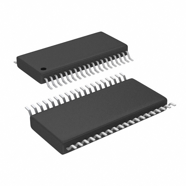


 工商网监
湘ICP备2023018690号
工商网监
湘ICP备2023018690号
