bq3285
Real-Time Clock (RTC)
Features
➤ Direct clock/calendar replacement for IBM® AT-compatible
computers and other applications
➤ Functionally compatible with the
DS1285
-
Closely matches MC146818A
pin configuration
➤ 114 bytes of general nonvolatile
storage
➤ 160ns cycle time allows fast bus
operation
➤ Calendar in day of the week, day
of the month, months, and years,
with automatic leap-year adjustment
➤ Time of day in seconds, minutes,
and hours
-
12- or 24-hour format
Optional daylight saving
adjustment
➤ Programmable square wave output
➤ Three individually maskable interrupt event flags:
➤ Selectable Intel or Motorola bus
timing
-
Periodic rates from 122µs to
500ms
➤ Less than 0.5µA load under battery operation
-
Time-of-day alarm once per
second to once per day
-
End-of-clock update cycle
➤ 14 bytes for clock/calendar and
control
General Description
The CMOS bq3285 is a low-power
microprocessor peripheral providing
a time-of-day clock and 100-year calendar with alarm features and battery operation. Other features include three maskable interrupt
sources, square wave output, and 114
bytes of general nonvolatile storage.
The bq3285 write-protects the clock,
calendar, and storage registers during
power failure. A backup battery
then maintains data and operates the
clock and calendar.
The bq3285 is a fully compatible
real-time clock for IBM AT compatible computers and other applications. The only external components are a 32.768kHz crystal and
a backup battery
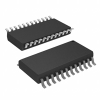
➤ 24-pin plastic DIP or SOIC
➤ BCD or binary format for clock
and calendar data
Pin Names
Pin Connections
MOT
X1
X2
AD0
AD1
AD2
AD3
AD4
AD5
AD6
AD7
VSS
1
2
3
4
5
6
7
8
9
10
11
12
24
23
22
21
20
19
18
17
16
15
14
13
VCC
SQW
NC
RCL
BC
INT
RST
DS
VSS
R/W
AS
CS
28-Pin PLCC No longer available
24-Pin DIP or SOIC
PN328501.eps
SLUS028A - JUNE 1991 - REVISED - MAY 2004
1
AD0–AD7
Multiplexed address/data
input/output
MOT
Bus type select input
CS
Chip select input
AS
Address strobe input
DS
Data strobe input
R/W
Read/write input
INT
Interrupt request
output
RST
Reset input
SQW
Square wave output
RCL
RAM clear input
BC
3V backup cell input
X1–X2
Crystal inputs
NC
No connect
VCC
+5V supply
VSS
Ground
�bq3285
Block Diagram
AD0–AD7
Pin Descriptions
MOT
Bus type select input
The bq3285 bus cycle consists of two
phases: the address phase and the datatransfer phase. The address phase precedes the data-transfer phase. During the
address phase, an address placed on
AD0–AD7 is latched into the bq3285 on the
falling edge of the AS signal. During the
data-transfer phase of the bus cycle, the
AD0–AD7 pins serve as a bidirectional data
bus.
MOT selects bus timing for either Motorola
or Intel architecture. This pin should be
tied to VCC for Motorola timing or to VSS for
Intel timing (see Table 1). The setting
should not be changed during system operation. MOT is internally pulled low by a
30KΩ resistor.
Table 1. Bus Setup
AS
Bus
Type
MOT
DS
R/W
AS
Level Equivalent Equivalent Equivalent
Motorola
VCC
DS, E, or
Φ2
R/W
Intel
VSS
RD,
MEMR, or
I/OR
WR,
MEMW, or ALE
I/OW
Multiplexed address/data input/
output
Address strobe input
AS serves to demultiplex the address/data
bus. The falling edge of AS latches the address on AD0–AD7. This demultiplexing process is independent of the CS signal. For
DIP a n d SOIC packages with MOT =
VCC, the AS input is provided a signal similar to ALE in an Intel-based system.
AS
2
�bq3285
DS
RCL
Data strobe input
When MOT = VCC, DS controls data transfer during a bq3285 bus cycle. During a
read cycle, the bq3285 drives the bus after
the rising edge on DS. During a write cycle,
the falling edge on DS is used to latch write
data into the chip.
A low level on the RCL pin causes the contents of each of the 114 storage bytes to be
set to FF(hex). The contents of the clock
and control registers are unaffected. This
pin should be used as a user-interface input
(pushbutton to ground) and not connected
to the output of any active component. RCL
input is only recognized when held low for
at least 125ms in the presence of VCC when
the oscillator is running. Using RAM clear
does not affect the battery load. This pin is
connected internally to a 30KΩ pull-up resistor.
When MOT = VSS, the DS input is provided
a signal similar to RD, MEMR, or I/OR in
an Intel-based system. The falling edge on
DS is used to enable the outputs during a
read cycle.
R/W
Read/write input
BC
When MOT = VCC, the level on R/W identifies the direction of data transfer. A high
level on R/W indicates a read bus cycle,
whereas a low on this pin indicates a write
bus cycle.
Upon power-up, a voltage within the VBC
range must be present on the BC pin for
the oscillator to start up.
Chip select input
CS should be driven low and held stable
during the data-transfer phase of a bus cycle accessing the bq3285.
INT
RST
Reset input
The bq3285 is reset when RST is pulled low.
When reset, INT becomes high-impedance,
and the bq3285 is not accessible. Table 4 in
the Control/Status Registers section lists
the register bits that are cleared by a reset.
Interrupt request output
INT is an open-drain output. INT is asserted low when any event flag is set and
the corresponding event enable bit is also
set. INT becomes high-impedance whenever
register C is read (see the Control/Status
Registers section).
SQW
3V backup cell input
BC should be connected to a 3V backup cell
for RTC operation and storage register nonvolatility in the absence of power. When
VCC slews down past VBC (3V typical), the
integral control circuitry switches the
power source to BC. When VCC returns
above VBC, the power source is switched to
VCC.
When MOT = VSS, R/W is provided a signal
similar to WR, MEMW, or I/OW in an Intelbased system. The rising edge on R/W
latches data into the bq3285.
CS
RAM clear input
Reset may be disabled by connecting RST
to VCC. This allows the control bits to reta i n th e i r s ta te s th ro u g h p o w erdown/power-up cycles.
Square-wave output
X1–X2
SQW may output a programmable frequency square-wave signal during normal
(VCC valid) system operation. Any one of
the 13 specific frequencies may be selected
through register A. This pin is held low
when the square-wave enable bit (SQWE)
in register B is 0 (see the Control/Status
Registers section).
Crystal inputs
The X1–X2 inputs are provided for an external 32.768Khz quartz crystal, Daiwa
DT-26 or equivalent, with 6pF load capacitance. A trimming capacitor may be necessary for extremely precise time-base generation.
In the absence of a crystal, an oscillated
output of 32.768kHz can be fed into the X1
input.
3
�bq3285
Functional Description
date period (see Figure 2). The alarm flag bit may also
be set during the update cycle.
Address Map
The bq3285 copies the local register updates into the
user buffer accessed by the host processor. When a 1 is
written to the update transfer inhibit bit (UTI) in register B, the user copy of the clock and calendar bytes remains unchanged, while the local copy of the same bytes
continues to be updated every second.
The bq3285 provides 14 bytes of clock and control/status
registers and 114 bytes of general nonvolatile storage.
Figure 1 illustrates the address map for the bq3285.
The update-in-progress bit (UIP) in register A is set
tBUC time before the beginning of an update cycle (see
Figure 2). This bit is cleared and the update-complete
flag (UF) is set at the end of the update cycle.
Update Period
The update period for the bq3285 is one second. The
bq3285 updates the contents of the clock and calendar
locations during the update cycle at the end of each up-
0
14
Bytes
13
14
114
Bytes
0
Seconds
00
1
Seconds Alarm
01
0D
2
Minutes
02
0E
3
Minutes Alarm
03
00
Clock and
Control Status
Registers
Storage
Registers
127
7F
4
Hours
04
5
Hours Alarm
05
6
Day of Week
06
7
Day of Month
07
8
Month
08
9
Year
09
10
Register A
0A
11
Register B
0B
12
Register C
0C
13
Register D
0D
BCD or
Binary
Format
Figure 1. Address Map
Update Period
(1s)
UIP
tUC (Update Cycle)
tBUC
Figure 2. Update Period Timing and UIP
4
�bq3285
c.
Programming the RTC
Write the appropriate value to the hour
format (HF) bit.
The time-of-day, alarm, and calendar bytes can be written in either the BCD or binary format (see Table 2).
2.
Write new values to all the time, alarm, and
calendar locations.
These steps may be followed to program the time, alarm,
and calendar:
3.
Clear the UTI bit to allow update transfers.
1.
On the next update cycle, the RTC updates all 10 bytes
in the selected format.
Modify the contents of register B:
a.
Write a 1 to the UTI bit to prevent transfers between RTC bytes and user buffer.
b.
Write the appropriate value to the data
format (DF) bit to select BCD or binary
format for all time, alarm, and calendar
bytes.
Table 2. Time, Alarm, and Calendar Formats
Range
Address
RTC Bytes
Decimal
Binary
Binary-Coded Decimal
0
Seconds
0–59
00H–3BH
00H–59H
1
Seconds alarm
0–59
00H–3BH
00H–59H
2
Minutes
0–59
00H–3BH
00H–59H
3
Minutes alarm
0–59
00H–3BH
00H–59H
Hours, 12-hour format
1–12
01H–OCH AM;
81H–8CH PM
01H–12H AM;
81H–92H PM
Hours, 24-hour format
0–23
00H–17H
00H–23H
Hours alarm, 12-hour format
1–12
01H–OCH AM;
81H–8CH PM
01H–12H AM;
81H–92H PM
Hours alarm, 24-hour format
0–23
00H–17H
00H–23H
6
Day of week (1=Sunday)
1–7
01H–07H
01H–07H
7
Day of month
1–31
01H–1FH
01H–31H
8
Month
1–12
01H–0CH
01H–12H
9
Year
0–99
00H–63H
00H–99H
4
5
5
�bq3285
The update-ended interrupt, which occurs at the end
of each update cycle
Square-Wave Output
n
The bq3285 divides the 32.768kHz oscillator frequency
to produce the 1Hz update frequency for the clock and
calendar. Thirteen taps from the frequency divider are
fed to a 16:1 multiplexer circuit. The output of this mux
is fed to the SQW output and periodic interrupt generation circuitry. The four least-significant bits of register
A, RS0–RS3, select among the 13 taps (see Table 3). The
square-wave output is enabled by writing a 1 to the
square-wave enable bit (SQWE) in register B.
Each of the three interrupt events is enabled by an individual interrupt-enable bit in register B. When an event
occurs, its event flag bit in register C is set. If the corresponding event enable bit is also set, then an interrupt
request is generated. The interrupt request flag bit
(INTF) of register C is set with every interrupt request.
Reading register C clears all flag bits, including INTF,
and makes INT high-impedance.
Two methods can be used to process bq3285 interrupt
events:
Interrupts
n
The bq3285 allows three individually selected interrupt
events to generate an interrupt request. These three interrupt events are:
n
n
n
The periodic interrupt, programmable to occur once
every 122µs to 500ms
Enable interrupt events and use the interrupt request
output to invoke an interrupt service routine.
Do not enable the interrupts and use a polling routine
to periodically check the status of the flag bits.
The individual interrupt sources are described in detail
in the following sections.
The alarm interrupt, programmable to occur once per
second to once per day
Table 3. Square-Wave Frequency/Periodic Interrupt Rate
Register A Bits
Square Wave
RS3
RS2
RS1
RS0
Frequency
0
0
0
0
None
0
0
0
1
256
Hz
3.90625
ms
0
0
1
0
128
Hz
7.8125
ms
0
0
1
1
8.192
kHz
122.070
µs
0
1
0
0
4.096
kHz
244.141
µs
0
1
0
1
2.048
kHz
488.281
µs
0
1
1
0
1.024
kHz
976.5625
0
1
1
1
512
Hz
1.95315
ms
1
0
0
0
256
Hz
3.90625
ms
1
0
0
1
128
Hz
7.8125
ms
1
0
1
0
64
Hz
15.625
ms
1
0
1
1
32
Hz
31.25
ms
1
1
0
0
16
Hz
62.5
ms
1
1
0
1
8
Hz
125
ms
1
1
1
0
4
Hz
250
ms
1
1
1
1
2
Hz
500
ms
6
Units
Periodic Interrupt
Period
Units
None
µs
�bq3285
Periodic Interrupt
Update Cycle Interrupt
The mux output used to drive the SQW output also
drives the interrupt-generation circuitry. If the periodic
interrupt event is enabled by writing a 1 to the periodic
interrupt enable bit (PIE) in register C, an interrupt request is generated once every 122µs to 500ms. The period between interrupts is selected by the same bits in
register A that select the square wave frequency (see Table 3).
The update cycle ended flag bit (UF) in register C is set
to a 1 at the end of an update cycle. If the update interrupt enable bit (UIE) of register B is 1, and the update
transfer inhibit bit (UTI) in register B is 0, then an interrupt request is generated at the end of each update
cycle.
Accessing RTC bytes
Alarm Interrupt
Time and calendar bytes read during an update cycle
may be in error. Three methods to access the time and
calendar bytes without ambiguity are:
During each update cycle, the RTC compares the hours,
minutes, and seconds bytes with the three corresponding
alarm bytes. If a match of all bytes is found, the alarm
interrupt event flag bit, AF in register C, is set to 1. If
the alarm event is enabled, an interrupt request is generated.
n
An alarm byte may be removed from the comparison by
setting it to a “don’t care” state. An alarm byte is set to
a “don’t care” state by writing a 1 to each of its two
most-significant bits. A “don’t care” state may be used to
select the frequency of alarm interrupt events as follows:
n
n
n
n
n
n
If none of the three alarm bytes is “don’t care,” the
frequency is once per day, when hours, minutes, and
seconds match.
If only the hour alarm byte is “don’t care,” the
frequency is once per hour, when minutes and
seconds match.
Enable the update interrupt event to generate
interrupt requests at the end of the update cycle.
The interrupt handler has a maximum of 999ms to
access the clock bytes before the next update cycle
begins (see Figure 3).
Poll the update-in-progress bit (UIP) in register A. If
UIP = 0, the polling routine has a minimum of tBUC
time to access the clock bytes (see Figure 3).
Use the periodic interrupt event to generate
interrupt requests every tPI time, such that UIP = 1
always occurs between the periodic interrupts. The
interrupt handler has a minimum of tPI/2 + tBUC
time to access the clock bytes (see Figure 3).
Oscillator Control
If only the hour and minute alarm bytes are “don’t
care,” the frequency is once per minute, when seconds
match.
When power is first applied to the bq3285 and VCC is
above VPFD, the internal oscillator and frequency divider
are turned on by writing a 010 pattern to bits 4 through
6 of register A. A pattern of 11X turns the oscillator on,
but keeps the frequency divider disabled. Any other pattern to these bits keeps the oscillator off.
If the hour, minute, and second alarm bytes are
“don’t care,” the frequency is once per second.
Figure 3. Update-Ended/Periodic Interrupt Relationship
7
�bq3285
RS0–RS3 - Frequency Select
Power-Down/Power-Up Cycle
7
-
The bq3285 continuously monitors V CC for out-oftolerance. During a power failure, when VCC falls below
VPFD (4.17V typical), the bq3285 write-protects the clock
and storage registers. When VCC is below VBC (3V typical), the power source is switched to BC. RTC operation
and storage data are sustained by a valid backup energy
source. When VCC is above VBC, the power source is VCC.
Write-protection continues for tCSR time after VCC rises
above VPFD.
7
-
2
RS2
1
RS1
0
RS0
6
OS2
5
OS1
4
OS0
3
-
2
-
1
-
0
-
UIP - Update Cycle Status
Register A Bits
5
4
3
2
OS1 OS0
RS3
RS2
1
RS1
0
RS0
7
UIP
Register A programs:
n
3
RS3
These three bits control the state of the oscillator and
divider stages. A pattern of 010 enables RTC operation
by turning on the oscillator and enabling the frequency
divider. A pattern of 11X turns the oscillator on, but
keeps the frequency divider disabled. When 010 is written, the RTC begins its first update after 500ms.
Register A
n
4
-
OS0–OS2 - Oscillator Control
The four control/status registers of the bq3285 are accessible regardless of the status of the update cycle (see Table 4).
6
OS2
5
-
These bits select one of the 13 frequencies for the SQW output and the periodic interrupt rate, as shown in Table 3.
Control/Status Registers
7
UIP
6
-
6
-
5
-
4
-
3
-
2
-
1
-
0
-
This read-only bit is set prior to the update cycle. When
UIP equals 1, an RTC update cycle may be in progress.
UIP is cleared at the end of each update cycle. This bit
is also cleared when the update transfer inhibit (UTI)
bit in register B is 1.
The frequency of the square-wave and the periodic
event rate.
Oscillator operation.
Register A provides:
n
Status of the update cycle.
Table 4. Control/Status Registers
Reg.
Loc.
(Hex) Read Write
Bit Name and State on Reset
7 (MSB)
6
5
4
3
1
UIP
na OS2 na OS1 na OS0 na
2
1
0 (LSB)
A
0A
Yes
Yes
B
0B
Yes
Yes
UTI
na
PIE
0
AIE
0
UIE
0
SQWE
0
DF
na
HF
na
C
0C
Yes
No
INTF
0
PF
0
AF
0
UF
0
-
0
-
0
-
0
-
0
D
0D
Yes
No
VRT
na
-
0
-
0
-
0
-
0
-
0
-
0
-
0
Notes:
1. Except bit 7.
2. na = not affected
8
RS3
na RS2 na RS1 na
RS0
na
DSE na
�bq3285
SQWE - Square-Wave Enable
Register B
7
UTI
6
PIE
5
AIE
Register B Bits
4
3
2
UIE SQWE DF
1
HF
7
-
0
DSE
6
-
5
-
4
-
3
SQWE
2
-
1
-
0
-
1
-
0
-
This bit enables the square-wave output:
1 = Enabled
Register B enables:
n
Update cycle transfer operation
n
Square-wave output
n
Interrupt events
n
Daylight saving adjustment
0 = Disabled and held low
UIE - Update Cycle Interrupt Enable
7
-
Register B selects:
n
6
-
All bits of register B are read/write.
1 = Enabled
DSE - Daylight Saving Enable
0 = Disabled
6
-
5
-
4
-
3
-
4
UIE
3
-
2
-
This bit enables an interrupt request due to an update
ended interrupt event:
Clock and calendar data formats
7
-
5
-
2
-
1
-
The UIE bit is automatically cleared when the UTI bit
equals 1.
0
DSE
AIE - Alarm Interrupt Enable
This bit enables daylight-saving time adjustments when
written to 1:
n
n
This bit enables an interrupt request due to an alarm
7
6
5
4
3
2
1
0
AIE
-
On the last Sunday in October, the first time the
bq3285 increments past 1:59:59 AM, the time falls
back to 1:00:00 AM.
interrupt event:
On the first Sunday in April, the time springs
forward from 2:00:00 AM to 3:00:00 AM.
1 = Enabled
0 = Disabled
HF - Hour Format
7
-
6
-
5
-
4
-
3
-
2
-
1
HF
PIE - Periodic Interrupt Enable
0
-
This bit enables an interrupt request due to a periodic
7
-
This bit selects the time-of-day and alarm hour format:
6
PIE
1 = 24-hour format
0 = 12-hour format
interrupt event:
1 = Enabled
DF - Data Format
7
-
6
-
5
-
4
-
3
-
2
DF
1
-
0 = Disabled
0
-
This bit selects the numeric format in which the time,
alarm, and calendar bytes are represented:
1 = Binary
0 = BCD
9
5
-
4
-
3
-
2
-
1
-
0
-
�bq3285
This bit is set to a 1 every tPI time, where tPI is the time
period selected by the settings of RS0–RS3 in register A.
Reading register C clears this bit.
UTI - Update Transfer Inhibit
7
UTI
6
-
5
-
4
-
3
-
2
-
1
-
0
-
INTF - Interrupt Request Flag
7
INTF
This bit inhibits the transfer of RTC bytes to the user
buffer:
1 = Inhibits transfer and clears UIE
Register C Bits
5
4
3
AF
UF
0
2
-
1
-
0
-
UIE = 1 and UF = 1
2
0
1
0
Reading register C clears this bit.
0
0
Register D
7
VRT
Bits 0–3 - Unused Bits
6
-
3
-
PIE = 1 and PF = 1
Register C is the read-only event status register.
7
-
4
-
AIE = 1 and AF = 1
Register C
6
PF
5
-
This flag is set to a 1 when any of the following is true:
0 = Allows transfer
7
INTF
6
-
5
-
4
-
3
0
2
0
1
0
6
-
5
-
4
-
3
-
2
-
1
-
0
-
Register D is the read-only data integrity status register.
0
0
Bits 0–6 - Unused Bits
These bits are always set to 0.
7
-
UF - Update Event Flag
7
-
6
-
5
-
4
UF
3
-
2
-
1
-
0
-
AF - Alarm Event Flag
6
-
5
AF
4
-
3
-
2
-
1
-
0
-
5
-
4
-
3
-
2
-
1
-
3
0
2
0
1
0
0
0
6
0
5
0
Register D Bits
4
3
0
0
2
0
1
0
0
0
1 = Valid backup energy source
0 = Backup energy source is depleted
When the backup energy source is depleted (VRT = 0),
data integrity of the RTC and storage registers is not
guaranteed.
PF - Periodic Event Flag
6
PF
4
0
VRT - Valid RAM and Time
7
VRT
This bit is set to a 1 when an alarm event occurs. Reading register C clears this bit.
7
-
5
0
These bits are always set to 0.
This bit is set to a 1 at the end of the update cycle.
Reading register C clears this bit.
7
-
6
0
0
-
10
�bq3285
Absolute Maximum Ratings
Symbol
Parameter
Value
Unit
Conditions
VCC
DC voltage applied on VCC relative to VSS
-0.3 to 7.0
V
VT
DC voltage applied on any pin excluding VCC
relative to VSS
-0.3 to 7.0
V
VT ≤ VCC + 0.3
TOPR
Operating temperature
0 to +70
°C
Commercial
TSTG
Storage temperature
-55 to +125
°C
TBIAS
Temperature under bias
-40 to +85
°C
TSOLDER
Soldering temperature
260
°C
Note:
For 10 seconds
Permanent device damage may occur if Absolute Maximum Ratings are exceeded. Functional operation should be limited to the Recommended DC Operating Conditions detailed in this data sheet. Exposure to conditions beyond the operational limits for extended periods of time may affect device reliability.
Recommended DC Operating Conditions (TA = TOPR)
Symbol
Parameter
Minimum
Typical
Maximum
Unit
VCC
Supply voltage
4.5
5.0
5.5
V
VSS
Supply voltage
0
0
0
V
VIL
Input low voltage
-0.3
-
0.8
V
VIH
Input high voltage
2.2
-
VCC + 0.3
V
VBC
Backup cell voltage
2.5
-
4.0
V
Note:
Typical values indicate operation at TA = 25°C.
11
�bq3285
DC Electrical Characteristics (TA = TOPR, VCC = 5V ± 10%)
Symbol
Parameter
Minimum
Typical
Maximum
Unit
Conditions/Notes
ILI
Input leakage current
-
-
±1
µA
VIN = VSS to VCC
ILO
Output leakage current
-
-
±1
µA
AD0–AD7, INT, and SQW
in high impedance,
VOUT = VSS to VCC
VOH
Output high voltage
2.4
-
-
V
IOH = -2.0 mA
VOL
Output low voltage
-
-
0.4
V
IOL = 4.0 mA
ICC
Operating supply current
-
7
15
mA
VSO
Supply switch-over voltage
-
VBC
-
V
ICCB
Battery operation current
-
0.3
0.5
µA
VPFD
Power-fail-detect voltage
4.0
4.17
4.35
V
IRCL
Input current when RCL = VSS.
-
-
185
µA
Internal 30K pull-up
IMOTH
Input current when MOT = VCC
-
-
-185
µA
Internal 30K pull-down
Notes:
Min. cycle, duty = 100%,
IOH = 0mA, IOL = 0mA
VBC = 3V, TA = 25°C
Typical values indicate operation at TA = 25°C, VCC = 5V or VBC = 3V.
Crystal Specifications (DT-26 or Equivalent)
Symbol
Parameter
Minimum
Typical
Maximum
Unit
fO
Oscillation frequency
-
32.768
-
kHz
CL
Load capacitance
-
6
-
pF
TP
Temperature turnover point
20
25
30
°C
k
Parabolic curvature constant
-
-
-0.042
ppm/°C
Q
Quality factor
40,000
70,000
-
R1
Series resistance
-
-
45
KΩ
C0
Shunt capacitance
-
1.1
1.8
pF
C0/C1
Capacitance ratio
-
430
600
DL
Drive level
-
-
1
µW
∆f/fO
Aging (first year at 25°C)
-
1
-
ppm
12
�bq3285
Capacitance (TA = 25°C, F = 1MHz, VCC = 5.0V)
Symbol
Parameter
Minimum
Typical
Maximum
Unit
Conditions
CI/O
Input/output capacitance
-
-
7
pF
VOUT = 0V
CIN
Input capacitance
-
-
5
pF
VIN = 0V
AC Test Conditions
Parameter
Test Conditions
Input pulse levels
0 to 3.0 V
Input rise and fall times
5 ns
Input and output timing reference levels
1.5 V (unless otherwise specified)
Output load (including scope and jig)
See Figures 4 and 5
Figure 4. Output Load A
Figure 5. Output Load B
13
�bq3285
Read/Write Timing (TA = TOPR, VCC = 5V ± 10%)
Symbol
Parameter
Minimum
Typical
Maximum
Unit
tCYC
Cycle time
160
-
-
ns
tDSL
DS low or RD/WR high time
80
-
-
ns
tDSH
DS high or RD/WR low time
55
-
-
ns
tRWH
R/W hold time
0
-
-
ns
tRWS
R/W setup time
10
-
-
ns
tCS
Chip select setup time
5
-
-
ns
tCH
Chip select hold time
0
-
-
ns
tDHR
Read data hold time
0
-
25
ns
tDHW
Write data hold time
0
-
-
ns
tAS
Address setup time
20
-
-
ns
tAH
Address hold time
5
-
-
ns
tDAS
Delay time, DS to AS rise
10
-
-
ns
tASW
Pulse width, AS high
30
-
-
ns
tASD
Delay time, AS to DS rise (RD/WR
fall)
35
-
-
ns
tOD
Output data delay time from DS rise
(RD fall)
-
-
50
ns
tDW
Write data setup time
30
-
-
ns
tBUC
Delay time before update cycle
-
244
-
µs
tPI
Periodic interrupt time interval
-
-
-
-
tUC
Time of update cycle
-
1
-
µs
14
Notes
See Table 3
�bq3285
Motorola Bus Read/Write Timing
15
�bq3285
Intel Bus Read Timing
Intel Bus Write Timing
16
�bq3285
Power-Down/Power-Up Timing (TA = TOPR)
Minimum
Typical
Maximum
Unit
tF
Symbol
VCC slew from 4.5V to 0V
Parameter
300
-
-
µs
tR
VCC slew from 0V to 4.5V
100
-
-
µs
tCSR
CS at VIH after power-up
20
-
200
ms
Power-Down/Power-Up Timing
17
Conditions
Internal write-protection
period after VCC passes VPFD
on power-up.
�bq3285
Interrupt Delay Timing (TA = TOPR)
Symbol
Parameter
Minimum
Typical
Maximum
Unit
tRSW
Reset pulse width
5
-
-
µs
tIRR
INT release from RST
-
-
2
µs
tIRD
INT release from DS (RD)
-
-
2
µs
Interrupt Delay Timing
18
�bq3285
24-Pin DIP (P)
24-Pin DIP (P)
Dimension
A
A1
B
B1
C
D
E
E1
e
G
L
S
Minimum
0.160
0.015
0.015
0.045
0.008
1.240
0.600
0.530
0.600
0.090
0.115
0.070
Maximum
0.190
0.040
0.022
0.065
0.013
1.280
0.625
0.570
0.670
0.110
0.150
0.090
All dimensions are in inches.
24-Pin SOIC (S)
24-Pin SOIC (S)
Dimension
A
A1
B
C
D
E
e
H
L
Minimum
0.095
0.004
0.013
0.008
0.600
0.290
0.045
0.395
0.020
All dimensions are in inches.
19
Maximum
0.105
0.012
0.020
0.013
0.615
0.305
0.055
0.415
0.040
�bq3285
Data Sheet Revision History
Change
No.
Page
No.
Description
Nature of Change
1
2
Address strobe input
Clarification
1
11
Backup cell voltage VBC
Was 2.0 min; is 2.5 min
1
12
Was 4.1 min, 4.25 max; in 4.0 mi, 4.35 max
2
3, 12
Power-fail detect voltage VPFD
crystal type Daiwa DT - 26 (not DT-26S)
3
12
Changed value in first table
IRCL max. was 275; is now 185
3
12
Changed value in first table
IMOTH max. was - 275; is now - 185
3
12
Changed values for conditions of IRCL, IMOTH
Was 20K; is now 30K
4
1, 8, 20
PLCC last time buy and Reg A update
Reg A labeling corrected
5
1, 8, 20
PLCC package option removed
PLCC reached end of Last Time Buy
Note:
Clarification
Change 1 = Nov. 1992 B changes from June 1991 A.
Change 2 = Nov. 1993 C changes from Nov. 1992 B
Change 3 = Sept. 1996 D changes from Nov. 1993 C
Change 4 = Jan. 1999 E changes from Sept. 1996 D
Change 5 = May 2004 (SLUS028A) changes from Jan. 1999 E
20
�bq3285
Ordering Information
bq3285
Temperature:
blank = Commercial (0 to +70°C)
Package Option:
P = 24-pin plastic DIP (0.600)
S = 24-pin SOIC (0.300)
Device:
bq3285 Real-Time Clock with 114 bytes of
general storage
21
�MECHANICAL DATA
MPDI008 – OCTOBER 1994
N (R-PDIP-T**)
PLASTIC DUAL-IN-LINE PACKAGE
24 PIN SHOWN
A
24
13
0.560 (14,22)
0.520 (13,21)
1
12
0.060 (1,52) TYP
0.200 (5,08) MAX
0.610 (15,49)
0.590 (14,99)
0.020 (0,51) MIN
Seating Plane
0.100 (2,54)
0.021 (0,53)
0.015 (0,38)
0.125 (3,18) MIN
0.010 (0,25) M
PINS **
0°– 15°
0.010 (0,25) NOM
24
28
32
40
48
52
A MAX
1.270
(32,26)
1.450
(36,83)
1.650
(41,91)
2.090
(53,09)
2.450
(62,23)
2.650
(67,31)
A MIN
1.230
(31,24)
1.410
(35,81)
1.610
(40,89)
2.040
(51,82)
2.390
(60,71)
2.590
(65,79)
DIM
4040053 / B 04/95
NOTES: A.
B.
C.
D.
All linear dimensions are in inches (millimeters).
This drawing is subject to change without notice.
Falls within JEDEC MS-011
Falls within JEDEC MS-015 (32 pin only)
POST OFFICE BOX 655303
• DALLAS, TEXAS 75265
�PACKAGE OPTION ADDENDUM
www.ti.com
10-Dec-2020
PACKAGING INFORMATION
Orderable Device
Status
(1)
Package Type Package Pins Package
Drawing
Qty
Eco Plan
(2)
Lead finish/
Ball material
MSL Peak Temp
Op Temp (°C)
Device Marking
(3)
(4/5)
(6)
BQ3285S-SB2
ACTIVE
SOIC
DW
24
25
RoHS & Green
NIPDAU
Level-1-260C-UNLIM
0 to 70
3285S
-SB2
(1)
The marketing status values are defined as follows:
ACTIVE: Product device recommended for new designs.
LIFEBUY: TI has announced that the device will be discontinued, and a lifetime-buy period is in effect.
NRND: Not recommended for new designs. Device is in production to support existing customers, but TI does not recommend using this part in a new design.
PREVIEW: Device has been announced but is not in production. Samples may or may not be available.
OBSOLETE: TI has discontinued the production of the device.
(2)
RoHS: TI defines "RoHS" to mean semiconductor products that are compliant with the current EU RoHS requirements for all 10 RoHS substances, including the requirement that RoHS substance
do not exceed 0.1% by weight in homogeneous materials. Where designed to be soldered at high temperatures, "RoHS" products are suitable for use in specified lead-free processes. TI may
reference these types of products as "Pb-Free".
RoHS Exempt: TI defines "RoHS Exempt" to mean products that contain lead but are compliant with EU RoHS pursuant to a specific EU RoHS exemption.
Green: TI defines "Green" to mean the content of Chlorine (Cl) and Bromine (Br) based flame retardants meet JS709B low halogen requirements of


 工商网监
湘ICP备2023018690号
工商网监
湘ICP备2023018690号
