User's Guide
SLVU987 – January 2014
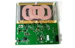
bq500412 bqTESLA Wireless Power TX EVM
The bqTESLA™ wireless power transmitter evaluation module from Texas Instruments is a highperformance, easy-to-use development module for the design of wireless power solutions. The bq500412
EVM evaluation module (EVM) provides all the basic functions of a Qi-compliant three coil, A6 type,
wireless charger pad. The EVM is intended to be used with bq51013BEVM-764 or any other Qi-compliant
receiver. Both the WPC 1.0 and WPC 1.1 receivers are supported with this design. The bq500412EVM584 is a 12-V input design with an optional boost convert for operation from 5-V input.
1
2
3
4
5
6
7
8
9
Contents
Applications .................................................................................................................. 2
bq500412EVM-550 Electrical Performance Specifications ............................................................ 2
Modifications ................................................................................................................. 2
Connector and Test Point Descriptions .................................................................................. 3
4.1
Input/Output Connections ......................................................................................... 3
4.2
Test Point Descriptions ............................................................................................ 3
Schematic and Bill of Materials ........................................................................................... 5
Test Setup .................................................................................................................. 10
6.1
Equipment ......................................................................................................... 10
6.2
Equipment Setup ................................................................................................. 11
bq500412EVM-584 Assembly Drawings and Layout ................................................................. 14
Reference ................................................................................................................... 19
FCC and IC Regulatory Compliance .................................................................................... 20
List of Figures
1
bq500412EVM-584 Schematic (1 of 2) ..................................................................................
2
bq500412EVM-584 Schematic (2 of 2) ..................................................................................
6
3
Equipment Setup ..........................................................................................................
11
4
Efficiency versus Power, bq500412EVM-584 Transmitter and HPA764 Receiver
...............................
Assembly Top ..............................................................................................................
Top Silk .....................................................................................................................
Top Layer ...................................................................................................................
Layer 2 ......................................................................................................................
Layer 3 ......................................................................................................................
Bottom Layer ...............................................................................................................
12
5
6
7
8
9
10
5
14
15
16
17
18
19
List of Tables
1
bq500412EVM-584 Electrical Performance Specifications ............................................................
2
2
Bill of Materials ..............................................................................................................
7
bqTESLA, Dynamic Power Limiting are trademarks of Texas Instruments.
Avid is a registered trademark of Avid Technology, Inc..
SLVU987 – January 2014
Submit Documentation Feedback
bq500412 bqTESLA Wireless Power TX EVM
Copyright © 2014, Texas Instruments Incorporated
1
�Applications
1
www.ti.com
Applications
The bq500412EVM-584 evaluation module demonstrates the transmitter portion of the bqTESLA™
wireless power system. This transmitter EVM is a complete transmitter-side solution that powers a
bqTESLA™ receiver. The EVM requires only input power for operation, 12 V at 1 A or 5 V at 2.5 A. All
transmitter-side electronics and transmitter coils are on a single 4-layer printed-circuit board (PCB). The
open design allows easy access to key points of the electrical schematic.
This EVM has the following features:
• WPC A6-Type transmitter coil, 70 mm × 25 mm free positioning area
• Input voltage 12 V or 5 V, using optional boost converter
• WPC 1.1 Foreign Object Detection (FOD) and WPC 1.0 Parasitic Metal Object Detection (PMOD)
• Dynamic Power Limiting™ (DPL) allows operation from a 5-V supply with limited current capability (for
example, a USB port)
• Reduced parts count from the legacy bq500410A design
• Compact power section design using the CSD97374 NexFET power stage
• LED indicates power transfer or power fault state
2
bq500412EVM-550 Electrical Performance Specifications
Table 1 provides a summary of the EVM performance specifications. All specifications are given for an
ambient temperature of 25°C.
Table 1. bq500412EVM-584 Electrical Performance Specifications
Parameter
Notes and Conditions
Min
Typ
Max
Unit
11.50
12.0
12.50
V
570
1000
mA
Input Characteristics
VIN
Input voltage
IIN
Input current
VIN = 12 V, RX IOUT = 1 A at 5 V
Input no-load current
VIN = 12 V, IOUT = 0 A
Input stand-by current
VIN = 12 V
72
mA
18.75
mA
Output Characteristics – Receiver bq51013BEVM-764
VOUT
IOUT
Output voltage
VIN = Nom, IOUT = Nom
Output ripple
VIN = Nom, IOUT = Max
4.5
5
5.1
V
200
mVPP
VIN = Min to Max
VIN = Min to Max
0
1
A
Output overcurrent
VIN = Nom
1
1.1
A
110
205
kHz
Systems Characteristics
3
FS
Switching frequency
Switching frequency varies with load
ηpk
Peak efficiency
VIN = 12 V, P Out RX = 2.5 W
73
%
η
Full-load efficiency
VIN = Nom, IOUT = Max
70
%
Modifications
See the datasheet (SLUSB026) when changing components.
Use LED mode – resistor R32 to change the behavior of the status LED, D6, D7 and D8. The standard
value is 42.2 kΩ for control option 1, see the datasheet for additional settings.
FOD threshold setting can be changed using R34. If R34 is removed then FOD function is disabled.
PMOD threshold setting can be changed using R35. If R35 is removed then PMOD function is disabled.
FOD_CAL can be used to change the slope of the FOD LOSS curve for better FOD performance, R33.
2
bq500412 bqTESLA Wireless Power TX EVM
Copyright © 2014, Texas Instruments Incorporated
SLVU987 – January 2014
Submit Documentation Feedback
�Connector and Test Point Descriptions
www.ti.com
4
Connector and Test Point Descriptions
4.1
Input/Output Connections
The connection points are described in Section 4.1.1 through Section 4.1.5.
4.1.1
J1 – VIN
Input power 12 V ±200 mV, return at J2.
4.1.2
J2 – GND
Return for input 12 V at J1.
J3 – Input Power 5 V ±100 mV, return at J4.
J4 – Return for 5 V input at J3
4.1.3
J6 –JTAG
Factory use only.
4.1.4
J7 – Serial Interface
Used with bqTESLA TX Tuning Tool Software for FOD set up.
4.1.5
J5 - Micro USB
Input power connector.
4.2
Test Point Descriptions
The test points are described in Section 4.2.1 through Section 4.2.15.
4.2.1
TP1 – DPWM Signal
Digital output signal from bq500412 to H-Bridge drive.
4.2.2
TP2 – I SENSE Signal
Input current-sense voltage, scale 1 V = 0.5 A.
4.2.3
TP3 – COMM + Signal
Sample of coil voltage for communications with RX.
4.2.4
TP4 – COMM - Signal
Sample of coil return for communications.
4.2.5
TP5 – Reserved
Reserved – no connection.
4.2.6
TP6 – Reserved
Reserved – no connection.
4.2.7
TP7 – V SENSE
Voltage sample of bridge voltage, divider ration 76.8 k / 10 k.
SLVU987 – January 2014
Submit Documentation Feedback
bq500412 bqTESLA Wireless Power TX EVM
Copyright © 2014, Texas Instruments Incorporated
3
�Connector and Test Point Descriptions
4.2.8
www.ti.com
TP8 – Buzzer AC Drive
Output from IC to drive AC buzzer, signals start of power transfer.
4.2.9
TP9 – Buzzer DC Drive
Output from IC to drive DC buzzer, signals start of power transfer.
4.2.10
TP10 - V-in
Sample voltage used for DPL, represents 5-V input.
4.2.11
TP11 – Analog Ground
Low-noise analog ground.
4.2.12
TP12 – Analog Ground
Low-noise analog ground
4.2.13
TP13 – Coil 1 Enable Drive
Output from bq500412, low enables coil 1 drive.
4.2.14
TP14 – Coil 2 Enable Drive
Output from bq500412, low enables coil 2 drive.
4.2.15
TP15 – Coil 3 Enable Drive
Output from bq500412, low enables coil 3 drive.
4
bq500412 bqTESLA Wireless Power TX EVM
Copyright © 2014, Texas Instruments Incorporated
SLVU987 – January 2014
Submit Documentation Feedback
�Schematic and Bill of Materials
www.ti.com
5
Schematic and Bill of Materials
This section includes the schematics and bill of materials for the EVM.
Figure 1 and Figure 2 illustrate the schematics for this EVM.
5V
R11
U4
TPS54231D
EN
C19 R4
10μF 3.60k
C8
0.1μF
J2
1
2
AGND
C4
47μF
1
TP7
2
V_SENSE
R2
3.16k
AGND
AGND
3
U3
INA199A1DCK
C11
0.1μF
R7
150k
4
2
3
AGND
AGND
GND
GND
AGND
C20
0.1μF
R5
1.00k
AGND
R67
10.0k
TP2
1
C50
0.033μF
3
R50
18.2k
AGND
D9
GRN
USB
4
R52
16.2k
J4
AGND
U5
TPS61087DSC
C38
22μF
5
COMP
SS
FB
FREQ
EN
IN
AGND
PGND
1
2
AGND
R69 TP10
76.8k
10
C39
0.068μF
9
V_IN
C51
0.033μF
8
SW
C28
4700 pF
R19
COMM+
AGND
6
SW
C52
0.1μF
TP3
R70
10.0k
7
10.0
L2
10μH
11
AGND
3
C48
22μF
R29
Vcc
22.0
C49
0.1μF
B2
GND
B1
Coil1.1
S
VCC
A
TP11
C9
R17
10.0k
L4
F
AGND
AGND
5
AGND
D11
AGND
C60
100μF
SNOOZE
C61
4.7μF
R28
R27 523k
523k
C25
4.7μF
D5
R76
10.0k
AGND
AGND
4
3
2
1
PWR_UP
EN
Q7
BSS138
AGND
PMOD
LED_A
LED_B
SLEEP
R23
475
AGND
V_IN
V_SENSE
I_SENSE
46
45
42
6
7
8
9
V33FB
ADCREF
RESET
PWR_UP
SNOOZE_CAP
T_SENSE
COIL_PEAK
V_IN
V_SENSE
I_SENSE
BPCAP
JTAG_TRST
JTAG_TMS
JTAG_TDI
JTAG_TDO
JTAG_TCK
RESERVED
RESERVED
DATA
CLK
U1
BQ500412A
PMOD
LED_A
LED_B
SLEEP
PWM_A
FOD
LOAD_FET
COIL1.1
COIL1.2
COIL1.3
35
31
30
29
28
27
10.0
/TRST
TMS
TDI
TDO
TCK
20
19
11
10
TP5
TP6
FOD_CAL
LED_A
R24
475
LED_B
R25
475
LED_C
COMM+
COMM-
R26
475
D6
GRN
PWR_UP
D7
RED
COMM_A+
COMM_ACOMM_B+
COMM_B-
COIL_SEL
LED_C
BUZ_DC
BUZ_AC
Net-Tie
D8
YLW
AGND
GND
AGND
Vcc
LED_MODE
LOSS_THR
2
B2
GND
B1
C43
0.068μF
C44
0.015μF
Q3
R13
100
26
25
24
23
C56
0.1μF
R56
10.0k
10.0
R73
10.0k
PMOD
FOD
FOD_CAL
R33
10.0k
R32
42.2k
C45
0.068μF
C55
4700pF
Coil1.3
1
2
3
B2
TP15
Vcc
GND
B1
S
VCC
A
6
5
R59 R60
200k 23.2k
C46
0.068μF
R61
C47
NoPop
Q4
R14
100
R39
10.0k
C26
1000 pF
GND
4
U8
SN74LVC1G3157DCKR
R34
86.6k
C54
33pF
Coil1.3
R58
44
43
R35
133k
1000 pF
GND
Vcc
LED_C
TP8
10.0k
L5
R72
NoPop
TP9
5
4
AGND
R31
3.60k
Coil1.1
Coil1.2
Coil1.3
A
F
DPWM
10.0
FOD
VCC
R38
R54 R55
200k 23.2k
C10
10.0
R30
12
13
14
15
16
17
S
R57
TP1
AGND
NT1
R49
1.0Meg
37
38
39
40
SNOOZE
SNOOZE_CHG
FOD_CAL
47
36
32
49
D2
18
21
22
GND
GND
GND
EPAD
SNOOZE
TP14
6
U7
SN74LVC1G3157DCKR
AGND
DATA
CLK
1
3
R15
10.0k
AGND
5V
C42
0.068μF
C53
4700pF
Coil1.2
Coil1.2
R53
AGND
V33A
41
48
C58
0.1μF
34
33
AGND
C29
4700pF
t°
NTC
C23
330pF
V33D
R64
2.00Meg
R65
392k
C24
1 μF
R68
10.0k
R22
3.01Meg
C21
33pF
4.7μF
C14 0.1μF
C16 0.1μF
10.0
1000 pF
GND
TP12
C15 4.7μF
R21
10.0k
10.0
COMM+
R71
10.0k
R16 R18
200k 23.2k
C13 1μF
AGND
C59
1 μF
R12
100
R37
4
R20
COMM-
Q2
C2
Coil1.1
6
5
C41
NoPop
C40
0.068μF
TP13
Vcc
U6
SN74LVC1G3157DCKR
TP4
D10
AGND
D4
2
Vin
AGND
5V
1
C22
4700pF
1,2,3
C37
22μF
5
SLEEP
F
1,2,3
C36
22μF
2
C30
2.2μF
L3
C27
0.1μF
1,2,3
R36
1.00k
C35
1 μF
4
R74
523k
GND
5,6,
7,8
C34
1 μF
3
Q6
BSS138
GND
5,6,
7,8
L7
2
R48
1.0Meg
C18
10μF
158k
PWPD
6
7
8
9
10
11
R75
10.0k
5
VIN
1 μF
C6
0.1μF
R51
1
R63
1.00k
R10 1.00
GND
AGND
Q5
DTC114YUAT-106
0.1μF
6
BOOT_R
AGND
J5
_
DPWM
7 C12
BOOT
PGND
VSW
8
PWM
VDD
Vcc
I_SENSE
5 Vin
SKIP#
C17
6
1
2
U2
CSD97374CQ4M
C7 1μF
C3
AGND
2700pF
AGND
R9
10.0
R66
76.8k
C5
0.1μF
R6
150k
D1
R3
76.8k
0.01μF
J3
+
BOOT
VSENSE
SS
COMP
GND
C31
D3
GRN
EN
4
6
0.1μF
Q1
5,6,
7,8
_
C33
1 μF
C1
1
5
R1
10.0k
9
C32
1 μF
12 Vin
3
0.04
R8
10.0
Vcc
47μH
8
PH
5
VIN
4
2
L6
7
+
Vin
L1
PGND
Vin
1
2
1
J1
R62
10.0k
C57
33pF
10.0
AGND
AGND
AGND
AGND
AGND
AGND
Figure 1. bq500412EVM-584 Schematic (1 of 2)
SLVU987 – January 2014
Submit Documentation Feedback
bq500412 bqTESLA Wireless Power TX EVM
Copyright © 2014, Texas Instruments Incorporated
5
�Schematic and Bill of Materials
www.ti.com
FID1
Vcc
PCB Number: PWR584
PCB Rev: A
R40
R41
R42
R43
R44
R45
R46
R47
10.0k 10.0k 10.0k 10.0k 10.0k 10.0k 10.0k 10.0k
TCK
FID2
FID3
TDO
LBL1
PCB Label
Size: 0.65" x0.20 "
PCB
LOGO
Texas Instruments
ZZ1
Label Assembly Note
This Assembly Note is for PCB labels only
H34
H35
2563
2563
H36
H37
2563
2563
H38
H39
H1
MECH
MCH004
H12
MECH
561-F440.5
H22
MECH
9911-187
H2
MECH
NY HN 440
H13
MECH
561-F440.5
H23
MECH
9911-187
H3
MECH
NY HN 440
H14
MECH
561-F440.5
H24
MECH
9911-187
H4
MECH
NY HN 440
H15
MECH
561-F440.5
H25
MECH
9911-187
H5
MECH
NY HN 440
H16
MECH
561-F440.5
H26
MECH
9911-187
H6
MECH
NY HN 440
H17
MECH
561-F440.5
H27
MECH
9911-187
H7
MECH
NY HN 440
H18
MECH
561-F440.25
H28
MECH
3348
H8
MECH
NY HN 440
H19
MECH
561-F440.25
H29
MECH
3348
H9
MECH
NY HN 440
H20
MECH
561-F440.25
H30
MECH
3348
H10
MECH
NY HN 440
H21
MECH
561-F440.25
H31
MECH
3348
TDI
/TRST
TMS
2563
ZZ2
Assembly Note
These assemblies are ESD sensitive, ESD precautions shall be observed.
ZZ3
Assembly Note
These assemblies must be clean and free from flux and all contaminants. Use of no clean flux is not acceptable.
ZZ4
Assembly Note
These assemblies must comply with workmanship standards IPC-A-610 Class 2., unless otherwise specified.
H11
MECH
NY HN 440
JTAG
10
8
6
4
2
9
7
5
3
1
CLK
DATA
2563
J6
14
13
12
11
10
9
8
7
6
5
4
3
2
1
For Development Only
J7
PMBUS
AGND
H32
MECH
3348
H33
MECH
3348
Figure 2. bq500412EVM-584 Schematic (2 of 2)
6
bq500412 bqTESLA Wireless Power TX EVM
SLVU987 – January 2014
Submit Documentation Feedback
Copyright © 2014, Texas Instruments Incorporated
�Schematic and Bill of Materials
www.ti.com
Table 2 contains the BOM for this EVM.
Table 2. Bill of Materials
Designator
Qty
Value
Description
Package
Reference
Part Number
Manufacturer
Alternate
Part Number
Alternate
Manufacturer
C1, C5, C6, C8, C11, C12,
C14, C16, C20, C27, C49,
C52, C56, C58
14
0.1uF
CAP, CERM, 0.1uF, 25V, +/-10%, X7R, 0603
0603
C1608X7R1E104K
TDK
C2, C10, C26
3
1000pF
CAP, CERM, 1000pF, 50V, +/-5%, COG/NPO, 0603
0603
C0603COGG1H102J080
TDK
C3
1
2700pF
CAP, CERM, 2700pF, 50V, +/-5%, C0G/NP0, 0603
0603
C1608C0G1H272J
TDK
C4
1
47uF
CAP, CERM, 47uF, 6.3V, +/-20%, X5R, 1206
1206
C3216X5R0J476M
TDK
C7, C13, C17, C24, C59
5
1uF
CAP, CERM, 1uF, 16V, +/-10%, X7R, 0603
0603
C1608X7R1C105K
TDK
C9, C15
2
4.7uF
CAP, CERM, 4.7uF, 6.3V, +/-20%, X5R, 0603
0603
C1608X5R0J475M
TDK
C18, C19
2
10uF
CAP, CERM, 10uF, 16V, +/-20%, X7R, 1210
1210
C3225X7R1C106M
TDK
C21, C54, C57
3
33pF
CAP, CERM, 33pF, 100V, +/-5%, C0G/NP0, 0603
0603
GRM1885C2A330JA01D
MuRata
C22, C28, C29, C53, C55
5
4700pF
CAP, CERM, 4700pF, 100V, +/-5%, C0G/NP0, 0805
0805
C2012C0G2A472J
TDK
C23
1
330pF
CAP, CERM, 330pF, 50V, +/-5%, C0G/NP0, 0603
0603
C1608C0G1H331J
TDK
C25
1
4.7uF
CAP, CERM, 4.7uF, 10V, +/-20%, X7R, 0805
0805
C2012X7R1A475M
TDK
C30
1
2.2uF
CAP, CERM, 2.2uF, 10V, +/-10%, X7R, 0603
0603
GRM188R71A225KE15D
MuRata
C31
1
0.01uF
CAP, CERM, 0.01uF, 25V, +/-5%, C0G/NP0, 0603
0603
C1608C0G1E103J
TDK
C32, C33, C34, C35
4
1uF
CAP, CERM, 1uF, 25V, +/-10%, X7R, 1206
1206
C3216X7R1E105K
TDK
C36, C37, C38
3
22uF
CAP, CERM, 22uF, 16V, +/-20%, X5R, 1210
1210
C3225X5R1C226M
TDK
C39, C40, C42, C43, C45,
C46
6
0.068uF
CAP, CERM, 0.068uF, 50V, +/-5%, C0G/NP0, 1206
1206
GRM31C5C1H683JA01L
MuRata
C3216C0G1H683J160AA
TDK
C44
1
0.015uF
CAP, CERM, 0.015uF, 50V, +/-5%, C0G/NP0, 1206
1206
C48
1
22uF
CAP, CERM, 22uF, 16V, +/-20%, X7R, 1210
1210
GRM3195C1H153JA01D
MuRata
C3216C0G1H153J060AA
TDK
C3225X7R1C226M
TDK
C50, C51
2
0.033uF
CAP, CERM, 0.033uF, 25V, +/-10%, X7R, 0603
C60
1
100uF
CAP, CERM, 100uF, 6.3V, +/-20%, X5R, 1210
0603
GRM188R71E333KA01D
MuRata
1210
GRM32ER60J107ME20L
C61
1
4.7uF
MuRata
CAP, CERM, 4.7uF, 16V, +/-10%, X5R, 0805
0805
GRM219R61C475KE15D
D1
1
MuRata
0.51V
Diode, Schottky, 40V, 0.5A, SOD-123
SOD-123
MBR0540T1G
ON
Semiconductor
D2, D4, D5, D11
D3, D6, D9
4
BAV21WS
Diode, SMD Switching, 200mA, 200V
SOD-323
BAV21WS-7-F
Diodes
3
GRN
LED, Green, SMD
1.6x0.8x0.8mm
LTST-C190GKT
Lite-On
D7
1
RED
LED, Red, SMD
1.6x0.8x0.8mm
LTST-C190KRKT
Lite-On
D8
1
YLW
LED, Yellow, SMD
1.6x0.8x0.8mm
LTST-C191KSKT
Lite-On
D10
1
LS22-E3
Diode, Schottky Rectifier, 2A, 20 V
DO-214AA
LS22-E3
Vishay
L1
1
47uH
Inductor, Shielded Drum Core, Ferrite, 47uH, 0.25A, 0.94
ohm, SMD
WE-TPC-S
744031470
Wurth Elektronik
eiSos
L2
1
10uH
Inductor, Shielded Drum Core, Ferrite, 10uH, 1.83A, 0.064
ohm, SMD
WE-PD-S
744778910
Wurth Elektronik
eiSos
L3, L4, L5
1
12.5uH
Coil Assembly WPC type A6, Triple coil (L3,L4,L5)
53 mm x 130 mm
760-308-106
Wurth Elektronik
L6, L7
2
Choke
Inductor, CMC Toroid, 1.5A, 60milliohm
0.197 X 0.197 inch
DLW5BSN102SQ2L
muRata
NTC
1
10.0k ohm
Thermistor NTC, 10.0k ohm, 1%, 0603
0603
NTCG163JF103F
TDK
-
-
Q1
1
0.7V
Transistor, NPN, 45V, 0.1A, SOT-23
SOT-23
BC847CLT1G
ON
Semiconductor
None
None
SLVU987 – January 2014
Submit Documentation Feedback
bq500412 bqTESLA Wireless Power TX EVM
Copyright © 2014, Texas Instruments Incorporated
7
�Schematic and Bill of Materials
www.ti.com
Table 2. Bill of Materials (continued)
Designator
Qty
Value
Description
Package
Reference
Part Number
Manufacturer
Q2, Q3, Q4
3
MOSFET 60V
MOSFET, N-CH, 60V, 22A, SON 3.3x3.3mm
SON 3.3x3.3mm
FDMC86520L
Fairchild
Semiconductor
Q5
1
DTC114YUA
Transistor, Digital NPN, 50 V, 100 mA
SC-70
DTC114YUAT-106
Rohm
Q6, Q7
2
50V
MOSFET, N-CH, 50V, 0.22A, SOT-23
SOT-23
BSS138
Fairchild
Semiconductor
R1, R15, R17, R33, R37,
R38, R39, R40, R41, R42,
R43, R44, R45, R46, R47,
R56, R62, R67, R68, R70,
R71, R73, R75, R76
24
10.0k
RES, 10.0k ohm, 1%, 0.1W, 0603
0603
RC0603FR-0710KL
Yageo America
R2
1
3.16k
RES, 3.16k ohm, 1%, 0.1W, 0603
0603
RC0603FR-073K16L
Yageo America
R3, R66, R69
3
76.8k
RES, 76.8k ohm, 1%, 0.1W, 0603
0603
RC0603FR-0776K8L
Yageo America
R4, R31
2
3.60k
RES, 3.60k ohm, 1%, 0.1W, 0603
0603
RC0603FR-073K6L
Yageo America
R5, R36, R63
3
1.00k
RES, 1.00k ohm, 1%, 0.1W, 0603
0603
RC0603FR-071KL
Yageo America
R6, R7
2
150k
RES, 150k ohm, 1%, 0.1W, 0603
0603
RC0603FR-07150KL
Yageo America
R8, R9, R19, R20, R21,
R30, R53, R57, R58, R61
10
10.0
RES, 10.0 ohm, 1%, 0.1W, 0603
0603
RC0603FR-0710RL
Yageo America
R10
1
1.00
RES, 1.00 ohm, 1%, 0.1W, 0603
0603
RC0603FR-071RL
Yageo America
R11
1
0.04
RES, 0.04 ohm, 1%, 1W, 2010
2010
CSRN2010FK40L0
Stackpole
Electronics Inc
R12, R13, R14
3
100
RES, 100 ohm, 1%, 0.1W, 0603
0603
CRCW0603100RFKEA
Vishay-Dale
R16, R54, R59
3
200k
RES, 200k ohm, 1%, 0.1W, 0603
0603
RC0603FR-07200KL
Yageo America
R18, R55, R60
3
23.2k
RES, 23.2k ohm, 1%, 0.1W, 0603
0603
RC0603FR-0723K2L
Yageo America
R22
1
3.01Meg
RES, 3.01Meg ohm, 1%, 0.1W, 0603
0603
RC0603FR-073M01L
Yageo America
R23, R24, R25, R26
4
475
RES, 475 ohm, 1%, 0.1W, 0603
0603
RC0603FR-07475RL
Yageo America
R27, R28, R74
3
523k
RES, 523k ohm, 1%, 0.1W, 0603
0603
RC0603FR-07523KL
Yageo America
R29
1
22.0
RES, 22.0 ohm, 1%, 0.1W, 0603
0603
RC0603FR-0722RL
Yageo America
R32
1
42.2k
RES, 42.2k ohm, 1%, 0.1W, 0603
0603
RC0603FR-0742K2L
Yageo America
R34
1
86.6k
RES, 86.6k ohm, 1%, 0.1W, 0603
0603
RC0603FR-0786K6L
Yageo America
R35
1
133k
RES, 133k ohm, 1%, 0.1W, 0603
0603
RC0603FR-07133KL
Yageo America
R48, R49
2
1.0Meg
RES, 1.0Meg ohm, 5%, 0.1W, 0603
0603
CRCW06031M00JNEA
Vishay-Dale
R50
1
18.2k
RES, 18.2k ohm, 1%, 0.1W, 0603
0603
RC0603FR-0718K2L
Yageo America
R51
1
158k
RES, 158k ohm, 1%, 0.1W, 0603
0603
RC0603FR-07158KL
Yageo America
R52
1
16.2k
RES, 16.2k ohm, 1%, 0.1W, 0603
0603
RC0603FR-0716K2L
Yageo America
R64
1
2.00Meg
RES, 2.00Meg ohm, 1%, 0.1W, 0603
0603
RC0603FR-072ML
Yageo America
R65
1
392k
RES, 392k ohm, 1%, 0.1W, 0603
0603
RC0603FR-07392KL
Yageo America
U1
1
BQ500412RGZ
IC, Qi Compliant Wireless Power Transmitter Manager
VQFN
BQ500412RGZ
TI
None
U2
1
CSD97374CQ4M
IC, Synchronous Buck NexFETPower Stage
QFN
CSD97374CQ4M
TI
None
U3
1
Voltage Output, High or Low Side Measurement, BiDirectional Zerø-Drift Series Current-Shunt Monitor,
DCK0006A
DCK0006A
INA199A1DCK
TI
None
U4
1
Buck Step Down Regulator with 3.5 to 28 V Input and 0.8 to
25 V Output, -40 to 150 degC, 8-Pin SOIC (D), Green (RoHS
& no Sb/Br)
D0008A
TPS54231D
TI
8
bq500412 bqTESLA Wireless Power TX EVM
Alternate
Part Number
Alternate
Manufacturer
None
None
Equivalent
None
SLVU987 – January 2014
Submit Documentation Feedback
Copyright © 2014, Texas Instruments Incorporated
�Schematic and Bill of Materials
www.ti.com
Table 2. Bill of Materials (continued)
Designator
Qty
Value
Description
Package
Reference
Part Number
Manufacturer
U5
1
TPS61087DSC
IC, 600kHz/1.2MHz Step-Up DC-Dc Converter
SON-10
TPS61087DSC
TI
None
U6, U7, U8
3
SN74LVC1G3157DCKR
IC, SPDT Analog Switch
SC-70
SN74LVC1G3157DCKR
TI
None
C41, C47
0
NoPop
CAP, CERM,
1206
R72
0
NoPop
RES,
0603
SLVU987 – January 2014
Submit Documentation Feedback
Alternate
Part Number
Alternate
Manufacturer
bq500412 bqTESLA Wireless Power TX EVM
Copyright © 2014, Texas Instruments Incorporated
9
�Test Setup
6
Test Setup
6.1
Equipment
6.1.1
www.ti.com
bqTESLA™ Receiver
Use the bq51013BEVM-764 or a Qi-compliant receiver to work with this EVM.
6.1.2
Voltage Source
The input voltage source must provide a regulated DC voltage of 12 V and deliver at least 1-A continuous
load current; current limit must be set to 2 A. If 5 V is used, the current should be 2.5 A with a current limit
of 3 A.
CAUTION
To help assure safety and integrity of the system and minimize risk of electrical
shock hazard, always use a power supply providing suitable isolation and
supplemental insulation (double insulated). Compliance to IEC 61010-1, Safety
Requirements for Electrical Equipment for Measurement, Control and
Laboratory Use, Part 1, General Requirements, or its equivalent is strongly
suggested, including any required regional regulatory compliance certification
approvals. Always select a power source that is suitably rated for use with this
EVM as referenced in this user manual.
External Power Supply Requirements:
Nom Voltage: 12.0 VDC
Max Current: 2.0 A
Efficiency Level V
Or:
Nom Voltage: 5.0 VDC
Max Current: 3.0 A
Efficiency Level V
External Power Supply Regulatory Compliance Certifications: Recommend
selection and use of an external a power supply which meets TI’s required
minimum electrical ratings in addition to complying with applicable regional
product regulatory and safety certification requirements such as (by example)
UL, CSA, VDE, CCC, PSE, and so forth.
6.1.3
Meters
Monitor the output voltage at the bq51013BEVM-764 test point TP7 with a voltmeter. Monitor the input
current into the load with an appropriate ammeter. The transmitter input current and voltage can be
monitored, but the meter must use the averaging function for reducing error, due to communications
packets.
6.1.4
Loads
A single load is required at 5 V with a maximum current of 1 A. The load can be resistive or electronic.
6.1.5
Oscilloscope
Use a dual-channel oscilloscope with appropriate probes to observe the COMM_DRV signal at
bq51013BEVM-764 TP3 and other signals.
10
bq500412 bqTESLA Wireless Power TX EVM
Copyright © 2014, Texas Instruments Incorporated
SLVU987 – January 2014
Submit Documentation Feedback
�Test Setup
www.ti.com
6.1.6
Recommended Wire Gauge
For proper operation, use 22-AWG wire when connecting the EVM to the input supply and the
bq51013BEVM-764 to the load.
6.2
Equipment Setup
•
•
•
6.2.1
With the power supply OFF, connect the supply to the bqTESLA™ transmitter.
Connect the VIN positive power source to J1, and connect the negative terminal of the VIN source to J2.
Do not place the bqTESLA™ receiver on the transmitter. Connect a load to J3 with a return to J4,
monitor current through the load with the ammeter, and monitor the current to the load at TP7. All
voltmeters must be Kelvin connected (at the pin) to the point of interest.
Equipment Setup Diagram
The diagram in Figure 3 shows the test setup.
Wireless Transmitter
Bq500412EVM-584
J1
POS
A
VIN
+
–
AC1
Coil L1
V
J2
RTN
LP
Wireless Receiver
Bq51013EVM-764
AC2
A
OUT-J2
AC1
AC1
Coil L2
LP
AC2
OUT-TP7
VRECT-TP12
LS
V
RL
AC2
GND-J4
AC1
Coil L3
LP
AC2
V
Voltmeter
A
Ammeter
+
–
Power Supply
Oscilloscope
Figure 3. Equipment Setup
6.2.2
EVM Procedures
This section is provided as a guide through a few general test procedures to exercise the functionality of
the presented hardware. Some key notes follow:
6.2.2.1
Start-Up No Receiver
Turn on VIN, and observe that the green power LED, D3, illuminates. Status LEDs D7, D9 and D5 are OFF
until the power transfer starts.
SLVU987 – January 2014
Submit Documentation Feedback
bq500412 bqTESLA Wireless Power TX EVM
Copyright © 2014, Texas Instruments Incorporated
11
�Test Setup
www.ti.com
Apply the scope probe to test point, TP1, and observe single-pulse bursts approximately every 500 ms.
This is a digital ping to begin communications with a receiver placed on the TX coil.
6.2.2.2
Apply Receivers
Place the bq51013BEVM-764 EVM on the top of the transmitting coil. Align the centers of the receiving
and transmitting coils across each other. In the next few seconds, observe that the status LED, D6,
flashes green, indicating that communication between the transmitter and the receiver is established and
that power transfer has started.
• The status LED, D6, flashes a green light during power transfer.
• Typical output voltage is 5 V, and the output current range is 0 mA to 1 A.
6.2.2.3
Efficiency
To measure system efficiency, measure the output voltage, output current, input voltage, and input current
and calculate efficiency as the ratio of the output power to the input power. Connect voltage meters at the
input and output of TX and RX (see Figure 3). Average the input current; the comm pulses modulate the
input current, distorting the reading. See Figure 4 for efficiency. Figure 4 shows efficiency with standard
EVM.
80
70
Efficiency (%)
60
50
40
30
20
Center Coil
10
Top Coil
Bottom Coil
0
0
1
2
3
4
5
Power (W)
C001
Figure 4. Efficiency versus Power, bq500412EVM-584 Transmitter and HPA764 Receiver
6.2.2.4
Efficiency
Efficiency is affected by changes in the power section. Higher RDSON MOSFET increases loss. This is a
design decision and a trade off between cost and performance.
Parts selected for the EVM design are optimized for efficiency.
Note that changing the efficiency of the unit and reducing loss (or increasing loss) changes the FOD
performance and may require re-calibration. This would require FOD_CAL resistor, R33 to change along
with FOD_Threshold resistor, R34. The FOD calibration procedure would need to be repeated.
6.2.2.5
Dynamic Power Limiting
Dynamic Power Limiting (DPL) allows operation from a 5-V supply with limited current capability. Input
voltage is monitored at pin 46 though a voltage divider network. When input voltage decreases to 4.2 V,
the operating point is adjusted to reduce load and increase input voltage to 4.5 V.
12
bq500412 bqTESLA Wireless Power TX EVM
Copyright © 2014, Texas Instruments Incorporated
SLVU987 – January 2014
Submit Documentation Feedback
�Test Setup
www.ti.com
6.2.2.6
Thermal Protection, NTC
Thermal protection is provided by an NTC resistor network is connected to pin 2. At 1 V on the sense side
(U1-2), the thermal fault is set, and the unit is shut down, The status LED, D5, illuminates red. The system
tries to restart in 5 minutes.
6.2.2.7
Foreign Object Detection
The bq500412 EVM incorporated the Foreign Object Detection (FOD) call in WPC 1.1. Power loss is
calculated by comparing the power sent to the receiver (RX) with the power the RX reported receiving,
less know power loss. The transmitter determines the power sent to the RX by measuring input power and
calculating internal losses. The RX measures the power it received and also calculates losses. The RX
sends this information to the driver (TX) in a digital word, message packet. Unaccounted for power loss is
presumed to be a foreign object on the charging pad. Should this lost power exceed the threshold set by
R34, a FOD fault is set and power transfer is stopped.
Three key measurements for the TX FOD calculation:
• Input Power – Product of input voltage and current. Input voltage is measured at pin 45 though R69
and R70. Input current is measured using sense resistor R11 and current sense amp U3. Both
measurements must be very accurate.
• Power Loss in Transmitter – This is an internal calculation based on the operating point of the
transmitter. The calculation is adjusted using FOD_Cal resistor, R33. This calculation changes with
external component changes in the power path such as MOSFETs, resonate capacitors, and TX coil.
Recalculation of R33 and R34 is required.
• Receiver Reported Power – The receiver calculates and reports power it receives in the message
packet “Received Power Packet (0X04)”.
The FOD threshold on the EVM is set to 550 mW, R34 is set to 86.6 kΩ. Increasing R34 increases the
threshold and reduces the sensitivity to foreign objects.
This loss threshold is determined after making a measurement of transmitter performance using a FOD
calibration receiver similar to the unit manufactured by Avid® Technology. Contact Texas Instruments for
the FOD calibration procedure for bq500412.
6.2.2.8
WPC Certification
The bq500412EVM-584 was tested and certified to WPC version 1.2.
SLVU987 – January 2014
Submit Documentation Feedback
bq500412 bqTESLA Wireless Power TX EVM
Copyright © 2014, Texas Instruments Incorporated
13
�bq500412EVM-584 Assembly Drawings and Layout
7
www.ti.com
bq500412EVM-584 Assembly Drawings and Layout
Figure 5 through Figure 10 show the design of the bq500412EVM PCB. The EVM has been designed
using a 4-layer, 2-oz, copper-clad circuit board 14 cm × 13 cm, but components fit into an 8-cm × 5.0-cm
area on the top side. All parts are easy to view, probe, and evaluate the bq500412 control IC in a practical
application. Moving components to both sides of the PCB or using additional internal layers offers
additional size reduction for space-constrained systems. Gerber files are available for download from the
EVM product folder.
A 4-layer PCB design is recommended to provide a good low-noise ground plane for all circuits. A 2-layer
PCB presents a high risk of poor performance. Grounding between the bq500412 GND pin 47, 36, and 32
and filter capacitor returns C15, C16, C9, and C14 should be a good low-impedance path.
Coil Grounding – A ground plane area under the coil is recommended to reduce noise coupling into the
receiver. The ground plane for the EVM is slightly larger than the coil footprint and grounded at one point
back to the circuit area.
Note: The clear plastic cover thickness (0.093 in or 2.4 mm) is the z-gap thickness for the transmitter.
Components marked ‘DNP’ should not be populated, and may not be listed in the bill of materials.
Figure 5. Assembly Top
14
bq500412 bqTESLA Wireless Power TX EVM
Copyright © 2014, Texas Instruments Incorporated
SLVU987 – January 2014
Submit Documentation Feedback
�bq500412EVM-584 Assembly Drawings and Layout
www.ti.com
Figure 6. Top Silk
SLVU987 – January 2014
Submit Documentation Feedback
bq500412 bqTESLA Wireless Power TX EVM
Copyright © 2014, Texas Instruments Incorporated
15
�bq500412EVM-584 Assembly Drawings and Layout
www.ti.com
Figure 7. Top Layer
16
bq500412 bqTESLA Wireless Power TX EVM
Copyright © 2014, Texas Instruments Incorporated
SLVU987 – January 2014
Submit Documentation Feedback
�bq500412EVM-584 Assembly Drawings and Layout
www.ti.com
Figure 8. Layer 2
SLVU987 – January 2014
Submit Documentation Feedback
bq500412 bqTESLA Wireless Power TX EVM
Copyright © 2014, Texas Instruments Incorporated
17
�bq500412EVM-584 Assembly Drawings and Layout
www.ti.com
Figure 9. Layer 3
18
bq500412 bqTESLA Wireless Power TX EVM
Copyright © 2014, Texas Instruments Incorporated
SLVU987 – January 2014
Submit Documentation Feedback
�Reference
www.ti.com
Figure 10. Bottom Layer
8
Reference
For additional information about the bq500412EVM-584 low-power, wireless, power evaluation kit from
Texas Instruments, visit the product folder on the TI Web site at http://www.ti.com/product/bq500412
SLVU987 – January 2014
Submit Documentation Feedback
bq500412 bqTESLA Wireless Power TX EVM
Copyright © 2014, Texas Instruments Incorporated
19
�FCC and IC Regulatory Compliance
9
www.ti.com
FCC and IC Regulatory Compliance
REGULATORY COMPLIANCE INFORMATION
As noted in the EVM User’s Guide and/or EVM itself, this EVM is subject to the Federal Communications Commission (FCC),
Industry Canada (IC) and European Union CE Mark rules.
FCC – FEDERAL COMMUNICATIONS COMMISSION Part 18 Compliant
Note: This equipment has been tested and found to comply with the limits for a Class B digital device, pursuant to part 18 of the
FCC Rules. These limits are designed to provide reasonable protection against harmful interference in a residential installation.
This equipment generates, uses and can radiate radio frequency energy and, if not installed and used in accordance with the
instructions, may cause harmful interference to radio communications. However, there is no guarantee that interference will not
occur in a particular installation. If this equipment does cause harmful interference to radio or television reception, which can be
determined by turning the equipment off and on, the user is encouraged to try to correct the interference by one or more of the
following measures:—Reorient or relocate the receiving antenna.
• Increase the separation between the equipment and receiver.
• Connect the equipment into an outlet on a circuit different from that to which the receiver is connected.
• Consult the dealer or an experienced radio/TV technician for help.
Note: There is no required maintenance of this device from a FCC compliance perspective.
IC – INDUSTRY CANADA ICES-001 Compliant
This ISM device complies with Canadian ICES-001.
Cet appareil ISM est conforme à la norme NMB-001 du Canada.
20
bq500412 bqTESLA Wireless Power TX EVM
Copyright © 2014, Texas Instruments Incorporated
SLVU987 – January 2014
Submit Documentation Feedback
�EVALUATION BOARD/KIT/MODULE (EVM) ADDITIONAL TERMS
Texas Instruments (TI) provides the enclosed Evaluation Board/Kit/Module (EVM) under the following conditions:
The user assumes all responsibility and liability for proper and safe handling of the goods. Further, the user indemnifies TI from all claims
arising from the handling or use of the goods.
Should this evaluation board/kit not meet the specifications indicated in the User’s Guide, the board/kit may be returned within 30 days from
the date of delivery for a full refund. THE FOREGOING LIMITED WARRANTY IS THE EXCLUSIVE WARRANTY MADE BY SELLER TO
BUYER AND IS IN LIEU OF ALL OTHER WARRANTIES, EXPRESSED, IMPLIED, OR STATUTORY, INCLUDING ANY WARRANTY OF
MERCHANTABILITY OR FITNESS FOR ANY PARTICULAR PURPOSE. EXCEPT TO THE EXTENT OF THE INDEMNITY SET FORTH
ABOVE, NEITHER PARTY SHALL BE LIABLE TO THE OTHER FOR ANY INDIRECT, SPECIAL, INCIDENTAL, OR CONSEQUENTIAL
DAMAGES.
Please read the User's Guide and, specifically, the Warnings and Restrictions notice in the User's Guide prior to handling the product. This
notice contains important safety information about temperatures and voltages. For additional information on TI's environmental and/or safety
programs, please visit www.ti.com/esh or contact TI.
No license is granted under any patent right or other intellectual property right of TI covering or relating to any machine, process, or
combination in which such TI products or services might be or are used. TI currently deals with a variety of customers for products, and
therefore our arrangement with the user is not exclusive. TI assumes no liability for applications assistance, customer product design,
software performance, or infringement of patents or services described herein.
REGULATORY COMPLIANCE INFORMATION
As noted in the EVM User’s Guide and/or EVM itself, this EVM and/or accompanying hardware may or may not be subject to the Federal
Communications Commission (FCC) and Industry Canada (IC) rules.
For EVMs not subject to the above rules, this evaluation board/kit/module is intended for use for ENGINEERING DEVELOPMENT,
DEMONSTRATION OR EVALUATION PURPOSES ONLY and is not considered by TI to be a finished end product fit for general consumer
use. It generates, uses, and can radiate radio frequency energy and has not been tested for compliance with the limits of computing
devices pursuant to part 15 of FCC or ICES-003 rules, which are designed to provide reasonable protection against radio frequency
interference. Operation of the equipment may cause interference with radio communications, in which case the user at his own expense will
be required to take whatever measures may be required to correct this interference.
General Statement for EVMs including a radio
User Power/Frequency Use Obligations: This radio is intended for development/professional use only in legally allocated frequency and
power limits. Any use of radio frequencies and/or power availability of this EVM and its development application(s) must comply with local
laws governing radio spectrum allocation and power limits for this evaluation module. It is the user’s sole responsibility to only operate this
radio in legally acceptable frequency space and within legally mandated power limitations. Any exceptions to this are strictly prohibited and
unauthorized by Texas Instruments unless user has obtained appropriate experimental/development licenses from local regulatory
authorities, which is responsibility of user including its acceptable authorization.
For EVMs annotated as FCC – FEDERAL COMMUNICATIONS COMMISSION Part 15 Compliant
Caution
This device complies with part 15 of the FCC Rules. Operation is subject to the following two conditions: (1) This device may not cause
harmful interference, and (2) this device must accept any interference received, including interference that may cause undesired operation.
Changes or modifications not expressly approved by the party responsible for compliance could void the user's authority to operate the
equipment.
FCC Interference Statement for Class A EVM devices
This equipment has been tested and found to comply with the limits for a Class A digital device, pursuant to part 15 of the FCC Rules.
These limits are designed to provide reasonable protection against harmful interference when the equipment is operated in a commercial
environment. This equipment generates, uses, and can radiate radio frequency energy and, if not installed and used in accordance with the
instruction manual, may cause harmful interference to radio communications. Operation of this equipment in a residential area is likely to
cause harmful interference in which case the user will be required to correct the interference at his own expense.
�FCC Interference Statement for Class B EVM devices
This equipment has been tested and found to comply with the limits for a Class B digital device, pursuant to part 15 of the FCC Rules.
These limits are designed to provide reasonable protection against harmful interference in a residential installation. This equipment
generates, uses and can radiate radio frequency energy and, if not installed and used in accordance with the instructions, may cause
harmful interference to radio communications. However, there is no guarantee that interference will not occur in a particular installation. If
this equipment does cause harmful interference to radio or television reception, which can be determined by turning the equipment off and
on, the user is encouraged to try to correct the interference by one or more of the following measures:
• Reorient or relocate the receiving antenna.
• Increase the separation between the equipment and receiver.
• Connect the equipment into an outlet on a circuit different from that to which the receiver is connected.
• Consult the dealer or an experienced radio/TV technician for help.
For EVMs annotated as IC – INDUSTRY CANADA Compliant
This Class A or B digital apparatus complies with Canadian ICES-003.
Changes or modifications not expressly approved by the party responsible for compliance could void the user’s authority to operate the
equipment.
Concerning EVMs including radio transmitters
This device complies with Industry Canada licence-exempt RSS standard(s). Operation is subject to the following two conditions: (1) this
device may not cause interference, and (2) this device must accept any interference, including interference that may cause undesired
operation of the device.
Concerning EVMs including detachable antennas
Under Industry Canada regulations, this radio transmitter may only operate using an antenna of a type and maximum (or lesser) gain
approved for the transmitter by Industry Canada. To reduce potential radio interference to other users, the antenna type and its gain should
be so chosen that the equivalent isotropically radiated power (e.i.r.p.) is not more than that necessary for successful communication.
This radio transmitter has been approved by Industry Canada to operate with the antenna types listed in the user guide with the maximum
permissible gain and required antenna impedance for each antenna type indicated. Antenna types not included in this list, having a gain
greater than the maximum gain indicated for that type, are strictly prohibited for use with this device.
Cet appareil numérique de la classe A ou B est conforme à la norme NMB-003 du Canada.
Les changements ou les modifications pas expressément approuvés par la partie responsable de la conformité ont pu vider l’autorité de
l'utilisateur pour actionner l'équipement.
Concernant les EVMs avec appareils radio
Le présent appareil est conforme aux CNR d'Industrie Canada applicables aux appareils radio exempts de licence. L'exploitation est
autorisée aux deux conditions suivantes : (1) l'appareil ne doit pas produire de brouillage, et (2) l'utilisateur de l'appareil doit accepter tout
brouillage radioélectrique subi, même si le brouillage est susceptible d'en compromettre le fonctionnement.
Concernant les EVMs avec antennes détachables
Conformément à la réglementation d'Industrie Canada, le présent émetteur radio peut fonctionner avec une antenne d'un type et d'un gain
maximal (ou inférieur) approuvé pour l'émetteur par Industrie Canada. Dans le but de réduire les risques de brouillage radioélectrique à
l'intention des autres utilisateurs, il faut choisir le type d'antenne et son gain de sorte que la puissance isotrope rayonnée équivalente
(p.i.r.e.) ne dépasse pas l'intensité nécessaire à l'établissement d'une communication satisfaisante.
Le présent émetteur radio a été approuvé par Industrie Canada pour fonctionner avec les types d'antenne énumérés dans le manuel
d’usage et ayant un gain admissible maximal et l'impédance requise pour chaque type d'antenne. Les types d'antenne non inclus dans
cette liste, ou dont le gain est supérieur au gain maximal indiqué, sont strictement interdits pour l'exploitation de l'émetteur.
SPACER
SPACER
SPACER
SPACER
SPACER
SPACER
SPACER
SPACER
�【Important Notice for Users of EVMs for RF Products in Japan】
】
This development kit is NOT certified as Confirming to Technical Regulations of Radio Law of Japan
If you use this product in Japan, you are required by Radio Law of Japan to follow the instructions below with respect to this product:
1.
2.
3.
Use this product in a shielded room or any other test facility as defined in the notification #173 issued by Ministry of Internal Affairs and
Communications on March 28, 2006, based on Sub-section 1.1 of Article 6 of the Ministry’s Rule for Enforcement of Radio Law of
Japan,
Use this product only after you obtained the license of Test Radio Station as provided in Radio Law of Japan with respect to this
product, or
Use of this product only after you obtained the Technical Regulations Conformity Certification as provided in Radio Law of Japan with
respect to this product. Also, please do not transfer this product, unless you give the same notice above to the transferee. Please note
that if you could not follow the instructions above, you will be subject to penalties of Radio Law of Japan.
Texas Instruments Japan Limited
(address) 24-1, Nishi-Shinjuku 6 chome, Shinjuku-ku, Tokyo, Japan
http://www.tij.co.jp
【無線電波を送信する製品の開発キットをお使いになる際の注意事項】
本開発キットは技術基準適合証明を受けておりません。
本製品のご使用に際しては、電波法遵守のため、以下のいずれかの措置を取っていただく必要がありますのでご注意ください。
1.
2.
3.
電波法施行規則第6条第1項第1号に基づく平成18年3月28日総務省告示第173号で定められた電波暗室等の試験設備でご使用いただく。
実験局の免許を取得後ご使用いただく。
技術基準適合証明を取得後ご使用いただく。
なお、本製品は、上記の「ご使用にあたっての注意」を譲渡先、移転先に通知しない限り、譲渡、移転できないものとします。
上記を遵守頂けない場合は、電波法の罰則が適用される可能性があることをご留意ください。
日本テキサス・インスツルメンツ株式会社
東京都新宿区西新宿6丁目24番1号
西新宿三井ビル
http://www.tij.co.jp
SPACER
SPACER
SPACER
SPACER
SPACER
SPACER
SPACER
SPACER
SPACER
SPACER
SPACER
SPACER
SPACER
SPACER
SPACER
SPACER
SPACER
�EVALUATION BOARD/KIT/MODULE (EVM)
WARNINGS, RESTRICTIONS AND DISCLAIMERS
For Feasibility Evaluation Only, in Laboratory/Development Environments. Unless otherwise indicated, this EVM is not a finished
electrical equipment and not intended for consumer use. It is intended solely for use for preliminary feasibility evaluation in
laboratory/development environments by technically qualified electronics experts who are familiar with the dangers and application risks
associated with handling electrical mechanical components, systems and subsystems. It should not be used as all or part of a finished end
product.
Your Sole Responsibility and Risk. You acknowledge, represent and agree that:
1.
2.
3.
4.
You have unique knowledge concerning Federal, State and local regulatory requirements (including but not limited to Food and Drug
Administration regulations, if applicable) which relate to your products and which relate to your use (and/or that of your employees,
affiliates, contractors or designees) of the EVM for evaluation, testing and other purposes.
You have full and exclusive responsibility to assure the safety and compliance of your products with all such laws and other applicable
regulatory requirements, and also to assure the safety of any activities to be conducted by you and/or your employees, affiliates,
contractors or designees, using the EVM. Further, you are responsible to assure that any interfaces (electronic and/or mechanical)
between the EVM and any human body are designed with suitable isolation and means to safely limit accessible leakage currents to
minimize the risk of electrical shock hazard.
Since the EVM is not a completed product, it may not meet all applicable regulatory and safety compliance standards (such as UL,
CSA, VDE, CE, RoHS and WEEE) which may normally be associated with similar items. You assume full responsibility to determine
and/or assure compliance with any such standards and related certifications as may be applicable. You will employ reasonable
safeguards to ensure that your use of the EVM will not result in any property damage, injury or death, even if the EVM should fail to
perform as described or expected.
You will take care of proper disposal and recycling of the EVM’s electronic components and packing materials.
Certain Instructions. It is important to operate this EVM within TI’s recommended specifications and environmental considerations per the
user guidelines. Exceeding the specified EVM ratings (including but not limited to input and output voltage, current, power, and
environmental ranges) may cause property damage, personal injury or death. If there are questions concerning these ratings please contact
a TI field representative prior to connecting interface electronics including input power and intended loads. Any loads applied outside of the
specified output range may result in unintended and/or inaccurate operation and/or possible permanent damage to the EVM and/or
interface electronics. Please consult the EVM User's Guide prior to connecting any load to the EVM output. If there is uncertainty as to the
load specification, please contact a TI field representative. During normal operation, some circuit components may have case temperatures
greater than 60°C as long as the input and output are maintained at a normal ambient operating temperature. These components include
but are not limited to linear regulators, switching transistors, pass transistors, and current sense resistors which can be identified using the
EVM schematic located in the EVM User's Guide. When placing measurement probes near these devices during normal operation, please
be aware that these devices may be very warm to the touch. As with all electronic evaluation tools, only qualified personnel knowledgeable
in electronic measurement and diagnostics normally found in development environments should use these EVMs.
Agreement to Defend, Indemnify and Hold Harmless. You agree to defend, indemnify and hold TI, its licensors and their representatives
harmless from and against any and all claims, damages, losses, expenses, costs and liabilities (collectively, "Claims") arising out of or in
connection with any use of the EVM that is not in accordance with the terms of the agreement. This obligation shall apply whether Claims
arise under law of tort or contract or any other legal theory, and even if the EVM fails to perform as described or expected.
Safety-Critical or Life-Critical Applications. If you intend to evaluate the components for possible use in safety critical applications (such
as life support) where a failure of the TI product would reasonably be expected to cause severe personal injury or death, such as devices
which are classified as FDA Class III or similar classification, then you must specifically notify TI of such intent and enter into a separate
Assurance and Indemnity Agreement.
Mailing Address: Texas Instruments, Post Office Box 655303, Dallas, Texas 75265
Copyright © 2014, Texas Instruments Incorporated
�IMPORTANT NOTICE
Texas Instruments Incorporated and its subsidiaries (TI) reserve the right to make corrections, enhancements, improvements and other
changes to its semiconductor products and services per JESD46, latest issue, and to discontinue any product or service per JESD48, latest
issue. Buyers should obtain the latest relevant information before placing orders and should verify that such information is current and
complete. All semiconductor products (also referred to herein as “components”) are sold subject to TI’s terms and conditions of sale
supplied at the time of order acknowledgment.
TI warrants performance of its components to the specifications applicable at the time of sale, in accordance with the warranty in TI’s terms
and conditions of sale of semiconductor products. Testing and other quality control techniques are used to the extent TI deems necessary
to support this warranty. Except where mandated by applicable law, testing of all parameters of each component is not necessarily
performed.
TI assumes no liability for applications assistance or the design of Buyers’ products. Buyers are responsible for their products and
applications using TI components. To minimize the risks associated with Buyers’ products and applications, Buyers should provide
adequate design and operating safeguards.
TI does not warrant or represent that any license, either express or implied, is granted under any patent right, copyright, mask work right, or
other intellectual property right relating to any combination, machine, or process in which TI components or services are used. Information
published by TI regarding third-party products or services does not constitute a license to use such products or services or a warranty or
endorsement thereof. Use of such information may require a license from a third party under the patents or other intellectual property of the
third party, or a license from TI under the patents or other intellectual property of TI.
Reproduction of significant portions of TI information in TI data books or data sheets is permissible only if reproduction is without alteration
and is accompanied by all associated warranties, conditions, limitations, and notices. TI is not responsible or liable for such altered
documentation. Information of third parties may be subject to additional restrictions.
Resale of TI components or services with statements different from or beyond the parameters stated by TI for that component or service
voids all express and any implied warranties for the associated TI component or service and is an unfair and deceptive business practice.
TI is not responsible or liable for any such statements.
Buyer acknowledges and agrees that it is solely responsible for compliance with all legal, regulatory and safety-related requirements
concerning its products, and any use of TI components in its applications, notwithstanding any applications-related information or support
that may be provided by TI. Buyer represents and agrees that it has all the necessary expertise to create and implement safeguards which
anticipate dangerous consequences of failures, monitor failures and their consequences, lessen the likelihood of failures that might cause
harm and take appropriate remedial actions. Buyer will fully indemnify TI and its representatives against any damages arising out of the use
of any TI components in safety-critical applications.
In some cases, TI components may be promoted specifically to facilitate safety-related applications. With such components, TI’s goal is to
help enable customers to design and create their own end-product solutions that meet applicable functional safety standards and
requirements. Nonetheless, such components are subject to these terms.
No TI components are authorized for use in FDA Class III (or similar life-critical medical equipment) unless authorized officers of the parties
have executed a special agreement specifically governing such use.
Only those TI components which TI has specifically designated as military grade or “enhanced plastic” are designed and intended for use in
military/aerospace applications or environments. Buyer acknowledges and agrees that any military or aerospace use of TI components
which have not been so designated is solely at the Buyer's risk, and that Buyer is solely responsible for compliance with all legal and
regulatory requirements in connection with such use.
TI has specifically designated certain components as meeting ISO/TS16949 requirements, mainly for automotive use. In any case of use of
non-designated products, TI will not be responsible for any failure to meet ISO/TS16949.
Products
Applications
Audio
www.ti.com/audio
Automotive and Transportation
www.ti.com/automotive
Amplifiers
amplifier.ti.com
Communications and Telecom
www.ti.com/communications
Data Converters
dataconverter.ti.com
Computers and Peripherals
www.ti.com/computers
DLP® Products
www.dlp.com
Consumer Electronics
www.ti.com/consumer-apps
DSP
dsp.ti.com
Energy and Lighting
www.ti.com/energy
Clocks and Timers
www.ti.com/clocks
Industrial
www.ti.com/industrial
Interface
interface.ti.com
Medical
www.ti.com/medical
Logic
logic.ti.com
Security
www.ti.com/security
Power Mgmt
power.ti.com
Space, Avionics and Defense
www.ti.com/space-avionics-defense
Microcontrollers
microcontroller.ti.com
Video and Imaging
www.ti.com/video
RFID
www.ti-rfid.com
OMAP Applications Processors
www.ti.com/omap
TI E2E Community
e2e.ti.com
Wireless Connectivity
www.ti.com/wirelessconnectivity
Mailing Address: Texas Instruments, Post Office Box 655303, Dallas, Texas 75265
Copyright © 2014, Texas Instruments Incorporated
�


 工商网监
湘ICP备2023018690号
工商网监
湘ICP备2023018690号
