CDC351. CDC351I
1-LINE TO 10-LINE CLOCK DRIVER WITH 3-STATE OUTPUTS
www.ti.com
SCAS441D – FEBRUARY 1994 – REVISED OCTOBER 2003
FEATURES
•
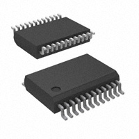
DB OR DW PACKAGE
(TOP VIEW)
Low Output Skew, Low Pulse Skew for
Clock-Distribution and Clock-Generation
Applications
Operates at 3.3-V VCC
LVTTL-Compatible Inputs and Outputs
Supports Mixed-Mode Signal Operation (5-V
Input and Output Voltages With 3.3-V VCC)
Distributes One Clock Input to Ten Outputs
Distributed VCC and Ground Pins Reduce
Switching Noise
High-Drive Outputs (–32-mA IOH, 32-mA IOL)
State-of-the-Art EPIC-IIB™ BiCMOS Design
Significantly Reduces Power Dissipation
Package Options Include Plastic
Small-Outline (DW) and Shrink Small-Outline
(DB) Packages
•
•
•
•
•
•
•
•
GND
Y10
VCC
Y9
OE
A
P0
P1
Y8
VCC
Y7
GND
1
24
2
3
23
22
4
5
21
20
6
7
19
18
8
9
17
16
10
15
11
12
14
13
GND
Y1
VCC
Y2
GND
Y3
Y4
GND
Y5
VCC
Y6
GND
DESCRIPTION
The CDC351 is a high-performance clock-driver circuit that distributes one input (A) to ten outputs (Y) with minimum
skew for clock distribution. The output-enable (OE) input disables the outputs to a high-impedance state. The
CDC351 operates at nominal 3.3-V VCC.
The propagation delays are adjusted at the factory using the P0 and P1 pins. The factory adjustments ensure that the
part-to-part skew is minimized and is kept within a specified window. Pins P0 and P1 are not intended for customer
use and should be connected to GND.
FUNCTION TABLE
INPUTS
A
OE
OUTPUTS
Yn
L
H
Z
H
H
Z
L
L
L
H
L
H
AVAILABLE OPTIONS
(1)
TA
Shrink Small-Outline Package (DB) (1)
Small-Outline Package (DW) (1)
0°C to 70°C
CDC351DB
CDC351DW
– 40°C to 85°C
CDC351IDB
CDC351IDW
This package is available tape and reel. Order by adding an R to the orderable part number (e.g., CDC351DBR).
EPIC-IIB is a trademark of Texas Instruments.
Please be aware that an important notice concerning availability, standard warranty, and use in critical applications of Texas Instruments
semiconductor products and disclaimers thereto appears at the end of this data sheet.
PRODUCTION DATA information is current as of publication date.
Products conform to specifications per the terms of Texas Instruments
standard warranty. Production processing does not necessarily include testing of all parameters.
Copyright © 1994 – 2003, Texas Instruments Incorporated
�CDC351. CDC351I
1-LINE TO 10-LINE CLOCK DRIVER WITH 3-STATE OUTPUTS
www.ti.com
SCAS441D – FEBRUARY 1994 – REVISED OCTOBER 2003
LOGIC SYMBOL
5
A
EN
OE
23
21
19
18
16
6
A
14
11
9
4
2
Y1
Y2
Y3
Y4
Y5
Y6
Y7
Y8
Y9
Y10
Note A: This symbol is in accordance with ANSI/IEEE Std 91-1984 and IEC Publication 617-12.
LOGIC DIAGRAM (POSITIVE LOGIC)
OE
5
23
21
19
18
A
Y2
Y3
Y4
6
16
7 8
P0 P1
14
11
9
4
2
2
Y1
Y5
Y6
Y7
Y8
Y9
Y10
�CDC351. CDC351I
1-LINE TO 10-LINE CLOCK DRIVER WITH 3-STATE OUTPUTS
www.ti.com
SCAS441D – FEBRUARY 1994 – REVISED OCTOBER 2003
ABSOLUTE MAXIMUM RATINGS
over operating free-air temperature range (unless otherwise noted) (1)
Supply voltage range, VCC
– 0.5 V to 4.6 V
Input voltage range, VI (2)
– 0.5 V to 7 V
VO (2)
Voltage range applied to any output in the
high state or power-off state,
– 0.5 V to 3.6 V
Current into any output in the low state, IO
64 mA
Input clamp current, IIK(VI < 0)
– 18 mA
Output clamp current, IOK (VI < 0)
Package thermal impedance ΘJA (3):
– 50 mA
DB package
147°C/ W
DW package
101°C/ W
Storage temperature range, Tstg
(1)
(2)
(3)
– 65°C to 150°C
Stresses beyond those listed under,, absolute maximum ratings” may cause permanent damage to the device. These are stress
ratings only, and functional operation of the device at these or any other conditions beyond those indicated under,, recommended
operating conditions” is not implied. Exposure to absolute-maximum-rated conditions for extended periods may affect device reliability.
The input and output negative-voltage ratings may be exceeded if the input and output clamp-current ratings are observed.
The package thermal impedance is calculated in accordance with JESD51.
RECOMMENDED OPERATING CONDITIONS (1)
MIN
MAX
3.6
VCC
Supply voltage
3
VIH
High-level input voltage
2
VIL
Low-level input voltage
VI
Input voltage
IOH
High-level output current
IOL
Low-level output current
fclock
Input clock frequency
TA
Operating free-air temperature
(1)
V
5.5
V
– 32
mA
32
mA
100
MHz
0
70
°C
– 40
85
°C
TYP
MAX
UNIT
–1.2
V
Commercial
Industrial
V
V
0.8
0
UNIT
Unused pins (input or I/O) must be held high or low.
ELECTRICAL CHARACTERISTICS
over recommended operating free-air temperature range (unless otherwise noted)
PARAMETER
TEST CONDITIONS
VIK
VCC = 3 V,
II = –18 mA
MIN
VOH
VCC = 3 V,
IOH = –32 mA
VOL
VCC = 3 V,
IOL = 32 mA
0.5
V
II
VCC = 3.6 V,
VI = VCC or GND
±1
µA
IO (1)
VCC = 3.6 V,
VO = 2.5 V
–150
mA
IOZ
VCC = 3.6 V,
VO = 3 V or 0
±10
µA
2
V
–15
Outputs high
0.3
Outputs low
25
ICC
VCC = 3.6 V, IO = 0, VI = VCC or GND
Ci
VI = VCC or GND,
VCC = 3.3 V,
f = 10 MHz
4
pF
Co
VO = VCC or GND,
VCC = 3.3 V,
f = 10 MHz
6
pF
Outputs disabled
(1)
mA
0.3
Not more than one output should be tested at a time, and the duration of the test should not exceed one second.
3
�CDC351. CDC351I
1-LINE TO 10-LINE CLOCK DRIVER WITH 3-STATE OUTPUTS
www.ti.com
SCAS441D – FEBRUARY 1994 – REVISED OCTOBER 2003
SWITICHING CHARACTERISTICS
CL = 50 pF (see Figure 1 and Figure 2)
FROM
(INPUT)
TO
(OUTPUT)
A
Y
OE
Y
OE
Y
tsk(o)
A
tsk(p)
A
tsk(pr)
A
Y
tr
A
tf
A
PARAMETER
tPLH
tPHL
tPZH
tPZL
tPHZ
tPLZ
VCC = 3.3 V, TA = 25°C
VCC = 3 V to 3.6 V,
TA = 0°C to 70°C
MIN
MAX
VCC = 3 V to 3.6 V,
TA = -40°C to 85°C
MIN
UNIT
MIN
TYP
MAX
MAX
3.2
3.7
4.2
3
3.5
4
1.8
3.8
5.5
1.3
5.9
1.1
6.1
1.8
3.8
5.5
1.3
5.9
1.1
6.1
1.8
3.9
5.9
1.7
6.3
1.5
6.5
1.8
4.2
5.9
1.7
6.4
1.5
6.6
Y
0.3
0.5
0.5
0.6
Y
0.2
0.8
0.8
0.9
ns
1
1
1.1
ns
Y
1.5
1.5
ns
Y
1.5
1.5
ns
ns
ns
ns
ns
SWITCHING CHARACTERISTICS TEMPERATURE AND VCC COEFFICIENTS
over recommended operating free-air temperature and VCC range (1)
PARAMETER
FROM
(INPUT)
TO
(OUTPUT)
MIN
MAX
UNIT
§tPLH(T)
Average temperature coefficient of low to high propagation
delay
A
Y
65 (2)
ps/10°C
§tPHL(T)
Average temperature coefficient of high to low propagation
delay
A
Y
45 (2)
ps/10°C
§tPLH(VCC)
Average VCC coefficient of low to high propagation delay
A
Y
§tPHL(VCC)
Average VCC coefficient of high to low propagation delay
A
Y
–140 (3)
–120 (3)
(1)
(2)
(3)
4
These data were extracted from characterization material and are not tested at the factory.
§tPLH(T) and §tPHL(T) are virtually independent of VCC.
§tPLH(VCC) and §tPHL(VCC) are virtually independent of temperature.
ps/ 100 mV
ps/ 100 mV
�CDC351. CDC351I
1-LINE TO 10-LINE CLOCK DRIVER WITH 3-STATE OUTPUTS
www.ti.com
SCAS441D – FEBRUARY 1994 – REVISED OCTOBER 2003
6V
500 Ω
From Output
Under Test
S1
TEST
tPLH /tPHL
tPLZ /tPZL
tPHZ /tPZH
Open
GND
CL = 50 pF
(see Note A)
S1
Open
6V
GND
500 Ω
tw
LOAD CIRCUIT
3V
Input
3V
Timing Input
1.5 V
1.5 V
0V
1.5 V
0V
tsu
VOLTAGE WAVEFORMS
th
3V
Data Input
1.5 V
1.5 V
0V
VOLTAGE WAVEFORMS
1.5 V
0V
tPHL
2V
0.8 V
tr
1.5 V
0V
tPLZ
1.5 V
tPLH
Output
1.5 V
tPZL
3V
Input
3V
Output
Control
(low-level
enabling)
1.5 V
VOH
2V
tf
0.8 V
VOL
3V
Output
Waveform 1
S1 at 6 V
(see Note B)
Output
Waveform 2
S1 at GND
(see Note B)
1.5 V
tPZH
VOLTAGE WAVEFORMS
VOL + 0.3 V
VOL
tPHZ
VOH
1.5 V
VOH - 0.3 V
≈0V
VOLTAGE WAVEFORMS
A. CL includes probe and jig capacitance.
B. Waveform 1 is for an output with internal conditions such that the output is low except when disabled by the output
control. Waveform 2 is for an output with internal conditions such that the output is high except when disabled by the
output control.
C. All input pulses are supplied by generators having the following characteristics: PRR ≤ 10 MHz, ZO = 50 Ω, tr≤ 2.5 ns,
tf≤ 2.5 ns.
D. The outputs are measured one at a time with one transition per measurement.
Figure 1. Load Circuit and Voltage Waveforms
5
�CDC351. CDC351I
1-LINE TO 10-LINE CLOCK DRIVER WITH 3-STATE OUTPUTS
SCAS441D – FEBRUARY 1994 – REVISED OCTOBER 2003
www.ti.com
A
Y1
tPHL1
tPLH1
tPHL2
tPLH2
tPHL3
tPLH3
tPHL4
tPLH4
tPHL5
tPLH5
tPHL6
tPLH6
tPHL7
tPLH7
tPHL8
tPLH8
tPHL9
tPLH9
Y2
Y3
Y4
Y5
Y6
Y7
Y8
Y9
Y10
tPHL10
tPLH10
A. Output skew, tsk(o), is calculated as the greater of:
— The difference between the fastest and slowest of tPLHn (n = 1, 2, 3, 4, 5, 6, 7, 8, 9, 10)
— The difference between the fastest and slowest of tPHLn(n = 1, 2, 3, 4, 5, 6, 7, 8, 9, 10)
B. Pulse skew, tsk(p), is calculated as the greater of | tPLHn - tPHLn | (n = 1, 2, 3, 4, 5, 6, 7, 8, 9, 10).
C. Process skew, tsk(pr), is calculated as the greater of:
— The difference between the fastest and slowest of tPLHn (n = 1, 2, 3, 4, 5, 6, 7, 8, 9, 10) across multiple devices under
identical operating conditions
— The difference between the fastest and slowest of tPHLn (n = 1, 2, 3, 4, 5, 6, 7, 8, 9, 10) across multiple devices under
identical operating conditions
Figure 2. Waveforms for Calculation of tsk(o), tsk(p), tsk(pr)
6
�PACKAGE OPTION ADDENDUM
www.ti.com
14-Oct-2022
PACKAGING INFORMATION
Orderable Device
Status
(1)
Package Type Package Pins Package
Drawing
Qty
Eco Plan
(2)
Lead finish/
Ball material
MSL Peak Temp
Op Temp (°C)
Device Marking
(3)
Samples
(4/5)
(6)
CDC351DB
ACTIVE
SSOP
DB
24
60
RoHS & Green
NIPDAU
Level-1-260C-UNLIM
0 to 70
CK351
Samples
CDC351DBR
ACTIVE
SSOP
DB
24
2000
RoHS & Green
NIPDAU
Level-1-260C-UNLIM
0 to 70
CK351
Samples
CDC351DW
ACTIVE
SOIC
DW
24
25
RoHS & Green
NIPDAU
Level-1-260C-UNLIM
0 to 70
CDC351
Samples
CDC351DWG4
ACTIVE
SOIC
DW
24
25
RoHS & Green
NIPDAU
Level-1-260C-UNLIM
0 to 70
CDC351
Samples
CDC351DWR
ACTIVE
SOIC
DW
24
2000
RoHS & Green
NIPDAU
Level-1-260C-UNLIM
0 to 70
CDC351
Samples
CDC351IDB
ACTIVE
SSOP
DB
24
60
RoHS & Green
NIPDAU
Level-1-260C-UNLIM
-40 to 85
CK351-I
Samples
CDC351IDBR
ACTIVE
SSOP
DB
24
2000
RoHS & Green
NIPDAU
Level-1-260C-UNLIM
-40 to 85
CK351-I
Samples
CDC351IDW
ACTIVE
SOIC
DW
24
25
RoHS & Green
NIPDAU
Level-1-260C-UNLIM
-40 to 85
CDC351-I
Samples
(1)
The marketing status values are defined as follows:
ACTIVE: Product device recommended for new designs.
LIFEBUY: TI has announced that the device will be discontinued, and a lifetime-buy period is in effect.
NRND: Not recommended for new designs. Device is in production to support existing customers, but TI does not recommend using this part in a new design.
PREVIEW: Device has been announced but is not in production. Samples may or may not be available.
OBSOLETE: TI has discontinued the production of the device.
(2)
RoHS: TI defines "RoHS" to mean semiconductor products that are compliant with the current EU RoHS requirements for all 10 RoHS substances, including the requirement that RoHS substance
do not exceed 0.1% by weight in homogeneous materials. Where designed to be soldered at high temperatures, "RoHS" products are suitable for use in specified lead-free processes. TI may
reference these types of products as "Pb-Free".
RoHS Exempt: TI defines "RoHS Exempt" to mean products that contain lead but are compliant with EU RoHS pursuant to a specific EU RoHS exemption.
Green: TI defines "Green" to mean the content of Chlorine (Cl) and Bromine (Br) based flame retardants meet JS709B low halogen requirements of


 工商网监
湘ICP备2023018690号
工商网监
湘ICP备2023018690号
