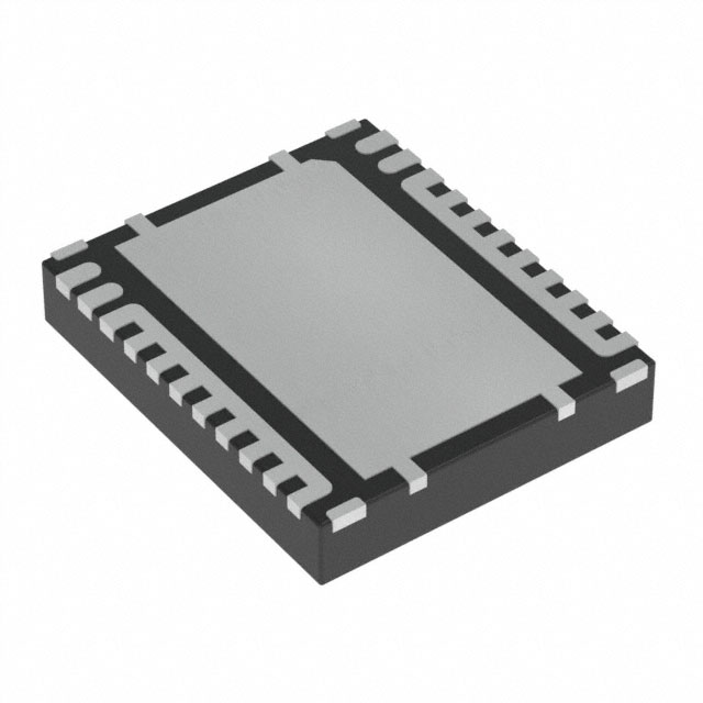
CSD88584Q5DC
SLPS598D – MAY 2017 – REVISED DECEMBER 2018
CSD88584Q5DC 40-V Half-Bridge NexFET™ Power Block
1 Features
3 Description
•
•
•
The CSD88584Q5DC 40-V power block is an
optimized design for high-current motor control
applications, such as handheld, cordless garden
and power tools. This device utilizes TI's patented
stacked die technology in order to minimize parasitic
inductances while offering a complete half bridge
in a space saving thermally enhanced DualCool™ 5mm × 6-mm package. With an exposed metal top,
this power block device allows for simple heat sink
application to draw heat out through the top of the
package and away from the PCB, for superior thermal
performance at the higher currents demanded by
many motor control applications.
2 Applications
•
•
•
Three-Phase Bridge for Brushless DC Motor
Control
Up to 8s Battery Power Tools
Other Half and Full Bridge Topologies
VIN
Bottom View
GL
NC
Top View
GH
SH
GH
VIN
VSW
SH
PGND
VSW
GL
PGND
Device Information
Copyright © 2017, Texas Instruments Incorporated
DEVICE
QTY
MEDIA
PACKAGE
SHIP
Power Block Schematic
CSD88584Q5DC
2500
13-Inch Reel
CSD88584Q5DCT
250
7-Inch Reel
SON
5.00-mm × 6.00-mm
Plastic Package
Tape
and
Reel
6
VIN
VM
GH_A
CSD88584
Motor
GL_A
DRV832X GH_B
Gate Driver GL_B
GH_C
CSD88584
Power Loss (W)
•
•
•
•
•
Half-bridge power block
High-density SON 5-mm × 6-mm footprint
Low RDS(ON) for minimized conduction losses
– 2.4-W PLoss at 35 A
DualCool™ thermally enhanced package
Ultra-Low-inductance package
RoHS compliant
Halogen free
Lead-free terminal plating
VIN = 24 V
VGS = 10 V
5 D.C. = 50%
L = 480 PH
fSW = 20 kHz
4 T = 25qC
A
3
2
CSD88584
1
GL_C
0
0
5
10
15
20
25
30
35
RMS Phase Current (A)
40
45
50
D000
Power Loss vs Output Current
Copyright © 2018, Texas Instruments Incorporated
Typical Circuit
An IMPORTANT NOTICE at the end of this data sheet addresses availability, warranty, changes, use in safety-critical applications,
intellectual property matters and other important disclaimers. PRODUCTION DATA.
�CSD88584Q5DC
www.ti.com
SLPS598D – MAY 2017 – REVISED DECEMBER 2018
Table of Contents
1 Features............................................................................1
2 Applications..................................................................... 1
3 Description.......................................................................1
4 Revision History.............................................................. 2
5 Specifications.................................................................. 3
5.1 Absolute Maximum Ratings(1) .................................... 3
5.2 Recommended Operating Conditions.........................3
5.3 Power Block Performance.......................................... 3
5.4 Thermal Information....................................................3
5.5 Electrical Characteristics.............................................4
5.6 Typical Power Block Device Characteristics............... 6
5.7 Typical Power Block MOSFET Characteristics........... 8
6 Application and Implementation.................................. 10
6.1 Application Information............................................. 10
6.2 Brushless DC Motor With Trapezoidal Control..........11
6.3 Power Loss Curves...................................................13
6.4 Safe Operating Area (SOA) Curve............................14
6.5 Normalized Power Loss Curves................................14
6.6 Design Example – Regulate Current to Maintain
Safe Operation............................................................ 14
6.7 Design Example – Regulate Board and Case
Temperature to Maintain Safe Operation.................... 14
7 Layout.............................................................................16
7.1 Layout Guidelines..................................................... 16
7.2 Layout Example........................................................ 18
8 Device and Documentation Support............................19
8.1 Receiving Notification of Documentation Updates....19
8.2 Support Resources................................................... 19
8.3 Trademarks............................................................... 19
8.4 Electrostatic Discharge Caution................................19
8.5 Glossary....................................................................19
9 Mechanical, Packaging, and Orderable Information.. 20
4 Revision History
Changes from Revision C (January 2018) to Revision D (December 2018)
Page
• Updated current sense resistor description in applications section ................................................................. 16
Changes from Revision * (May 2017) to Revision A (May 2017)
Page
• Updated Gate Driver part number in the Typical Circuit drawing........................................................................1
Changes from Revision A (May 2017) to Revision B (September 2017)
Page
• Updated Typical Safe Operating Area to extend to 50 A.................................................................................... 6
Changes from Revision B (September 2017) to Revision C (January 2018)
Page
• Changed VDD = 10 V to VGS = 10 V on the Power Loss vs Output Current Power Loss vs Output Current plot
............................................................................................................................................................................1
• Changed VDD to VGS in sections Recommended Operating Conditions, Block Performance, & Typical Power
Block Device Characteristics ............................................................................................................................. 3
• Changed IDSS test condition from 20 V to 32 V in the Electrical Characteristics table....................................... 4
2
Submit Document Feedback
Copyright © 2021 Texas Instruments Incorporated
Product Folder Links: CSD88584Q5DC
�CSD88584Q5DC
www.ti.com
SLPS598D – MAY 2017 – REVISED DECEMBER 2018
5 Specifications
5.1 Absolute Maximum Ratings(1)
TJ = 25°C (unless otherwise noted)
PARAMETER
Voltage
MIN
MAX
VIN to PGND
CONDITIONS
–0.8
40
VSW to PGND
–0.3
40
GH to SH
–20
20
GL to PGND
–20
V
20
Pulsed current rating, IDM (2)
Power dissipation, PD
Avalanche energy, EAS
UNIT
400
A
12
W
High-side FET, ID = 103 A, L = 0.1 mH
525
Low-side FET, ID = 103 A, L = 0.1 mH
525
mJ
Operating junction temperature, TJ
–55
150
°C
Storage temperature, Tstg
–55
150
°C
(1)
(2)
Stresses beyond those listed under Absolute Maximum Ratings may cause permanent damage to the device. These are stress ratings
only, and functional operation of the device at these or any other conditions beyond those indicated in the Recommended Operating
Conditions is not implied. Exposure to absolute-maximum-rated conditions for extended periods may affect device reliability.
Single FET conduction, max RθJC = 1.1°C/W, pulse duration ≤ 100 μs, single pulse.
5.2 Recommended Operating Conditions
TJ = 25°C (unless otherwise noted)
PARAMETER
VGS
MIN
MAX
4.5
16
voltage(1)
VIN
Input supply
ƒSW
Switching frequency
IOUT
RMS motor winding current
TJ
Operating temperature
(1)
CONDITIONS
Gate drive voltage
CBST = 0.1 µF (min)
5
UNIT
V
36
V
50
kHz
50
A
125
°C
Up to 32-V input use one capacitor per phase, MLCC 10 nF, 100 V, X7S, 0402, PN: C1005X7S2A103K050BB from VIN to GND return.
Between 32-V to 36-V input operation, add RC switch-node snubber as described in the Section 7.1.1 section of this data sheet.
5.3 Power Block Performance
TJ = 25°C (unless otherwise noted)
PARAMETER
PLOSS
PLOSS
(1)
CONDITIONS
MIN
TYP
MAX
UNIT
Power loss(1)
VIN = 24 V, VGS = 10 V,
IOUT = 35 A, ƒSW = 20 kHz,
TJ = 25°C, duty cycle = 50%,
L = 480 µH
2.4
W
Power loss
VIN = 24 V, VGS = 10 V,
IOUT = 35 A, ƒSW = 20 kHz,
TJ = 125°C, duty cycle = 50%,
L = 480 µH
3.5
W
Measurement made with eight 10-µF, 50-V, ±10% X5R (TDK C3225X5R1H106K250AB or equivalent) ceramic capacitors placed
across VIN to PGND pins and using UCC27210DDAR 100-V, 4-A driver IC.
5.4 Thermal Information
TJ = 25°C (unless otherwise stated)
THERMAL METRIC
RθJA
Junction-to-ambient thermal resistance (min Cu)(2)
Junction-to-ambient thermal resistance (max Cu)(2) (1)
MIN
TYP
MAX
125
50
UNIT
°C/W
Submit Document Feedback
Copyright © 2021 Texas Instruments Incorporated
Product Folder Links: CSD88584Q5DC
3
�CSD88584Q5DC
www.ti.com
SLPS598D – MAY 2017 – REVISED DECEMBER 2018
TJ = 25°C (unless otherwise stated)
THERMAL METRIC
RθJC
(1)
(2)
MIN
TYP
MAX
Junction-to-case thermal resistance (top of package)(2)
2.1
Junction-to-case thermal resistance (VIN pin)(2)
1.1
UNIT
°C/W
Device mounted on FR4 material with 1-in2 (6.45-cm2) Cu.
RθJC is determined with the device mounted on a 1-in2 (6.45-cm2), 2-oz (0.071-mm) thick Cu pad on a 1.5-in × 1.5-in
(3.81-cm × 3.81-cm), 0.06-in (1.52-mm) thick FR4 board. RθJC is specified by design while RθJA is determined by the user’s board
design.
5.5 Electrical Characteristics
TJ = 25°C (unless otherwise stated)
PARAMETER
TEST CONDITIONS
MIN
TYP
MAX
UNIT
STATIC CHARACTERISTICS
BVDSS
Drain-to-source voltage
VGS = 0 V, IDS = 250 µA
IDSS
Drain-to-source leakage current
VGS = 0 V, VDS = 32 V
IGSS
Gate-to-source leakage current
VDS = 0 V, VGS = 20 V
VGS(th)
Gate-to-source threshold voltage
VDS = VGS, IDS = 250 µA
RDS(on)
Drain-to-source on resistance
gfs
Transconductance
40
1.2
V
1.7
1
µA
100
nA
2.3
V
VGS = 4.5 V, IDS = 30 A
1.0
1.5
VGS = 10 V, IDS = 30 A
0.68
0.95
VDS = 4 V, IDS = 30 A
149
mΩ
S
DYNAMIC CHARACTERISTICS
CISS
Input capacitance
COSS
Output capacitance
9540
12400
pF
957
1240
pF
CRSS
RG
Reverse transfer capacitance
474
616
pF
Series gate resistance
1.0
2.0
Ω
Qg
Gate charge total (4.5 V)
Qg
Gate charge total (10 V)
68
88
nC
137
178
nC
Qgd
Gate charge gate-to-drain
Qgs
Gate charge gate-to-source
Qg(th)
Gate charge at Vth
QOSS
Output charge
td(on)
tr
td(off)
Turnoff delay time
tf
Fall time
VGS = 0 V, VDS = 20 V,
ƒ = 1 MHz
VDS = 20 V,
IDS = 30 A
26
nC
24
nC
16
nC
VDS = 20 V, VGS = 0 V
42
nC
Turnon delay time
11
ns
Rise time
VDS = 20 V, VGS = 10 V,
IDS = 30 A, RG = 0 Ω
24
ns
53
ns
17
ns
DIODE CHARACTERISTICS
4
VSD
Diode forward voltage
IDS = 30 A, VGS = 0 V
0.75
Qrr
Reverse recovery charge
nC
Reverse recovery time
VDS = 20 V, IF = 30 A,
di/dt = 300 A/µs
34
trr
24
ns
Submit Document Feedback
1.0
V
Copyright © 2021 Texas Instruments Incorporated
Product Folder Links: CSD88584Q5DC
�CSD88584Q5DC
www.ti.com
SLPS598D – MAY 2017 – REVISED DECEMBER 2018
Max RθJA = 50°C/W when mounted on 1 in2 (6.45 cm2) of
2-oz (0.071-mm) thick Cu.
Max RθJA = 125°C/W when mounted on minimum pad area
of 2-oz (0.071-mm) thick Cu.
Submit Document Feedback
Copyright © 2021 Texas Instruments Incorporated
Product Folder Links: CSD88584Q5DC
5
�CSD88584Q5DC
www.ti.com
SLPS598D – MAY 2017 – REVISED DECEMBER 2018
5.6 Typical Power Block Device Characteristics
The typical power block system characteristic curves (Power Loss vs Output Current through Normalized Power
Loss vs Duty Cycle) are based on measurements made on a PCB design with dimensions of 4 in (W) × 3.5 in (L)
× 0.062 in (H) and 6 copper layers of 2-oz copper thickness. See Section 6 section for detailed explanation. TJ =
125°C, unless stated otherwise.
10
1.2
Typical
Max
9
1.1
Power Loss, Normalized
Power Loss (W)
8
7
6
5
4
3
1
0.9
0.8
0.7
2
0.6
1
0
0
5
10
VIN = 24 V
ƒSW = 20 kHz
15
20
25
30
35
Output Current (A)
VGS = 10 V
L = 480 µH
40
45
50
-25
0
D001
VGS = 10 V
IOUT = 50 A
125
150
D002
D.C. = 50%
L = 480 µH
Figure 5-2. Power Loss vs Temperature
Figure 5-1. Power Loss vs Output Current
104
25
50
75
100
Junction Temperature (qC)
VIN = 24 V
ƒSW = 20 kHz
D.C. = 50%
100
55
0.5
-50
Top Case Temperature (qC)
108
112
116
120
124
128
TX
50
Output Current (A)
45
40
35
30
25
20
15
10
5
0
100
104
VIN = 24 V
ƒSW = 20 kHz
108
112
116
120
Board Temperature (qC)
VGS = 10 V
L = 480 µH
124
128
D005
D.C. = 50%
Figure 5-3. Typical Safe Operating Area
6
Submit Document Feedback
Copyright © 2021 Texas Instruments Incorporated
Product Folder Links: CSD88584Q5DC
�CSD88584Q5DC
www.ti.com
2.1
1.2
1.4
1.1
0.7
1
0.0
0.9
-0.7
0.8
5
10
15
VIN = 24 V
IOUT = 50 A
20
25
30
35
Switching Frequency (kHz)
VGS = 10 V
D. C. = 50%
40
45
-1.4
50
0.8
1.10
0.7
1.08
0.6
1.06
0.4
1.04
0.3
1.02
0.1
1.00
0.0
0.98
-0.1
0.96
-0.3
0.94
12
16
20
24
Input Voltage (V)
D006
L = 480 µH
IOUT = 50 A
ƒSW = 20 kHz
Figure 5-4. Normalized Power Loss vs Switching
Frequency
Power Loss, Normalized
1.12
VGS = 10 V
D. C. = 50%
0.8
1.10
0.7
1.08
0.6
1.06
0.4
1.04
0.3
1.02
0.1
1.00
0.0
20
VIN = 24 V
ƒSW = 20 kHz
30
40
50
60
70
Duty Cycle (%)
VGS = 10 V
L = 480 µH
-0.4
32
D007
L = 480 µH
Figure 5-5. Normalized Power Loss vs Input
Voltage
1.12
0.98
10
28
80
90
SOA Temperature Adj. (qC)
1.3
Power Loss, Normalized
2.8
SOA Temperature Adj. (qC)
Power Loss, Normalized
1.4
SOA Temperature Adj. (qC)
SLPS598D – MAY 2017 – REVISED DECEMBER 2018
-0.1
100
D009
IOUT = 50 A
Figure 5-6. Normalized Power Loss vs Duty Cycle
Submit Document Feedback
Copyright © 2021 Texas Instruments Incorporated
Product Folder Links: CSD88584Q5DC
7
�CSD88584Q5DC
www.ti.com
SLPS598D – MAY 2017 – REVISED DECEMBER 2018
5.7 Typical Power Block MOSFET Characteristics
450
200
400
180
IDS - Drain-to-Source Current (A)
Single Pulse Current (A)
TJ = 25°C, unless stated otherwise.
350
300
250
200
150
100
50
160
140
120
100
80
60
40
VGS = 4.5 V
VGS = 8 V
VGS = 10 V
20
0
1E-5
0
0.0001
0.001
0.01
Duration (s)
0.1
0
1
0.05
0.1
0.15
0.2
0.25
0.3
VDS - Drain-to-Source Voltage (V)
0.35
0.4
D010
Figure 5-8. MOSFET Saturation Characteristics
Max RθJA = 125°C/W
Figure 5-7. Single Pulse Current vs Pulse Duration
10
TC = 125° C
TC = 25° C
TC = -55° C
10
VGS - Gate-to-Source Voltage (V)
IDS - Drain-to-Source Current (A)
100
1
0.1
0.01
0.001
0
0.5
1
1.5
2
2.5
VGS - Gate-to-Source Voltage (V)
3
9
8
7
6
5
4
3
2
1
0
3.5
0
D012
15
VDS = 5 V
45
60
75
90 105
Qg - Gate Charge (nC)
ID = 30 A
Figure 5-9. MOSFET Transfer Characteristics
120
135
150
D014
VDS = 20 V
Figure 5-10. MOSFET Gate Charge
2.3
100000
Ciss = Cgd + Cgs
Coss = Cds + Cgd
Crss = Cgd
2.1
VGS(th) - Threshold Voltage (V)
C - Capacitance (pF)
30
10000
1000
1.9
1.7
1.5
1.3
1.1
0.9
0.7
100
0
10
20
30
VDS - Drain-to-Source Voltage (V)
40
D016
0.5
-75
-50
Figure 5-11. MOSFET Capacitance
-25
0
25
50
75 100 125
TC - Case Temperature (° C)
150
175
D018
ID = 250 µA
Figure 5-12. Threshold Voltage vs Temperature
8
Submit Document Feedback
Copyright © 2021 Texas Instruments Incorporated
Product Folder Links: CSD88584Q5DC
�CSD88584Q5DC
www.ti.com
SLPS598D – MAY 2017 – REVISED DECEMBER 2018
2
TC = 25° C
TC = 125° C
Normalized On-State Resistance
RDS(on) - On-State Resistance (m:)
5
4.5
4
3.5
3
2.5
2
1.5
1
0.5
2
4
6
8
10
12
14
16
VGS - Gate-to-Source Voltage (V)
18
1.6
1.4
1.2
1
0.8
0.6
0.4
-75
0
0
VGS = 4.5 V
VGS = 10 V
1.8
20
-25
0
25
50
75 100 125
TC - Case Temperature (° C)
ID = 30 A
ID = 30 A
150
175
D022
VDS = 20 V
Figure 5-14. MOSFET Normalized RDS(on) vs
Temperature
Figure 5-13. MOSFET RDS(on) vs VGS
100
1000
TC = 25° C
TC = 125° C
10
IAV - Peak Avalanche Current (A)
ISD - Source-to-Drain Current (A)
-50
D020
1
0.1
0.01
0.001
0.0001
0
0.2
0.4
0.6
0.8
VSD - Source-to-Drain Voltage (V)
1
TC = 25q C
TC = 125q C
100
10
1
0.01
D024
Figure 5-15. MOSFET Body Diode Forward Voltage
0.1
TAV - Time in Avalanche (ms)
1
D026
Figure 5-16. MOSFET Single Pulse Unclamped
Inductive Switching
Submit Document Feedback
Copyright © 2021 Texas Instruments Incorporated
Product Folder Links: CSD88584Q5DC
9
�CSD88584Q5DC
www.ti.com
SLPS598D – MAY 2017 – REVISED DECEMBER 2018
6 Application and Implementation
Note
Information in the following applications sections is not part of the TI component specification,
and TI does not warrant its accuracy or completeness. TI’s customers are responsible for
determining suitability of components for their purposes, as well as validating and testing their design
implementation to confirm system functionality.
6.1 Application Information
Historically, battery powered tools have favored brushed DC configurations to spin their primary motors, but
more recently, the advantages offered by brushless DC operation (BLDC) operation have brought about the
advent of popular designs that favor the latter. Those advantages include, but are not limited to higher efficiency
and therefore longer battery life, superior reliability, greater peak torque capability, and smooth operation over
a wider range of speeds. However, BLDC designs put increased demand for higher power density and current
handling capabilities on the power stage responsible for driving the motor.
The CSD88584Q5DC is part of TI’s power block product family and is a highly optimized product designed
explicitly for the purpose driving higher current DC motors in power and gardening tools. It incorporates TI’s
latest generation silicon which has been optimized for low resistance to minimize conduction losses and offer
excellent thermal performance. The power block utilizes TI’s stacked die technology to offer one complete half
bridge vertically integrated into a single 5-mm × 6-mm package with a DualCool exposed metal case. This
feature allows the designer to apply a heatsink to the top of the package and pull heat away from the PCB, thus
maximizing the power density while reducing the power stage footprint by up to 50%.
10
Submit Document Feedback
Copyright © 2021 Texas Instruments Incorporated
Product Folder Links: CSD88584Q5DC
�CSD88584Q5DC
www.ti.com
SLPS598D – MAY 2017 – REVISED DECEMBER 2018
6.2 Brushless DC Motor With Trapezoidal Control
The trapezoidal commutation control is simple and has fewer switching losses compared to sinusoidal control.
Vin
PB1
PWM1
DRV8323RX
SH1
TORQUE SET
MICROCONTROLLER
PWM2
SPEED SET
Vin
Q1
GH1
Vin
PB2
GH1
PB3
Q2
GH2
Vin
Q3
GH3
GL1
PWM3
PWM4
SH2
SH1
GH2
Three Phase
Gate Driver
SH3
Vsw1
SH2
Vsw3
Vsw2
GL2
PWM5
U
GH3
PWM6
Q4
GL1
SH3
VCS
Q5
GL2
N
Q6
A
B
C
GL3
PGND
SPA
A
B
C
Hall
Inputs
GL3
Hall
Sensors
SPA
PGND
SPB
PGND
SPC
V
S
W
SPB
SPC
0
Rcs1
0
Rcs2
0
Rcs3
0
Copyright © 2017, Texas Instruments Incorporated
Figure 6-1. Functional Block Diagram
The block diagram shown in Figure 6-1 offers a simple instruction of what is required to drive a BLDC motor:
one microcontroller, one three-phase driver IC, 3 power blocks (historically 6 power MOSFETs) and 3 Hall effect
sensors. The microcontroller responsible for block commutation must always know the rotor orientation or its
position relative to the stator coils. This is easy achieved with a brushed DC motor due to the fixed geometry and
position of the rotor windings, shaft and commutator.
A three-phase BLDC motor requires three Hall effect sensors or a rotary encoder to detect the rotor
position in relation to stator armature windings. Combining these three Hall effect sensors output signals, the
microcontroller can determine the proper commutation sequence. The three Hall sensors named A, B, and C
are mounted on the stator core at 120° intervals and the stator phase windings are implemented in a star
configuration. For every 60° of motor rotation, one Hall sensor changes its state. Based on the Hall sensor
outputs code, at the end of each block commutation interval the ampere conductors are commutated to the next
position. There are 6 steps needed to complete a full electrical cycle. The number of block commutation cycles
to complete a full mechanical rotation is determined by the number of rotor pole pairs.
Submit Document Feedback
Copyright © 2021 Texas Instruments Incorporated
Product Folder Links: CSD88584Q5DC
11
�CSD88584Q5DC
www.ti.com
SLPS598D – MAY 2017 – REVISED DECEMBER 2018
H a l l
c o d e
1 0 1
1 0 0
1 1 0
0 1 0
0 1 1
0 0 1
i _ U
0
i _ V
0
i _ W
0
Figure 6-2. Winding Current Waveforms on a BLDC Motor
Figure 6-2 above shows the three phase motor winding currents i_U, i_V, and i_W when running at 100% duty
cycle.
Trapezoidal commutation control offers the following advantages:
• Only two windings in series carry the phase winding current at any time while the third winding is open.
• Only one current sensor is necessary for all 3 windings U, V, and W.
• The position of the current sensor allows the use of low-cost shunt resistors.
However, trapezoidal commutation control has the disadvantage of commutation torque ripple. The current
sense on a three-phase inverter can be configured to use a single-shunt or three different sense resistors. For
cost sensitive applications targeting sensorless control, the three Hall effect sensors can be replaced with BEMF
voltage feedback dividers.
To obtain faster motor rotations and higher revolutions per minute (RPM), shorter periods and higher VIN voltage
are necessary. Contrarily, to reduce the rotational speed of the motor, it is necessary to lower the RMS voltage
applied across stator windings. This can easily be easily achieved by modulating the duty cycle, while maintain
a constant switching frequency. Frequency for the three-phase inverter chosen is usually low between 10 kHz to
50 kHz to reduce winding losses and to avoid audible noise.
12
Submit Document Feedback
Copyright © 2021 Texas Instruments Incorporated
Product Folder Links: CSD88584Q5DC
�CSD88584Q5DC
www.ti.com
SLPS598D – MAY 2017 – REVISED DECEMBER 2018
6.3 Power Loss Curves
CSD88584Q5DC was designed to operate up to 7-cell Li-Ion battery voltage applications ranging from 18 V to
32 V, typical 24 V. For 8s, input voltages between 32 V to 36 V, RC snubbers are required for each switch-node
U, V, and W. To reduce ringing, refer to the Section 7.1.1 section. In an effort to simplify the design process,
Texas Instruments has provided measured power loss performance curves over a variety of typical conditions.
Power Loss vs Output Current plots the CSD88584Q5DC power loss as a function of load current. The
measured power loss includes both input conversion loss and gate drive loss.
Equation 1 is used to generate the power loss curve:
Power loss (W) = (VIN × IIN_SHUNT) + (VDD × IDD_SHUNT) – (VSW_AVG × IOUT)
(1)
The power loss measurements were made on the circuit shown in Figure 6-3, power block devices for legs
U and V, PB1 and PB2 were disabled by shorting the CSD88584Q5DC high-side and low-side FETs gate-tosource terminals. Current shunt Iin_shunt provides Input current and Idd_SHUNT provides driver supply current
measurements. The winding current is measured from the DC load. An averaging circuit provides switch node W
equivalent RMS voltage.
Iin_SHUNT
PB1
Cin1
Vin
Vin
PB2
Cin2
PB3
Idd_SHUNT
Vin
Vdd
0
0
Vdd
GH2
GH1
SH2
SH1
Vsw1
Vin
GH3
0
0
U
Vsw2
SH3
HI
V
Vsw3
W
GATE
DRIVER
Lout
U 1A
1
GL2
GL1
PGND
0
0
2
LI
DCR
GL3
PGND
0
0
Iout
PGND
0
0
LOAD
0
0
AVERAGING
PWM
CIRCUIT
0
AVERAGE
SWITCH NODE
Vsw_AVG
Copyright © 2017, Texas Instruments Incorporated
Figure 6-3. Power Loss Test Circuit
The RMS current on the CSD88584Q5DC device depends on the motor winding current. For trapezoidal control,
the MOSFET RMS current is calculated using Equation 2.
IRMS = IOUT × √2
(2)
Taking into consideration system tolerances with the current measurement scheme, the inverter design needs to
withstand a 20% overload current.
Table 6-1. RMS and Overload Current Calculations
Winding RMS Current (A)
CSD88584Q5DC IRMS (A)
Overload 120% × IRMS (A)
30
42
51
40
56
68
50
70
85
Submit Document Feedback
Copyright © 2021 Texas Instruments Incorporated
Product Folder Links: CSD88584Q5DC
13
�CSD88584Q5DC
www.ti.com
SLPS598D – MAY 2017 – REVISED DECEMBER 2018
6.4 Safe Operating Area (SOA) Curve
The SOA curve in Typical Safe Operating Area provide guidance on the temperature boundaries within an
operating system by incorporating the thermal resistance and system power loss. This curve outlines the board
and case temperatures required for a given load current. The area under the curve dictates the safe operating
area. This curve is based on measurements made on a PCB design with dimensions of 4 in (W) × 3.5 in (L) ×
0.062 in (H) and 6 copper layers of 2-oz copper thickness.
6.5 Normalized Power Loss Curves
The normalized curves in the CSD88584Q5DC data sheet provide guidance on the power loss and SOA
adjustments based on application specific needs. These curves show how the power loss and SOA temperature
boundaries will adjust for different operation conditions. The primary Y-axis is the normalized change in power
loss while the secondary Y-axis is the change in system temperature required in order to comply with the SOA
curve. The change in power loss is a multiplier for the typical power loss. The change in SOA temperature is
subtracted from the SOA curve.
6.6 Design Example – Regulate Current to Maintain Safe Operation
If the case and board temperature of the power block are known, the SOA can be used to determine the
maximum allowed current that will maintain operation within the safe operating area of the device. The following
procedure outlines how to determine the RMS current limit while maintaining operation within the confines of the
SOA, assuming the temperatures of the top of the package and PCB directly underneath the part are known.
1. Start at the maximum current of the device on the Y-axis and draw a line from this point at the known top
case temperature to the known PCB temperature.
2. Observe where this point intersects the TX line.
3. At this intersection with the TX line, draw vertical line until you hit the SOA current limit. This intercept is the
maximum allowed current at the corresponding power block PCB and case temperatures.
In the example below, we show how to achieve this for the temperatures TC = 124°C and TB = 120°C. First we
draw from 50 A on the Y-axis at 124°C to 120°C on the X-axis. Then, we draw a line up from where this line
crosses the TX line to see that this line intercepts the SOA at 39 A. Thus we can assume if we are measuring
a PCB temperature of 124°C, and a top case temperature of 120°C, the power block can handle 39-A RMS, at
the normalized conditions. At conditions that differ from those in Power Loss vs Output Current, the user may be
required to make an SOA temperature adjustment on the TX line, as shown in the next section.
Figure 6-4. Regulating Current to Maintain Safe Operation
6.7 Design Example – Regulate Board and Case Temperature to Maintain Safe Operation
In the previous example we showed how given the PCB and case temperature, the current of the power block
could be limited to ensure operation within the SOA. Conversely, if the current and other application conditions
14
Submit Document Feedback
Copyright © 2021 Texas Instruments Incorporated
Product Folder Links: CSD88584Q5DC
�CSD88584Q5DC
www.ti.com
SLPS598D – MAY 2017 – REVISED DECEMBER 2018
are known, one can determine from the SOA what board or case temperature the user will need to limit their
design to. The user can estimate product loss and SOA boundaries by arithmetic means (see Section 6.7.1
section). Though the power loss and SOA curves in this data sheet are taken for a specific set of test conditions,
the following procedure outlines the steps the user should take to predict product performance for any set of
system conditions.
6.7.1 Operating Conditions
•
•
•
•
Winding output current (IOUT) = 40 A
Input voltage (VIN) = 32 V
Switching frequency (FSW) = 40 kHz
Duty cycle (D.C.) = 95%
6.7.2 Calculating Power Loss
•
•
•
•
•
Power loss at 40 A ≈ 4.7 W (Power Loss vs Output Current)
Normalized power loss for switching frequency ≈ 1.24 (Normalized Power Loss vs Switching Frequency)
Normalized power loss for input voltage ≈ 1.09 (Normalized Power Loss vs Input Voltage)
Normalized power loss for duty cycle ≈ 1.06 (Normalized Power Loss vs Duty Cycle)
Final calculated power loss = 4.7 W × 1.24 × 1.09 × 1.06 ≈ 6.7 W
6.7.3 Calculating SOA Adjustments
•
•
•
•
SOA adjustment for switching frequency ≈ 1.7°C (Normalized Power Loss vs Switching Frequency)
SOA adjustment for input voltage ≈ 0.6°C (Normalized Power Loss vs Input Voltage)
SOA adjustment for duty cycle ≈ 0.4°C (Normalized Power Loss vs Duty Cycle)
Final calculated SOA adjustment = 1.7 + 0.6 + 0.4 ≈ 2.7°C
In the Section 6.6 section above, the estimated power loss of the CSD88584Q5DC would increase to 6.7 W. In
addition, the maximum allowable board temperature would have to increase by 2.7°C. In Figure 6-5, the SOA
graph was adjusted accordingly.
1. Start by drawing a horizontal line from the application current (40 A) to the SOA curve.
2. Draw a vertical line from the SOA curve intercept down to the TX line.
3. Adjust the intersection point by subtracting the temperature adjustment value.
In this design example, the SOA board/ambient temperature adjustment yields a decrease of allowed junction
temperature of 2.7°C from 121.0°C to 118.3°C. Now it is known that the intersection of the case and PCB
temperatures on the TX line must stay below this point. For instance, if the power block case is observed
operating at 124°C, the PCB temperature must in turn be kept under 115°C to maintain this crossover point.
Figure 6-5. Regulate Temperature to Maintain Safe Operation
Submit Document Feedback
Copyright © 2021 Texas Instruments Incorporated
Product Folder Links: CSD88584Q5DC
15
�CSD88584Q5DC
www.ti.com
SLPS598D – MAY 2017 – REVISED DECEMBER 2018
7 Layout
The two key system-level parameters that can be optimized with proper PCB design are electrical and thermal
performance. A proper PCB layout will yield maximum performance in both areas. Below are some tips for how
to address each.
7.1 Layout Guidelines
7.1.1 Electrical Performance
The CSD88584Q5DC power block has the ability to switch at voltage rates greater than 1 kV/µs. Special care
must be then taken with the PCB layout design and placement of the input capacitors; high-current, high dI/dT
switching path; current shunt resistors; and GND return planes. As with any high-power inverter operated in
hard switching mode, there will be voltage ringing present on the switch nodes U, V, and W. Switch-node
ringing appears mainly at the HS FET turnon commutation with positive winding current direction. The U, V,
and W phase connections to the BLDC motor can be usually excluded from the ringing behavior since they
are subjected to high-peak currents but low dI/dT slew-rates. However, a compact PCB design with short and
low-parasitic loop inductances is critical to achieve low ringing and compliance with EMI specifications.
For safe and reliable operation of the three-phase inverter, motor phase currents have to be accurately
monitored and reported to the system microcontroller. One current sensor needs to be connected on each
motor phase winding U, V, and W. This sensing method is best for current sensing as it provides good accuracy
over a wide range of duty cycles, motor torque, and winding currents. Using current sensors is recommended
because it is less intrusive to the VIN and GND connections.
PB1
Vin
PB2
C4
GH1
PB3
Vin
C5
GH2
Vin
C6
GH3
0
0
0
SH3
SH2
SH1
U
Vsw
V
Vsw
W
Vsw
V in
C s1
GL3
GL2
GL1
C s3
C s2
PGND
PGND
PGND
R cs
R s1
R s2
R s3
GND
0
0
0
0
0
Copyright © 2017, Texas Instruments Incorporated
Figure 7-1. Recommended Ringing Reduction Components
However, for cost sensitive applications, current sensors are generally replaced with current sense resistors.
•
•
16
For designs using the 60-V three-phase smart gate driver DRV8320SRHBR, current sense resistor RCS can
be placed between common source terminals for all 3 power block devices CSD88584Q5DC to PGND and
measured using an external current sense amplifier as depicted in Figure 7-1 above.
For designs using the 60-V three-phase gate driver DRV8323RSRGZT, three current sense resistors RCS1,
RCS2 and RCS3 can be used between each CSD88584Q5DC source terminal to GND and measured by the
included DRV8323 current sense amplifiers. The three-phase driver IC should be placed as close as possible
to the power block gate GL and GH terminals.
Submit Document Feedback
Copyright © 2021 Texas Instruments Incorporated
Product Folder Links: CSD88584Q5DC
�CSD88584Q5DC
www.ti.com
SLPS598D – MAY 2017 – REVISED DECEMBER 2018
Breaking the high-current flow path from the source terminals of the power block to GND by introducing the RCS
current shunt resistors introduces parasitic PCB inductance. In the event the switch node waveforms exhibits
peak ringing that reaches undesirable levels, the ringing can be reduced by using the following ringing reduction
components:
•
•
•
The use of a high-side gate resistor in series with the GH pin is one effective way to reduce peak ringing.
The recommended HS FET gate resistor value will range between 4.7 Ω to 10 Ω depending on the driver IC
output characteristics used in conjunction with the power block device. The low-side FET gate pin GL should
connect directly to the driver IC output to avoid any parasitic cdV/dT turnon effect.
Low inductance MLCC caps C4, C5, and C6 can be used across each power block device from VIN
to the source terminal PGND. MLCC 10 nF, 100 V, ±10%, X7S, 0402, PN: C1005X7S2A103K050BB are
recommended.
Ringing can be reduced via the implementation of RC snubbers from each switch node U, V, and W to GND.
Recommended snubber component values are as follows:
– Snubber resistors Rs1, Rs2, Rs3: 2.21 Ω, 1%, 0.125 W, 0805, PN: CRCW08052R21FKEA
– Snubber caps Cs1, Cs2, and Cs3: MLCC 4.7 nF, 100 V, X7S, 0402, PN: C1005X7S2A472M050BB
With a switching frequency of 20 kHz on the three-phase inverter, the power dissipation on the RC snubber
resistor is 80 mW per channel. As a result, 0805 package size for resistors Rs1, Rs2, and Rs3 is adequate.
7.1.2 Thermal Considerations
The CSD88584Q5DC power block device has the ability to utilize the PCB copper planes as the primary thermal
path. As such, the use of thermal vias included in the footprint is an effective way to pull away heat from
the device and into the system board. Concerns regarding solder voids and manufacturability issues can be
addressed through the use of three basic tactics to minimize the amount of solder attach that will wick down the
via barrel:
• Intentionally space out the vias from one another to avoid a cluster of holes in a given area.
• Use the smallest drill size allowed by the design. The example in Figure 7-2 uses vias with a 10-mil drill hole
and a 16-mil solder pad.
• Tent the opposite side of the via with solder-mask. Ultimately the number and drill size of the thermal vias
should align with the end user’s PCB design rules and manufacturing capabilities.
To take advantage of the DualCool thermally enhanced package, an external heatsink can be applied on top of
the power block devices. For low EMI, the heatsink is usually connected to GND through the mounting screws
to the PCB. Gap pad insulators with good thermal conductivity should be used between the top of the package
and the heatsink. The Bergquist Sil-Pad 980 is recommended which provides excellent thermal impedance of
1.07°C/W at 50 psi.
Submit Document Feedback
Copyright © 2021 Texas Instruments Incorporated
Product Folder Links: CSD88584Q5DC
17
�CSD88584Q5DC
www.ti.com
SLPS598D – MAY 2017 – REVISED DECEMBER 2018
7.2 Layout Example
Figure 7-2. Top Layer
Figure 7-3. Bottom Layer
The placement of the input capacitors C4, C5, and C6 relative to VIN and PGND pins of CSD88584Q5DC device
should have the highest priority during the component placement routine. It is critical to minimize the VIN to GND
parasitic loop inductance. A shunt resistor R21 is used between all three U4, U5, and U6 power block source
terminals to the input supply GND return pin.
Input RMS current filtering is achieved via two bulk caps C17 and C18. Based on the RMS current ratings, the
recommended part number for input bulk is CAP AL, 330 µF, 63 V, ±20%, PN: EMVA630ADA331MKG5S.
18
Submit Document Feedback
Copyright © 2021 Texas Instruments Incorporated
Product Folder Links: CSD88584Q5DC
�CSD88584Q5DC
www.ti.com
SLPS598D – MAY 2017 – REVISED DECEMBER 2018
8 Device and Documentation Support
8.1 Receiving Notification of Documentation Updates
To receive notification of documentation updates, navigate to the device product folder on ti.com. Click on
Subscribe to updates to register and receive a weekly digest of any product information that has changed. For
change details, review the revision history included in any revised document.
8.2 Support Resources
TI E2E™ support forums are an engineer's go-to source for fast, verified answers and design help — straight
from the experts. Search existing answers or ask your own question to get the quick design help you need.
Linked content is provided "AS IS" by the respective contributors. They do not constitute TI specifications and do
not necessarily reflect TI's views; see TI's Terms of Use.
8.3 Trademarks
NexFET™, DualCool™, and are trademarks of TI.
TI E2E™ is a trademark of Texas Instruments.
All trademarks are the property of their respective owners.
8.4 Electrostatic Discharge Caution
This integrated circuit can be damaged by ESD. Texas Instruments recommends that all integrated circuits be handled
with appropriate precautions. Failure to observe proper handling and installation procedures can cause damage.
ESD damage can range from subtle performance degradation to complete device failure. Precision integrated circuits may
be more susceptible to damage because very small parametric changes could cause the device not to meet its published
specifications.
8.5 Glossary
TI Glossary
This glossary lists and explains terms, acronyms, and definitions.
Submit Document Feedback
Copyright © 2021 Texas Instruments Incorporated
Product Folder Links: CSD88584Q5DC
19
�CSD88584Q5DC
www.ti.com
SLPS598D – MAY 2017 – REVISED DECEMBER 2018
9 Mechanical, Packaging, and Orderable Information
The following pages include mechanical packaging and orderable information. This information is the most
current data available for the designated devices. This data is subject to change without notice and revision of
this document. For browser-based versions of this data sheet, refer to the left-hand navigation.
Table 9-1. Pin Configuration Table
20
POSITION
PIN NAME
DESCRIPTION
1
GH
High Side Gate
2
SH
High Side Gate Return
3-11
VSW
Switch Node
12-20
PGND
Power Ground
21
NC
No Connect
22
GL
Low Side Gate
23-26
NC
No Connect
27
VIN
Input Voltage
Submit Document Feedback
Copyright © 2021 Texas Instruments Incorporated
Product Folder Links: CSD88584Q5DC
�PACKAGE OUTLINE
DMM0022A
LSON-CLIP - 1.05 mm max height
SCALE 2.200
PLASTIC SMALL OUTLINE - NO LEAD
A
5.1
4.9
B
PIN 1 INDEX AREA
6.1
5.9
2X (0.35)
3.329 0.1
EXPOSED
HEAT SLUG
(0.701)
2.284 0.1
(1.486)
C
1.05 MAX
SEATING PLANE
0.05
0.00
0.08 C
3.3 0.1
4X (1.9)
4X
2X (2)
0.48
0.38
4X (0.25)
24
25
11
12
4X (0.175)
EXPOSED
THERMAL
PAD
(0.2) TYP
2X (0.3)
2X
5
PKG
27
5.4 0.1
1
20X 0.5
PIN 1 ID
(OPTIONAL)
23
26
SYMM
22X
22
0.55
0.45
22X
0.3
0.2
0.1
0.05
C A
C
B
4222731/B 07/2020
NOTES:
1. All linear dimensions are in millimeters. Any dimensions in parenthesis are for reference only. Dimensioning and tolerancing
per ASME Y14.5M.
2. This drawing is subject to change without notice.
3. The package thermal pad must be soldered to the printed circuit board for thermal and mechanical performance.
4. Tie bar size and position may vary.
www.ti.com
�EXAMPLE BOARD LAYOUT
DMM0022A
LSON-CLIP - 1.05 mm max height
PLASTIC SMALL OUTLINE - NO LEAD
(3.3)
22X (0.7)
4X (2.115)
26
23
(R0.05) TYP
1
22
22X (0.25)
21
2
3
20
20X (0.5)
4X
(3.013)
27
PKG
(5.4)
METAL UNDER
SOLDER MASK
2X
6X
(1.32)
SOLDER MASK
OPENING
2X
( 0.2) VIA
TYP
2X
(1.13)
11
(R0.05) TYP
12
24
6X (1.4)
25
SYMM
4X (0.375)
(0.3) TYP
4X (0.43)
(4.7)
LAND PATTERN EXAMPLE
SCALE:15X
0.05 MIN
ALL AROUND
0.05 MAX
ALL AROUND
SOLDER MASK
OPENING
METAL
METAL UNDER
SOLDER MASK
NON SOLDER MASK
DEFINED
PADS: 1, 2, 21-26
PAD 27: OPTIONAL
SOLDER MASK
OPENING
SOLDER MASK
DEFINED
PADS: 3-20
PAD 27: OPTIONAL
SOLDER MASK DETAILS
4222731/B 07/2020
NOTES: (continued)
5. This package is designed to be soldered to a thermal pad on the board. For more information, see Texas Instruments literature
number SLUA271 (www.ti.com/lit/slua271).
6. Vias are optional depending on application, refer to device data sheet. If some or all are implemented, recommended via locations are shown.
www.ti.com
�EXAMPLE STENCIL DESIGN
DMM0022A
LSON-CLIP - 1.05 mm max height
PLASTIC SMALL OUTLINE - NO LEAD
SYMM
22X (0.7)
4X (2.115)
METAL
TYP
23
26
8X (1.41)
27
1
22
22X (0.25)
2
21
3
8X
(1.12)
20
4X
(3.013)
20X (0.5)
SYMM
(0.66)
TYP
(R0.05) TYP
METAL UNDER
SOLDER MASK
2X
(1.32)
TYP
12
11
(0.8) TYP
24
4X (0.375)
25
(0.3) TYP
4X (0.43)
(4.7)
SOLDER PASTE EXAMPLE
BASED ON 0.125 mm THICK STENCIL
EXPOSED PAD 23
71% PRINTED SOLDER COVERAGE BY AREA UNDER PACKAGE
SCALE:20X
4222731/B 07/2020
NOTES: (continued)
7. Laser cutting apertures with trapezoidal walls and rounded corners may offer better paste release. IPC-7525 may have alternate
design recommendations.
www.ti.com
�PACKAGE OPTION ADDENDUM
www.ti.com
10-Dec-2020
PACKAGING INFORMATION
Orderable Device
Status
(1)
Package Type Package Pins Package
Drawing
Qty
Eco Plan
(2)
Lead finish/
Ball material
MSL Peak Temp
Op Temp (°C)
Device Marking
(3)
(4/5)
(6)
CSD88584Q5DC
ACTIVE
VSON-CLIP
DMM
22
2500
RoHS-Exempt
& Green
SN
Level-1-260C-UNLIM
-55 to 150
88584
CSD88584Q5DCT
ACTIVE
VSON-CLIP
DMM
22
250
RoHS-Exempt
& Green
SN
Level-1-260C-UNLIM
-55 to 150
88584
(1)
The marketing status values are defined as follows:
ACTIVE: Product device recommended for new designs.
LIFEBUY: TI has announced that the device will be discontinued, and a lifetime-buy period is in effect.
NRND: Not recommended for new designs. Device is in production to support existing customers, but TI does not recommend using this part in a new design.
PREVIEW: Device has been announced but is not in production. Samples may or may not be available.
OBSOLETE: TI has discontinued the production of the device.
(2)
RoHS: TI defines "RoHS" to mean semiconductor products that are compliant with the current EU RoHS requirements for all 10 RoHS substances, including the requirement that RoHS substance
do not exceed 0.1% by weight in homogeneous materials. Where designed to be soldered at high temperatures, "RoHS" products are suitable for use in specified lead-free processes. TI may
reference these types of products as "Pb-Free".
RoHS Exempt: TI defines "RoHS Exempt" to mean products that contain lead but are compliant with EU RoHS pursuant to a specific EU RoHS exemption.
Green: TI defines "Green" to mean the content of Chlorine (Cl) and Bromine (Br) based flame retardants meet JS709B low halogen requirements of


 工商网监
湘ICP备2023018690号
工商网监
湘ICP备2023018690号
