DAC161S055
www.ti.com
SNAS503B – NOVEMBER 2010 – REVISED JANUARY 2012
DAC161S055 Precision 16-Bit, Buffered Voltage-Output DAC
Check for Samples: DAC161S055
FEATURES
DESCRIPTION
•
•
•
•
The DAC161S055 is a precision 16-bit, buffered
voltage output Digital-to-Analog Converter (DAC) that
operates from a 2.7V to 5.25V supply with a separate
I/O supply pin that operates down to 1.7V. The onchip precision output buffer provides rail-to-rail output
swing and has a typical settling time of 5 µsec. The
external voltage reference can be set between 2.5V
and VA (the analog supply voltage), providing the
widest dynamic output range possible.
1
2
•
•
•
16-bit DAC with a Two-buffer SPI Interface
Asynchronous Load DAC and Reset Pins
Compatibility with 1.8V Controllers
Buffered Voltage Output with Rail-to-Rail
Capability
Wide Voltage Reference Range of +2.5V to VA
Wide Temperature Range of −40°C to +105°C
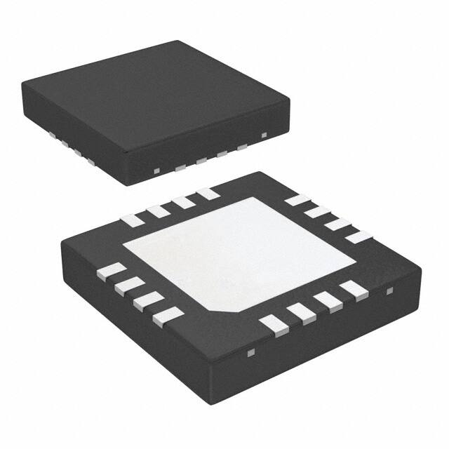
Packaged in a 16-pin WQFN
APPLICATIONS
•
•
•
•
•
•
•
Process Control
Automatic Test Equipment
Programmable Voltage Sources
Communication Systems
Data Acquisition
Industrial PLCs
Portable Battery Powered Instruments
KEY SPECIFICATIONS
•
•
•
•
•
•
Resolution (Specified Monotonic) 16 bits
INL ±3 LSB (max)
Very Low Output Noise 120 nV/√Hz (typ)
Glitch Impulse 7 nV-s (typ)
Output Settling Time 5 µs (typ)
Power Consumption 5.5 mW at 5.25 V (max)
The 4-wire SPI compatible interface operates at clock
rates up to 20 MHz. The part is capable of Diasy
Chain and Data Read Back. An on board power-onreset (POR) circuit ensures the output powers up to a
known state.
The DAC161S055 features a power-up value pin
(MZB), a load DAC pin (LDACB) and a DAC clear
(CLRB) pin. MZB sets the startup output voltage to
either GND or mid-scale. LDACB updates the output,
allowing multiple DACs to update their outputs
simultaneously. CLRB can be used to reset the
output signal to the value determined by MZB.
The DAC161S055 has a power-down option that
reduces power consumption when the part is not in
use. It is available in a 16-lead WQFN package.
1
2
Please be aware that an important notice concerning availability, standard warranty, and use in critical applications of
Texas Instruments semiconductor products and disclaimers thereto appears at the end of this data sheet.
All trademarks are the property of their respective owners.
PRODUCTION DATA information is current as of publication date.
Products conform to specifications per the terms of the Texas
Instruments standard warranty. Production processing does not
necessarily include testing of all parameters.
Copyright © 2010–2012, Texas Instruments Incorporated
�DAC161S055
SNAS503B – NOVEMBER 2010 – REVISED JANUARY 2012
www.ti.com
BLOCK DIAGRAM
VA Referenced Input
VA
MZB
VDDIO
VREF
CLRB
SDO
FIFO/
SPI/
INTERFACE
SDI
SCLK
16
CLR PRE
LOAD
16
PRE
REG
CLR PRE
LOAD
R-DAC
DAC
REG
Bypass
VOUT
BUF
CSB
10k
WRAL
WRUP
COMMANDS
GND
SWB
SEL_HIZ
LDACB
SEL_10K
VDDIO Referenced Inputs
CLR
COMMAND
VA
1
VOUT
2
VDDIO
MZB
CLRB
LDACB
16
15
14
13
CONNECTION DIAGRAM
12
CSB
11
SDI
WQFN 16
8
SDO
NC
9
7
4
GND
NC
6
SCLK
VREF
10
5
3
NC
NC
DAP
PIN DESCRIPTIONS
Pin #
WQFN-16
ESD Structure
Type
VDDIO
16
ESD
Clamp
Power
SPI, CLRB, LDACB Supply Voltage.
VA
1
ESD
Clamp
Power
Analog Supply Voltage.
Pin Name
2
Function and Connection
Submit Documentation Feedback
Copyright © 2010–2012, Texas Instruments Incorporated
Product Folder Links: DAC161S055
�DAC161S055
www.ti.com
SNAS503B – NOVEMBER 2010 – REVISED JANUARY 2012
PIN DESCRIPTIONS (continued)
Pin Name
Pin #
WQFN-16
ESD Structure
Type
Function and Connection
TO OUT DRIVE
VOUT
2
Analog Output
DAC output.
VREF
6
Analog Input
GND
7
Ground
SDI
11
Digital Input
SPI data input .
CSB
12
Digital Input
Chip select signal for SPI interface. On the falling edge of
CSB the chip begins to accept data and output data with
the SCLK signal. This pin is active low.
SCLK
10
Digital Input
Serial data clock for SPI Interface.
Voltage Reference Input.
Ground (Analog and Digital).
TO OUT DRIVE
SDO
9
Digital Output
Data Out for daisy chain or data read back verification.
LDACB
13
Digital Input
Load DAC signal. This signal transfers DAC data from
the SPI input register to the DAC output register. The
signal is active low.
CLRB
14
Digital Input
Asynchronous Reset. If this pin is pulled low, the output
will be updated to its power up condition set by the MZB
pin. This pin is active low.
MZB
15
Digital Input
Power up at Zero/Mid-scale. Tie this pin to GND to power
up to Zero or to VA to power up to mid-scale.
NC
DAP
3,4,5,8
DAP
No connect pins. Connect to GND in board layout will
result in the lowest amount of coupled noise.
Attach die attach paddle to GND for best noise
performance.
Submit Documentation Feedback
Copyright © 2010–2012, Texas Instruments Incorporated
Product Folder Links: DAC161S055
3
�DAC161S055
SNAS503B – NOVEMBER 2010 – REVISED JANUARY 2012
www.ti.com
These devices have limited built-in ESD protection. The leads should be shorted together or the device placed in conductive foam
during storage or handling to prevent electrostatic damage to the MOS gates.
ABSOLUTE MAXIMUM RATINGS
(1) (2)
−0.3V to 6.0V
Supply Voltage, VA
−0.3V to VA+0.3V
Supply Voltage VDDIO
6V, −0.3V
Any pin relative to GND
Voltage on MZB or VREF Input Pin
Voltage on any other Input Pin
(3)
−0.3V to VA+0.3V
(3)
−0.3V to VDDIO+0.3V
Voltage on VOUT (3)
Voltage on SDO
−0.3V to VA+0.3V
(3)
Input Current at Any Pin
−0.3V to VDDIO+0.3V
(3)
5mA
Output Current Source or Sink by Vout
10mA
Output Current Source or Sink by SDO
3mA
Total Package Input and Output Current
20mA
ESD Susceptibility
Human Body Model
Machine Model
Charged Device Model (CDM)
3000V
250V
1250V
−65°C to +150°C
Storage Temperature Range
Junction Temperature
+150°C
For soldering specifications: see product folder at www.ti.com and SNOA549
(1)
(2)
(3)
Absolute Maximum Ratings indicate limits beyond which damage to the device may occur, including inoperability and degradation of
device reliability and/or performance. Functional operation of the device and/or non-degradation at the Absolute Maximum Ratings or
other conditions beyond those indicated in the Recommended Operating Conditions is not implied. The recommended Operating
Conditions indicate conditions at which the device is functional and the device should not be operated beyond such conditions.
The Electrical characteristics tables list specifications under the listed Recommended Conditions except as otherwise modified or
specified by the Electrical Characteristics Conditions and/or Notes. Typical specifications are estimations only and are NOT specified.
When the input voltage (VI) at any pin exceeds the power supplies (VI < GND or VI > VDD) the current at that pin must be limited to
5mA and VI has to be within the Absolute Maximum Rating for that pin. The 20mA package input current rating limits the number of pins
that can safely exceed the power supplies with current flow to four.
RECOMMENDED OPERATING CONDITIONS
(1) (2)
−40°C to +105°C
Operating Temperature Range
Supply Voltage, VA
+2.7V to 5.25V
Supply Voltage VDDIO
+1.7 V to VA
Reference Voltage VREF
+2.5V to VA
Digital Input Voltage
0 to VDDIO
Output Load
0 to 200 pF
Package Thermal Resistance
θJA (3)
θJC
(1)
(2)
(3)
4
41°C/W
6.5°C/W
Absolute Maximum Ratings indicate limits beyond which damage to the device may occur, including inoperability and degradation of
device reliability and/or performance. Functional operation of the device and/or non-degradation at the Absolute Maximum Ratings or
other conditions beyond those indicated in the Recommended Operating Conditions is not implied. The recommended Operating
Conditions indicate conditions at which the device is functional and the device should not be operated beyond such conditions.
The Electrical characteristics tables list specifications under the listed Recommended Conditions except as otherwise modified or
specified by the Electrical Characteristics Conditions and/or Notes. Typical specifications are estimations only and are NOT specified.
The maximum power dissipation is a function of TJ(MAX) and θJA. The maximum allowable power dissipation at any ambient temperature
is PD=(TJ(MAX)-TA)/θJA
Submit Documentation Feedback
Copyright © 2010–2012, Texas Instruments Incorporated
Product Folder Links: DAC161S055
�DAC161S055
www.ti.com
SNAS503B – NOVEMBER 2010 – REVISED JANUARY 2012
ELECTRICAL CHARACTERISTICS
The following specifications apply for VA = 2.7V to 5.25V, VDDIO = VA, VREF = 2.5V to VA, RL = 10k to GND, CL = 200 pF to
GND, fSCLK = 20 MHz, input code range 512 to 65023. Boldface limits apply for TMIN ≤ TA ≤ TMAX: all other limits apply to TA
= 25°C, unless otherwise specified. (1) (2) (3)
Symbol
Parameter
Conditions
Min
Typ
Max
Units
STATIC PERFORMANCE
N
Resolution
16
INL
Integral Non-Linearity
No load. From code 512 to
Full Scale - 512. VA=5V, VREF=4.096V
DNL
Differential Non-Linearity
No load. From code 512 to
Full Scale - 512. VA=5V, VREF=4.096V
Bits
±1
-1
ZE
Zero Code Error
4
FSE
Full Scale Error
-15
OE
Offset Error
-11
Offset Error Drift
GE
Gain Error
Gain Temperature Coefficient
±1
±3
1.1
LSB
15
mV
15
mV
11
±4
No load. From code 512 to
Full Scale - 512. VA=5V, VREF=4.096V
No load. From code 512 to
Full Scale - 512. VA=5V, VREF=4.096V
mV
µV/°C
±0.05
-25
LSB
% of FS
25
±2
mV
ppm FS/°C
REFERENCE INPUT CHARACTERISTICS
VREF
Reference Input Voltage Range
VA = 2.7V to 5.25V
2.5
Reference Input Impedance
VA
12.5
V
kΩ
ANALOG OUTPUT CHARACTERISTICS
Output Voltage Range
No load.
DC Output Impedance
ZCO
FSO
CL
Zero Code Output
Full Scale Output
Maximum Capacitive Load
0.015
VA-0.04
V
Ω
2
VA=3V, IOUT=200 µA; VREF=2.5
3
VA=3V, IOUT=1mA; VREF=2.5
4
VA=5V, IOUT=200 µA; VREF=4.096
4
VA=5V, IOUT=1mA; VREF=4.096
4
VA=3V, IOUT=200 µA; VREF=2.5
2.495
VA=3V, IOUT=1mA; VREF=2.5
2.494
VA=5V, IOUT=200 µA; VREF=4.096
4.091
VA=5V, IOUT=1mA; VREF=4.096
4.089
mV
V
Parallel R = 10KΩ
500
pF
Series R = 50Ω
15
µF
RL
Minimum Resistive Load
10
kΩ
ISC
Short Circuit Current
VA = +5V, VREF=4.096
353
mA
tPU
Power-up Time
From Power Down Mode
25
ms
ANALOG OUTPUT DYNAMIC CHARCTERISTICS
SR
ts
(1)
(2)
(3)
Voltage Output Slew Rate
Positive and negative
2
V/µs
Voltage Output Settling Time
1/4 scale to 3/4 scale VREF= VA = +5V,
settle to ±1 LSB.
5
µs
Digital Feedthrough
Code 0, all digital inputs from GND to
VDDIO
1
nV-s
Major Code Transition Analog
Glitch Impulse
VA=5V, VREF=2.5V. Transition from midscale − 1LSB to mid-scale.
7
nV-s
Absolute Maximum Ratings indicate limits beyond which damage to the device may occur, including inoperability and degradation of
device reliability and/or performance. Functional operation of the device and/or non-degradation at the Absolute Maximum Ratings or
other conditions beyond those indicated in the Recommended Operating Conditions is not implied. The recommended Operating
Conditions indicate conditions at which the device is functional and the device should not be operated beyond such conditions.
The Electrical characteristics tables list specifications under the listed Recommended Conditions except as otherwise modified or
specified by the Electrical Characteristics Conditions and/or Notes. Typical specifications are estimations only and are NOT specified.
Typical values represent most likely parametric norms at specific conditions (Example VA; specific temperature) and at the
recommended Operating Conditions at the time of product characterizations and are NOT specified.
Submit Documentation Feedback
Copyright © 2010–2012, Texas Instruments Incorporated
Product Folder Links: DAC161S055
5
�DAC161S055
SNAS503B – NOVEMBER 2010 – REVISED JANUARY 2012
www.ti.com
ELECTRICAL CHARACTERISTICS (continued)
The following specifications apply for VA = 2.7V to 5.25V, VDDIO = VA, VREF = 2.5V to VA, RL = 10k to GND, CL = 200 pF to
GND, fSCLK = 20 MHz, input code range 512 to 65023. Boldface limits apply for TMIN ≤ TA ≤ TMAX: all other limits apply to TA
= 25°C, unless otherwise specified.(1) (2) (3)
Symbol
Parameter
Conditions
Min
Typ
Max
Units
Output Noise
Spot noise at 20 kHz
120
nV/√Hz
Integrated Output Noise
1Hz to 10 kHz
18
µV
DIGITAL INPUT CHARACTERISTICS
IIN
Input Current
VIL
Input Low Voltage
VIH
Input High Voltage
VILMZB
VIHMZB
CIN
MZB Input Low Voltage
MZB Input High Voltage
±1
VDDIO=5V
0.8
VDDIO=3V
0.8
VDDIO=1.8V
0.4
VDDIO=5V
2.1
VDDIO=3V
2.1
VDDIO=1.8V
1.4
µA
V
V
VA=5V
0.8
V
VA=3V
0.8
V
VA=5V
2.1
VA=3V
2.1
Input Capacitance
V
V
4
pF
DIGITAL OUTPUT CHARACTERISTICS
VOL
Output Low Voltage
Isink=200 µA; VDDIO>3V
400
Isink=2mA;VDDIO>3V
400
Isink=200 µA; VDDIO=1.8V
400
Isink=2mA;VDDIO=1.8V
VOH
Output High Voltage
lOZH, lOZL
COUT
400
Isink=200 µA; VDDIO>3V
VDDIO - 0.2
Isink=2mA;VDDIO>3V
VDDIO - 0.2
Isink=200 µA; VDDIO=1.8V
VDDIO - 0.2
Isink=2mA;VDDIO=1.8V
mV
V
1.15
TRI-STATE Leakage Current


 工商网监
湘ICP备2023018690号
工商网监
湘ICP备2023018690号
