Sample &
Buy
Product
Folder
Support &
Community
Tools &
Software
Technical
Documents
DRV8302
SLES267C – AUGUST 2011 – REVISED MARCH 2016
DRV8302 Three Phase Gate Driver With Dual Current Shunt Amplifiers and
Buck Regulator – Hardware Controlled
1 Features
3 Description
•
•
The DRV8302 is a gate driver IC for three phase
motor drive applications. It provides three half bridge
drivers, each capable of driving two N-channel
MOSFETs. The device supports up to 1.7-A source
and 2.3-A peak current capability. The DRV8302 can
operate off of a single power supply with a wide
range from 8-V to 60-V. It uses a bootstrap gate
driver architecture with trickle charge circuitry to
support 100% duty cycle. The DRV8302 uses
automatic hand shaking when the high side or low
side MOSFET is switching to prevent current shoot
through. Integrated VDS sensing of the high and low
side MOSFETs is used to protect the external power
stage against overcurrent conditions.
1
•
•
•
•
•
•
8-V to 60-V Operating Supply Voltage Range
1.7-A Source and 2.3-A Sink Gate Drive Current
Capability
Bootstrap Gate Driver With 100% Duty Cycle
Support
6 or 3 PWM Input Modes
Dual Integrated Current Shunt Amplifiers With
Adjustable Gain and Offset
3.3-V and 5-V Interface Support
Hardware Control Interface
Protection Features:
– Programmable Dead Time Control (DTC)
– Programmable Overcurrent Protection (OCP)
– PVDD and GVDD Undervoltage Lockout
(UVLO)
– GVDD Overvoltage Lockout (OVLO)
– Overtemperature Warning/Shutdown
(OTW/OTS)
– Reported through nFAULT and nOCTW pins
The DRV8302 also includes an integrated switching
mode buck converter with adjustable output and
switching frequency. The buck converter can provide
up to 1.5 A to support MCU or additional system
power needs.
A hardware interface allows for configuring various
device parameters including dead time, overcurrent,
PWM mode, and amplifier settings. Error conditions
are reported through the nFAULT and nOCTW pins.
2 Applications
•
•
•
•
•
•
The DRV8303 includes two current shunt amplifiers
for accurate current measurement. The amplifiers
support bi-directional current sensing and provide and
adjustable output offset up to 3 V.
3-Phase BLDC and PMSM Motors
CPAP and Pumps
E-Bikes
Power Tools
Robotics and RC Toys
Industrial Automation
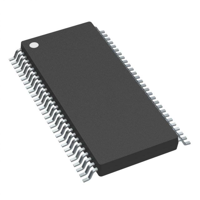
Device Information(1)
PART NUMBER
DRV8302
PACKAGE
BODY SIZE (NOM)
HTSSOP (56)
14.00 mm × 6.10 mm
(1) For all available packages, see the orderable addendum at
the end of the data sheet.
Simplified Schematic
8 to 60 V
HW Control
3-Phase
Brushless
Gate
Driver
MCU
Diff Amps
Sense
nFAULT
nOCTW
Gate Drive
MOSFETs
DRV8302
N-Channel
PWM
M
Buck
Converter
Vcc (Buck)
1
An IMPORTANT NOTICE at the end of this data sheet addresses availability, warranty, changes, use in safety-critical applications,
intellectual property matters and other important disclaimers. PRODUCTION DATA.
�DRV8302
SLES267C – AUGUST 2011 – REVISED MARCH 2016
www.ti.com
Table of Contents
1
2
3
4
5
6
Features ..................................................................
Applications ...........................................................
Description .............................................................
Revision History.....................................................
Pin Configuration and Functions .........................
Specifications.........................................................
6.1
6.2
6.3
6.4
6.5
6.6
6.7
6.8
6.9
7
1
1
1
2
3
5
Absolute Maximum Ratings ...................................... 5
ESD Ratings.............................................................. 5
Recommended Operating Conditions....................... 6
Thermal Information .................................................. 6
Electrical Characteristics........................................... 7
Gate Timing and Protection Characteristics ............. 8
Current Shunt Amplifier Characteristics.................... 8
Buck Converter Characteristics ................................ 9
Typical Characteristics ............................................ 10
Detailed Description ............................................ 11
7.1 Overview ................................................................. 11
7.2 Function Block Diagram.......................................... 12
7.3 Feature Description................................................. 13
7.4 Device Functional Modes........................................ 19
8
Application and Implementation ........................ 20
8.1 Application Information............................................ 20
8.2 Typical Application ................................................. 21
9
Power Supply Recommendations...................... 24
9.1 Bulk Capacitance .................................................... 24
10 Layout................................................................... 25
10.1 Layout Guidelines ................................................. 25
10.2 Layout Example .................................................... 25
11 Device and Documentation Support ................. 26
11.1
11.2
11.3
11.4
11.5
Documentation Support ........................................
Community Resources..........................................
Trademarks ...........................................................
Electrostatic Discharge Caution ............................
Glossary ................................................................
26
26
26
26
26
12 Mechanical, Packaging, and Orderable
Information ........................................................... 26
4 Revision History
NOTE: Page numbers for previous revisions may differ from page numbers in the current version.
Changes from Revision B (February 2016) to Revision C
Page
•
Deleted REG 0x02 from the test conditions of the Ioso1 and Iosi1 parameters in the Electrical Characteristics table ............ 7
•
Changed the value of R1 + R2 ≥ 100 KΩ to R1 + R2 ≥ 1 KΩ in the OC_ADJ section. ....................................................... 17
Changes from Revision A (December 2015) to Revision B
•
Page
Changed VEN_BUCK in Buck Converter Characteristics From: MIN = 0.9 V and MAX = 1.55 V To: MIN = 1.11 V
and MAX = 1.36 V. ................................................................................................................................................................ 9
Changes from Original (August 2011) to Revision A
Page
•
Added Pin Configuration and Functions section, ESD Rating table, Feature Description section, Device Functional
Modes, Application and Implementation section, Power Supply Recommendations section, Layout section, Device
and Documentation Support section, and Mechanical, Packaging, and Orderable Information section .............................. 1
•
VPVDD absolute max voltage rating reduced from 70 V to 65 V ............................................................................................. 5
•
Clarification made on how the OCP status bits report in Overcurrent Protection (OCP) and Reporting ............................ 16
•
Update to PVDD1 undervoltage protection in Undervoltage Protection (UVLO) describing specific transient brownout
issue. ................................................................................................................................................................................... 17
•
Update to EN_GATE pin functional description in EN_GATE clarifying proper EN_GATE reset pulse lengths. ................ 19
•
Added gate driver power-up sequencing errata Gate Driver Power Up Sequencing Errdata.............................................. 20
•
Added Community Resources ............................................................................................................................................. 24
2
Submit Documentation Feedback
Copyright © 2011–2016, Texas Instruments Incorporated
Product Folder Links: DRV8302
�DRV8302
www.ti.com
SLES267C – AUGUST 2011 – REVISED MARCH 2016
5 Pin Configuration and Functions
DCA Package
56-Pin HTSSOP With PowerPAD™
Top View
1
56
2
55
3
54
4
53
5
52
6
51
7
50
8
49
9
48
10
47
11
12
13
14
15
16
17
18
19
GND (57) - PowerPAD
RT_CLK
COMP
VSENSE
PWRGD
nOCTW
nFAULT
DTC
M_PWM
M_OC
GAIN
OC_ADJ
DC_CAL
GVDD
CP1
CP2
EN_GATE
INH_A
INL_A
INH_B
INL_B
INH_C
INL_C
DVDD
REF
SO1
SO2
AVDD
AGND
46
45
44
43
42
41
40
39
38
20
37
21
36
22
35
23
34
24
33
25
32
26
31
27
30
28
29
SS_TR
EN_BUCK
PVDD2
PVDD2
BST_BK
PH
PH
BIAS
BST_A
GH_A
SH_A
GL_A
SL_A
BST_B
GH_B
SH_B
GL_B
SL_B
BST_C
GH_C
SH_C
GL_C
SL_C
SN1
SP1
SN2
SP2
PVDD1
Pin Functions
PIN
NO.
NAME
I/O (1)
DESCRIPTION
RT_CLK
I
Resistor timing and external clock for buck regulator. Resistor should connect to GND (PowerPAD™)
with very short trace to reduce the potential clock jitter due to noise.
2
COMP
O
Buck error amplifier output and input to the output switch current comparator.
3
VSENSE
I
Buck output voltage sense pin. Inverting node of error amplifier.
4
PWRGD
I
An open drain output with external pullup resistor required. Asserts low if buck output voltage is low
due to thermal shutdown, dropout, overvoltage, or EN_BUCK shut down
5
nOCTW
O
Overcurrent and overtemperature warning indicator. This output is open drain with external pullup
resistor required.
6
nFAULT
O
Fault report indicator. This output is open drain with external pullup resistor required.
7
DTC
I
Dead-time adjustment with external resistor to GND
1
8
M_PWM
I
Mode selection pin for PWM input configuration. If M_PWM = LOW, the device supports 6 independent
PWM inputs. When M_PWM = HIGH, the device must be connected to ONLY 3 PWM input signals on
INH_x. The complementary PWM signals for low side signaling will be internally generated from the
high side inputs.
9
M_OC
I
Mode selection pin for over-current protection options. If M_OC = LOW, the gate driver will operate in a
cycle-by-cycle current limiting mode. If M_OC = HIGH, the gate driver will shutdown the channel which
detected an over-current event.
10
GAIN
O
Gain selection for integrated current shunt amplifiers. If GAIN = LOW, the internal current shunt
amplifiers have a gain of 10V/V. If GAIN = HIGH, the current shunt amplifiers have a gain of 40V/V.
11
OC_ADJ
I
Overcurrent trip set pin. Apply a voltage on this pin to set the trip point for the internal overcurrent
protection circuitry. A voltage divider from DVDD is recommended.
12
DC_CAL
I
When DC_CAL is high, device shorts inputs of shunt amplifiers and disconnects loads. DC offset
calibration can be done through external microcontroller.
(1)
KEY: I =Input, O = Output, P = Power
Submit Documentation Feedback
Copyright © 2011–2016, Texas Instruments Incorporated
Product Folder Links: DRV8302
3
�DRV8302
SLES267C – AUGUST 2011 – REVISED MARCH 2016
www.ti.com
Pin Functions (continued)
PIN
I/O (1)
DESCRIPTION
NO.
NAME
13
GVDD
P
Internal gate driver voltage regulator. GVDD cap should connect to GND
14
CP1
P
Charge pump pin 1, ceramic cap should be used between CP1 and CP2
15
CP2
P
Charge pump pin 2, ceramic cap should be used between CP1 and CP2
16
EN_GATE
I
Enable gate driver and current shunt amplifiers. Control buck via EN_BUCK pin.
17
INH_A
I
PWM Input signal (high side), half-bridge A
18
INL_A
I
PWM Input signal (low side), half-bridge A
19
INH_B
I
PWM Input signal (high side), half-bridge B
20
INL_B
I
PWM Input signal (low side), half-bridge B
21
INH_C
I
PWM Input signal (high side), half-bridge C
22
INL_C
I
PWM Input signal (low side), half-bridge C
23
DVDD
P
Internal 3.3-V supply voltage. DVDD cap should connect to AGND. This is an output, but not specified
to drive external circuitry.
24
REF
I
Reference voltage to set output of shunt amplfiiers with a bias voltage which equals to half of the
voltage set on this pin. Connect to ADC reference in microcontroller.
25
SO1
O
Output of current amplifier 1
26
SO2
O
Output of current amplifier 2
27
AVDD
P
Internal 6-V supply voltage, AVDD cap should connect to AGND. This is an output, but not specified to
drive external circuitry.
28
AGND
P
Analog ground pin
29
PVDD1
P
Power supply pin for gate driver and current shunt amplifier. PVDD1 is independent of buck power
supply, PVDD2. PVDD1 cap should connect to GND
30
SP2
I
Input of current amplifier 2 (connecting to positive input of amplifier). Recommend to connect to ground
side of the sense resistor for the best commom mode rejection.
31
SN2
I
Input of current amplifier 2 (connecting to negative input of amplifier).
32
SP1
I
Input of current amplifier 1 (connecting to positive input of amplifier). Recommend to connect to ground
side of the sense resistor for the best commom mode rejection.
33
SN1
I
Input of current amplifier 1 (connecting to negative input of amplifier).
34
SL_C
I
Low-Side MOSFET source connection, half-bridge C. Low-side VDS measured between this pin and
SH_C.
35
GL_C
O
Gate drive output for Low-Side MOSFET, half-bridge C
36
SH_C
I
High-Side MOSFET source connection, half-bridge C. High-side VDS measured between this pin and
PVDD1.
37
GH_C
O
Gate drive output for High-Side MOSFET, half-bridge C
38
BST_C
P
Bootstrap cap pin for half-bridge C
39
SL_B
I
Low-Side MOSFET source connection, half-bridge B. Low-side VDS measured between this pin and
SH_B.
40
GL_B
O
Gate drive output for Low-Side MOSFET, half-bridge B
41
SH_B
I
High-Side MOSFET source connection, half-bridge B. High-side VDS measured between this pin and
PVDD1.
42
GH_B
O
Gate drive output for High-Side MOSFET, half-bridge B
43
BST_B
P
Bootstrap cap pin for half-bridge B
44
SL_A
I
Low-Side MOSFET source connection, half-bridge A. Low-side VDS measured between this pin and
SH_A.
45
GL_A
O
Gate drive output for Low-Side MOSFET, half-bridge A
46
SH_A
I
High-Side MOSFET source connection, half-bridge A. High-side VDS measured between this pin and
PVDD1.
47
GH_A
O
Gate drive output for High-Side MOSFET, half-bridge A
48
BST_A
P
Bootstrap cap pin for half-bridge A
49
BIAS
I
Bias pin. Connect 1M-Ω resistor to GND, or 0.1 µF capacitor to GND.
PH
O
The source of the internal high side MOSFET of buck converter
50, 51
4
Submit Documentation Feedback
Copyright © 2011–2016, Texas Instruments Incorporated
Product Folder Links: DRV8302
�DRV8302
www.ti.com
SLES267C – AUGUST 2011 – REVISED MARCH 2016
Pin Functions (continued)
PIN
NO.
NAME
I/O (1)
DESCRIPTION
52
BST_BK
P
Bootstrap cap pin for buck converter
53, 54
PVDD2
P
Power supply pin for buck converter, PVDD2 cap should connect to GND.
55
EN_BUCK
I
Enable buck converter. Internal pullup current source. Pull below 1.2 V to disable. Float to enable.
Adjust the input undervoltage lockout with two resistors
56
SS_TR
I
Buck soft-start and tracking. An external capacitor connected to this pin sets the output rise time. Since
the voltage on this pin overrides the internal reference, it can be used for tracking and sequencing. Cap
should connect to GND
57
GND
(PWR_PAD)
P
GND pin. The exposed power pad must be electrically connected to ground plane through soldering to
PCB for proper operation and connected to bottom side of PCB through vias for better thermal
spreading.
6 Specifications
6.1 Absolute Maximum Ratings
over operating free-air temperature range (unless otherwise noted) (1)
MIN
MAX
–0.3
65
V
1
V/µs
VPVDD
Supply voltage
Relative to PGND
PVDDRAMP
Maximum supply voltage ramp rate
Voltage rising up to PVDDMAX
VPGND
Maximum voltage between PGND and GND
IIN_MAX
Maximum current, all digital and analog input pins except nFAULT and nOCTW pins
IIN_OD_MAX
Maximum sinking current for open-drain pins (nFAULT and nOCTW Pins)
VOPA_IN
Voltage range for SPx and SNx pins
VLOGIC
Input voltage range for logic/digital pins (INH_A, INL_A, INH_B, INL_B, INH_C, INL_C,
EN_GATE, M_PWM, M_OC, OC_ADJ, GAIN, DC_CAL)
VGVDD
Maximum voltage for GVDD pin
VAVDD
VDVDD
VREF
Maximum reference voltage for current amplifier
IREF
Maximum current for REF Pin
TJ
Maximum operating junction temperature
–40
Tstg
Storage temperature
–55
(1)
UNIT
–0.3
0.3
V
–1
1
mA
7
mA
–0.6
0.6
V
–0.3
7
V
13.2
V
Maximum voltage for AVDD pin
8
V
Maximum voltage for DVDD pin
3.6
V
7
V
100
µA
150
°C
150
°C
Stresses beyond those listed under Absolute Maximum Ratings may cause permanent damage to the device. These are stress ratings
only, which do not imply functional operation of the device at these or any other conditions beyond those indicated under Recommended
Operating Conditions. Exposure to absolute-maximum-rated conditions for extended periods may affect device reliability.
6.2 ESD Ratings
VALUE
V(ESD)
(1)
(2)
Electrostatic
discharge
Human-body model (HBM), per ANSI/ESDA/JEDEC JS-001 (1)
±2000
Charged-device model (CDM), per JEDEC specification JESD22-C101 (2)
±500
UNIT
V
JEDEC document JEP155 states that 500-V HBM allows safe manufacturing with a standard ESD control process.
JEDEC document JEP157 states that 250-V CDM allows safe manufacturing with a standard ESD control process.
Submit Documentation Feedback
Copyright © 2011–2016, Texas Instruments Incorporated
Product Folder Links: DRV8302
5
�DRV8302
SLES267C – AUGUST 2011 – REVISED MARCH 2016
www.ti.com
6.3 Recommended Operating Conditions
MIN NOM MAX
DC supply voltage PVDD1 for normal operation
VPVDD
Relative to PGND
DC supply voltage PVDD2 for buck converter
IDIN_EN
Input current of digital pins when EN_GATE is high
IDIN_DIS
Input current of digital pins when EN_GATE is low
CO_OPA
Maximum output capacitance on outputs of shunt amplifier
RDTC
Dead time control resistor range. Time range is 50 ns (–GND) to 500 ns (150 kΩ) with a
linear approximation.
IFAULT
FAULT pin sink current. Open drain
IOCTW
OCTW pin sink current. Open drain
VREF
External voltage reference voltage for current shunt amplifiers
fgate
Operating switching frequency of gate driver
TA
Ambient temperature
UNIT
8
60
3.5
60
V
V
100
µA
1
µA
20
pF
150
kΩ
V = 0.4 V
2
mA
V = 0.4 V
2
mA
6
V
0
2
Qg(TOT) = 25 nC or total 30-mA gate
drive average current
–40
200
kHz
125
°C
6.4 Thermal Information
DRV8302
THERMAL METRIC
(1)
DCA (HTSSOP)
UNIT
56 PINS
RθJA
Junction-to-ambient thermal resistance
30.3
°C/W
RθJC(top)
Junction-to-case (top) thermal resistance
33.5
°C/W
RθJB
Junction-to-board thermal resistance
17.5
°C/W
ψJT
Junction-to-top characterization parameter
0.9
°C/W
ψJB
Junction-to-board characterization parameter
7.2
°C/W
RθJC(bot)
Junction-to-case (bottom) thermal resistance
0.9
°C/W
(1)
6
For more information about traditional and new thermal metrics, see the Semiconductor and IC Package Thermal Metrics application
report (SPRA953).
Submit Documentation Feedback
Copyright © 2011–2016, Texas Instruments Incorporated
Product Folder Links: DRV8302
�DRV8302
www.ti.com
SLES267C – AUGUST 2011 – REVISED MARCH 2016
6.5 Electrical Characteristics
PVDD = 8 V to 60 V, TC = 25°C, unless specified under test condition
PARAMETER
TEST CONDITIONS
MIN
TYP MAX
UNIT
INPUT PINS: INH_X, INL_X, M_PWM, M_OC, GAIN, EN_GATE, DC_CAL
VIH
High input threshold
VIL
Low input threshold
2
REN_GATE
Internal pulldown resistor for EN_GATE
RINH_X
Internal pulldown resistor for high side PWMs
(INH_A, INH_B, and INH_C)
RINH_X
V
0.8
V
100
kΩ
EN_GATE high
100
kΩ
Internal pulldown resistor for low side PWMs
(INL_A, INL_B, and INL_C)
EN_GATE high
100
kΩ
RM_PWM
Internal pulldown resistor for M_PWM
EN_GATE high
100
kΩ
RM_OC
Internal pulldown resistor for M_OC
EN_GATE high
100
kΩ
RDC_CAL
Internal pulldown resistor for DC_CAL
EN_GATE high
100
kΩ
OUTPUT PINS: nFAULT AND nOCTW
VOL
Low output threshold
IO = 2 mA
VOH
High output threshold
External 47-kΩ pullup resistor connected to
3-5.5 V
0.4
IOH
Leakage current on open-drain pins When logic
high (nFAULT and nOCTW)
2.4
V
V
1
µA
11.5
V
GATE DRIVE OUTPUT: GH_A, GH_B, GH_C, GL_A, GL_B, GL_C
VGX_NORM
Gate driver Vgs voltage
PVDD = 8 V to 60 V
Ioso1
Maximum source current setting 1, peak
Vgs of FET equals to 2 V
9.5
1.7
A
Iosi1
Maximum sink current setting 1, peak
Vgs of FET equals to 8 V
2.3
A
Rgate_off
Gate output impedance during standby mode
when EN_GATE low (pins GH_x, GL_x)
1.6
2.4
kΩ
50
µA
SUPPLY CURRENTS
IPVDD1_STB
PVDD1 supply current, standby
EN_GATE is low. PVDD1 = 8 V.
20
IPVDD1_OP
PVDD1 supply current, operating
EN_GATE is high, no load on gate drive
output, switching at 10 kHz,
100-nC gate charge
15
IPVDD1_HIZ
PVDD1 Supply current, HiZ
EN_GATE is high, gate not switching
mA
2
5
11
mA
INTERNAL REGULATOR VOLTAGE
AVDD
AVDD voltage
6
6.5
7
V
DVDD
DVDD voltage
3
3.3
3.6
V
6
V
8
V
VOLTAGE PROTECTION
VPVDD_UV
Undervoltage protection limit, PVDD
VGVDD_UV
Undervoltage protection limit, GVDD
VGVDD_OV
Overvoltage protection limit, GVDD
16
V
CURRENT PROTECTION, (VDS SENSING)
VDS_OC
Drain-source voltage protection limit
Toc
OC sensing response time
0.125
1.5
2.4
µs
TOC_PULSE
OCTW pin reporting pulse stretch length for OC
event
64
µs
Submit Documentation Feedback
Copyright © 2011–2016, Texas Instruments Incorporated
Product Folder Links: DRV8302
V
7
�DRV8302
SLES267C – AUGUST 2011 – REVISED MARCH 2016
www.ti.com
6.6 Gate Timing and Protection Characteristics
MIN NOM
MAX
UNIT
TIMING, OUTPUT PINS
tpd,If-O
Positive input falling to GH_x falling
CL=1 nF, 50% to 50%
45
ns
tpd,Ir-O
Positive input rising to GL_x falling
CL=1 nF, 50% to 50%
45
ns
Td_min
Minimum dead time after hand
shaking (1)
Tdtp
Dead Time
With RDTC set to different values
tGDr
Rise time, gate drive output
CL=1 nF, 10% to 90%
25
ns
tGDF
Fall time, gate drive output
CL=1 nF, 90% to 10%
25
ns
TON_MIN
Minimum on pulse
Not including handshake communication.
Hiz to on state, output of gate driver
Tpd_match
Tdt_match
50
50
ns
500
ns
50
ns
Propagation delay matching between
high side and low side
5
ns
Deadtime matching
5
ns
10
ms
10
us
TIMING, PROTECTION AND CONTROL
tpd,R_GATE-OP
Start-up time, from EN_GATE active
high to device ready for normal
operation
PVDD is up before start-up, all charge
pump caps and regulator caps as in
recommended condition
tpd,R_GATE-Quick
If EN_GATE goes from high to low and
back to high state within quick reset
time, it will only reset all faults and gate
driver without powering down charge
pump, current amp, and related internal
voltage regulators.
Maximum low pulse time
tpd,E-L
Delay, error event to all gates low
200
ns
tpd,E-FAULT
Delay, error event to FAULT low
200
ns
OTW_CLR
Junction temperature for resetting
overtemperature warning
115
°C
130
°C
150
°C
5
Junction temperature for
OTW_SET/OTSD_C
overtemperature warning and resetting
LR
overtemperature shut down
OTSD_SET
(1)
Junction temperature for
overtemperature shut down
Dead time programming definition: Adjustable delay from GH_x falling edge to GL_X rising edge, and GL_X falling edge to GH_X rising
edge. This is a minimum dead-time insertion. It is not added to the value set by the microcontroller externally.
6.7 Current Shunt Amplifier Characteristics
TC = 25°C unless otherwise specified
MIN
TYP
MAX
UNIT
G1
Gain option 1
PARAMETER
(GAIN = 0 V)
9.5
10
10.5
V/V
G2
Gain option 2
(GAIN = 2 V)
38
40
42
V/V
Tsettling
Settling time to 1%
Tc = 0°C to 60°C, G = 10, Vstep = 2 V
Tsettling
Settling time to 1%
Tc = 0°C to 60°C, G = 40, Vstep = 2 V
Vswing
Output swing linear range
Slew Rate
TEST CONDITIONS
ns
1.2
0.3
G = 10
µs
5.7
10
DC_offset
Offset error RTI
Drift_offset
Offset drift RTI
Ibias
Input bias current
Vin_com
Common input mode range
Vin_dif
Differential input range
Vo_bias
Output bias
With zero input current, Vref up to 6 V
CMRR_OV
Overall CMRR with gain resistor
mismatch
CMRR at DC, gain = 10
8
300
G = 10 with input shorted
4
10
Submit Documentation Feedback
V
V/µs
mV
µV/C
100
µA
–0.15
0.15
V
–0.3
0.3
V
0.5%
V
–0.5%
0.5×Vref
70
85
dB
Copyright © 2011–2016, Texas Instruments Incorporated
Product Folder Links: DRV8302
�DRV8302
www.ti.com
SLES267C – AUGUST 2011 – REVISED MARCH 2016
6.8 Buck Converter Characteristics
TC = 25°C unless otherwise specified
PARAMETER
TEST CONDITIONS
MIN
TYP
VUVLO
Internal undervoltage lockout threshold
No voltage hysteresis, rising and falling
2.5
ISD(PVDD2)
Shutdown supply current
EN = 0 V, 25°C, 3.5 V ≤ VIN ≤ 60 V
1.3
INON_SW(PVDD2)
Operating: nonswitching supply current
VSENSE = 0.83 V, VIN = 12 V
VEN_BUCK
Enable threshold voltage
No voltage hysteresis, rising and falling
RDS_ON
On-resistance
VIN = 12 V, BOOT-PH = 6 V
ILIM
Current limit threshold
VIN = 12 V, TJ = 25°C
OTSD_BK
Thermal shutdown
Fsw
Switching frequency
PWRGD
1.11
1.8
RT = 200 kΩ
450
MAX
UNIT
V
4
µA
116
136
µA
1.25
1.36
V
200
410
mΩ
2.7
A
150
°C
581
720
kHz
VSENSE falling
92%
VSENSE rising
94%
VSENSE rising
109%
VSENSE falling
107%
Hysteresis
VSENSE falling
2%
Output high leakage
VSENSE = VREF, V(PWRGD) = 5.5 V,
25°C
10
nA
On resistance
I(PWRGD) = 3 mA, VSENSE < 0.79 V
50
Ω
VSENSE threshold
Submit Documentation Feedback
Copyright © 2011–2016, Texas Instruments Incorporated
Product Folder Links: DRV8302
9
�DRV8302
SLES267C – AUGUST 2011 – REVISED MARCH 2016
www.ti.com
10.0
12.0
9.8
11.8
9.6
11.6
9.4
11.4
GVDD (V)
IPVDD1 (µA)
6.9 Typical Characteristics
9.2
9.0
8.8
11.2
11.0
10.8
8.6
10.6
8.4
10.4
8.2
10.2
10.0
8.0
-40
0
25
85
-40
125
Temperature (ƒC)
0
25
85
Temperature (ƒC)
C001
125
C002
Figure 2. GVDD vs Temperature
(PVDD1 = 8 V, EN_GATE = HIGH)
Figure 1. IPVDD1 vs Temperature
(PVDD1 = 8 V, EN_GATE = LOW)
12.0
11.8
11.6
GVDD (V)
11.4
11.2
11.0
10.8
10.6
10.4
10.2
10.0
-40
0
25
85
Temperature (ƒC)
125
C001
Figure 3. GVDD vs Temperature (PVDD1 = 60 V, EN_GATE = HIGH)
10
Submit Documentation Feedback
Copyright © 2011–2016, Texas Instruments Incorporated
Product Folder Links: DRV8302
�DRV8302
www.ti.com
SLES267C – AUGUST 2011 – REVISED MARCH 2016
7 Detailed Description
7.1 Overview
The DRV8302 is a 8-V to 60-V, gate driver IC for three phase motor drive applications. This device reduces
external component count by integrating three half-bridge drivers, two current shunt amplifiers, and a switching
buck converter. The DRV8302 provides overcurrent, overtemperature, and undervoltage protection. Fault
conditions are indicated through the nFAULT and nOCTW pins.
Adjustable dead time control allows for finely tuning the switching of the external MOSFETs. Internal hand
shaking is used to prevent shoot-through current. VDS sensing of the external MOSFETs allows for the
DRV8302 to detect overcurrent conditions and respond appropriately. The VDS trip point can be set through a
hardware pin.
The highly configurable buck converter can support a wide range of output options. This allows the DRV8302 to
provide a power supply rail for the controller and lower voltage components.
Submit Documentation Feedback
Copyright © 2011–2016, Texas Instruments Incorporated
Product Folder Links: DRV8302
11
�DRV8302
SLES267C – AUGUST 2011 – REVISED MARCH 2016
www.ti.com
7.2 Function Block Diagram
PVDD2
DRV8302
PVDD2
EN_BUCK
VSENSE
PWRGD
VCC
BST_BK
Buck Converter
COMP
PH
SS_TR
RT_CLK
GVDD
GVDD
DVDD
DVDD
AVDD
Trickle Charge
DVDD
LDO
AVDD
LDO
Trickle
Charge
DVDD
CP1
AVDD
AGND
AVDD
Charge
Pump
Regulator
CP2
PVDD1
PVDD1
PVDD1
AGND
GVDD Trickle Charge
BST_A
PVDD1
AGND
nOCTW
HS VDS
Sense
HS
LS VDS
Sense
GVDD
GH_A
SH_A
nFAULT
M_PWM
Device
Configurations
and Fault
Reporting
M_OC
DVDD
LS
GL_A
SL_A
PVDD1
GAIN
GVDD Trickle Charge
BST_B
PVDD1
OC_ADJ
BIAS
HS VDS
Sense
HS
LS VDS
Sense
GVDD
GH_B
SH_B
EN_GATE
LS
INH_A
GL_B
SL_B
PVDD1
INL_A
GVDD Trickle Charge
BST_C
PVDD1
INH_B
Gate Driver
Control and
Timing Logic
INL_B
HS VDS
Sense
HS
LS VDS
Sense
GVDD
GH_C
SH_C
INH_C
INL_C
LS
DTC
GL_C
SL_C
REF
REF
SO1
SN1
Offset
½ REF
Current Sense
Amplifier 1
Offset
½ REF
Current Sense
Amplifier 2
SP1
RISENSE
REF
GND
DC_CAL
REF
SN2
SP2
RISENSE
SO2
GND
(PWR_PAD)
GND
PGND
AGND
12
GND
PGND
Submit Documentation Feedback
Copyright © 2011–2016, Texas Instruments Incorporated
Product Folder Links: DRV8302
�DRV8302
www.ti.com
SLES267C – AUGUST 2011 – REVISED MARCH 2016
7.3 Feature Description
7.3.1 Three-Phase Gate Driver
The half-bridge drivers use a bootstrap configuration with a trickle charge pump to support 100% duty cycle
operation. Each half-bridge is configured to drive two N-channel MOSFETs, one for the high-side and one for the
low-side. The half-bridge drivers can be used in combination to drive a 3-phase motor or separately to drive
various other loads.
The internal dead times are adjustable to accommodate a variety of external MOSFETs and applications. The
dead time is adjusted with an external resistor on the DTC pin. Shorting the DTC pin to ground provides the
minimum dead time (50 ns). There is an internal hand shake between the high side and low side MOSFETs
during switching transitions to prevent current shoot-through.
The three-phase gate driver can provide up to 30 mA of average gate driver current. This can support switching
frequencies up to 200 kHz when the MOSFET Qg = 25 nC. The high side gate drive will survive negative output
from the half-bridge up to –10 V for 10 ns. During EN_GATE low and fault conditions the gate driver keeps the
external MOSFETs in high impedance mode.
Each MOSFET gate driver has a VDS sensing circuit for overcurrent protection. The sense circuit measures the
voltage from the drain to the source of the external MOSFETs while the MOSFET is enabled. This voltage is
compared against the programmed trip point to determine if an overcurrent event has occurred. The trip voltage
is set through the OC_ADJ pin with a voltage usually set with a resistor divider. The high-side sense is between
the PVDD1 and SH_X pins. The low-side sense is between the SH_X and SL_X pins. Ensuring a differential, low
impedance connection to the external MOSFETs for these lines helps provide accurate VDS sensing. The
DRV8302 provides both cycle-by-cycle current limiting and latch overcurrent shutdown of the external MOSFET
through the M_OC pin.
The DRV8302 allows for both 6-PWM and 3-PWM control through the M_PWM pin.
Table 1. 6-PWM Mode
INL_X
INH_X
GL_X
GH_X
0
0
L
L
0
1
L
H
1
0
H
L
1
1
L
L
Table 2. 3-PWM Mode
INL_X
INH_X
GL_X
X
0
H
GH_X
L
X
1
L
H
Table 3. Gate Driver External Components
(1)
NAME
PIN 1
RnOCTW
nOCTW
VCC
PIN 2
(1)
≥10 kΩ
RnFAULT
nFAULT
VCC
(1)
≥10 kΩ
RDTC
DTC
GND (PowerPAD)
0 to 150 kΩ (50 ns to 500 ns)
CGVDD
GVDD
GND (PowerPAD)
2.2 µF (20%) ceramic, ≥ 16 V
CCP
CP1
CP2
CDVDD
DVDD
AGND
1 µF (20%) ceramic, ≥ 6.3 V
1 µF (20%) ceramic, ≥ 10 V
CAVDD
AVDD
AGND
CPVDD1
PVDD1
GND (PowerPAD)
CBST_X
BST_X
SH_X
RECOMMENDED
0.022 µF (20%) ceramic, rated for PVDD1
≥4.7 µF (20%) ceramic, rated for PVDD1
0.1 µF (20%) ceramic, ≥ 16 V
VCC is the logic supply to the MCU
Submit Documentation Feedback
Copyright © 2011–2016, Texas Instruments Incorporated
Product Folder Links: DRV8302
13
�DRV8302
SLES267C – AUGUST 2011 – REVISED MARCH 2016
www.ti.com
7.3.2 Current Shunt Amplifiers
The DRV8302 includes two high performance current shunt amplifiers to accurate low-side, inline current
measurement.
The current shunt amplifiers have 2 programmable GAIN settings through the GAIN pin. These are 10, and 40
V/V.
They provide output offset up to 3 V to support bidirectional current sensing. The offset is set to half the voltage
on the reference pin (REF).
To minimize DC offset and drift overtemperature, a calibration method is provided through either the DC_CAL
pin. When DC calibration is enabled, the device shorts the input of the current shunt amplifier and disconnect the
load. DC calibration can be done at any time, even during MOSFET switching, since the load is disconnected.
For the best results, perform the DC calibration during the switching OFF period, when no load is present, to
reduce the potential noise impact to the amplifier.
The output of current shunt amplifier can be calculated as:
V
VO = REF - G ´ (SNX - SPX )
2
where
•
•
•
VREF is the reference voltage (REF pin)
G is the gain of the amplifier (10 or 40 V/V)
SNX and SPx are the inputs of channel x
(1)
SPx should connect to resistor ground for the best common mode rejection.
Figure 4 shows current amplifier simplified block diagram.
DC_CAL
SN
200 kW
S2
50 kW
S1
5 kW
AVDD
_
100 W
DC_CAL
SO
5 kW
+
SP
50 kW
S1
200 kW
S2
DC_CAL
Vref /2
REF
_
AVDD
50 kW
+
50 kW
Figure 4. Current Shunt Amplifier Simplified Block Diagram
14
Submit Documentation Feedback
Copyright © 2011–2016, Texas Instruments Incorporated
Product Folder Links: DRV8302
�DRV8302
www.ti.com
SLES267C – AUGUST 2011 – REVISED MARCH 2016
7.3.3 Buck Converter
The DRV8302 uses an integrated TPS54160 1.5-A, 60-V, step-down DC-DC converter. Although integrated in
the same device, the buck converter is designed completely independent of the rest of the gate driver circuitry.
Because the buck converter can support external MCU or other external power need, the independency of buck
operation is crucial for a reliable system; this gives the buck converter minimum impact from gate driver
operations. Some examples are: when gate driver shuts down due to any failure, the buck still operates unless
the fault is coming from the buck itself. The buck keeps operating at much lower PVDD of 3.5 V, assuring the
system has a smooth power-up and power-down sequence when gate driver is not able to operate due to a low
PVDD.
For proper selection of the buck converter external components, see the data sheet, TPS54160 1.5-A, 60-V,
Step-Down DC/DC Converter With Eco-mode™, SLVSB56.
The buck has an integrated high-side N-channel MOSFET. To improve performance during line and load
transients the device implements a constant frequency, current mode control which reduces output capacitance
and simplifies external frequency compensation design.
The wide switching frequency of 300 kHz to 2200 kHz allows for efficiency and size optimization when selecting
the output filter components. The switching frequency is adjusted using a resistor to ground on the RT_CLK pin.
The device has an internal phase lock loop (PLL) on the RT_CLK pin that is used to synchronize the power
switch turn on to a falling edge of an external system clock.
The buck converter has a default start-up voltage of approximately 2.5 V. The EN_BUCK pin has an internal
pullup current source that can be used to adjust the input voltage undervoltage lockout (UVLO) threshold with
two external resistors. In addition, the pullup current provides a default condition. When the EN_BUCK pin is
floating the device will operate. The operating current is 116 µA when not switching and under no load. When the
device is disabled, the supply current is 1.3 µA.
The integrated 200-mΩ high-side MOSFET allows for high-efficiency power supply designs capable of delivering
1.5 A of continuous current to a load. The bias voltage for the integrated high side MOSFET is supplied by a
capacitor on the BOOT to PH pin. The boot capacitor voltage is monitored by an UVLO circuit that turns the high
side MOSFET off when the boot voltage falls below a preset threshold. The buck can operate at high duty cycles
because of the boot UVLO. The output voltage can be stepped down to as low as the 0.8-V reference.
The BUCK has a power good comparator (PWRGD) which asserts when the regulated output voltage is less
than 92% or greater than 109% of the nominal output voltage. The PWRGD pin is an open-drain output that
deasserts when the VSENSE pin voltage is between 94% and 107% of the nominal output voltage, allowing the
pin to transition high when a pullup resistor is used.
The BUCK minimizes excessive output overvoltage (OV) transients by taking advantage of the OV power good
comparator. When the OV comparator is activated, the high-side MOSFET is turned off and masked from turning
on until the output voltage is lower than 107%.
The SS_TR (slow start/tracking) pin is used to minimize inrush currents or provide power supply sequencing
during power-up. A small value capacitor should be coupled to the pin to adjust the slow start time. A resistor
divider can be coupled to the pin for critical power supply sequencing requirements. The SS_TR pin is
discharged before the output powers up. This discharging ensures a repeatable restart after an overtemperature
fault,
The BUCK, also, discharges the slow-start capacitor during overload conditions with an overload recovery circuit.
The overload recovery circuit slow-starts the output from the fault voltage to the nominal regulation voltage once
a fault condition is removed. A frequency foldback circuit reduces the switching frequency during start-up and
overcurrent fault conditions to help control the inductor current.
Submit Documentation Feedback
Copyright © 2011–2016, Texas Instruments Incorporated
Product Folder Links: DRV8302
15
�DRV8302
SLES267C – AUGUST 2011 – REVISED MARCH 2016
www.ti.com
Table 4. Buck Regulator External Components
(1)
NAME
PIN 1
PIN 2
RRT_CLK
RT_CLK
GND (PowerPAD)
See Buck Converter
RECOMMENDED
CCOMP
COMP
GND (PowerPAD)
See Buck Converter
RCCOMP
COMP
GND (PowerPAD)
See Buck Converter
RVSENSE1
PH (Filtered)
VSENSE
See Buck Converter
RVSENSE2
VSENSE
GND (PowerPAD)
See Buck Converter
VCC
(1)
≥ 10 kΩ
RPWRGD
PWRGD
LPH
PH
PH (Filtered)
See Buck Converter
DPH
PH
GND (PowerPAD)
See Buck Converter
CPH
PH (Filtered)
GND (PowerPAD)
See Buck Converter
CBST_BK
BST_BK
PH
See Buck Converter
CPVDD2
PVDD2
GND (PowerPAD)
≥4.7 µF (20%) ceramic, rated for PVDD2
CSS_TR
SS_TR
GND (PowerPAD)
See Buck Converter
VCC is the logic supply to the MCU
7.3.4 Protection Features
The DRV8302 provides a broad range of protection features and fault condition reporting. The DRV8302 has
undervoltage and overtemperature protection for the IC. It also has overcurrent and undervoltage protection for
the MOSFET power stage. In fault shut down conditions all gate driver outputs is held low to ensure the external
MOSFETs are in a high impedance state.
7.3.4.1 Overcurrent Protection (OCP) and Reporting
To protect the power stage from damage due to excessive currents, VDS sensing circuitry is implemented in the
DRV8302. Based on the RDS(on) of the external MOSFETs and the maximum allowed IDS, a voltage threshold can
be determined to trigger the overcurrent protection features when exceeded. The voltage threshold is
programmed through the OC_ADJ pin by applying an external reference voltage with a DAC or resistor divider
from DVDD. Overcurrent protection should be used as a protection scheme only; it is not intended as a precise
current regulation scheme. There can be up to a 20% tolerance across channels for the VDS trip point.
VDS = IDS ´ RDS(on)
(2)
The VDS sense circuit measures the voltage from the drain to the source of the external MOSFET while the
MOSFET is enabled. The high-side sense is between the PVDD and SH_X pins. The low-side sense is between
the SH_X and SL_X pins. Ensuring a differential, low impedance connection to the external MOSFETs for these
lines helps provide accurate VDS sensing.
There are two different overcurrent modes that can be set through the M_OC pin.
7.3.4.1.1 Current Limit Mode (M_OC = LOW)
In current limit mode the devices uses current limiting instead of device shutdown during an overcurrent event.
After the overcurrent event, the MOSFET in which the overcurrent was detected in will shut off until the next
PWM cycle. The overcurrent event will be reported through the nOCTW pin. The nOCTW pin will be held low for
a maximum 64 µs period (internal timer) or until the next PWM cycle. If another overcurrent event is triggered
from another MOSFET, during a previous overcurrent event, the reporting will continue for another 64 µs period
(internal timer will restart) or until both PWM signals cycle.
In current limit mode the device uses current limiting instead of device shutdown during an overcurrent event. In
this mode the device reports overcurrent events through the nOCTW pin. The nOCTW pin will be held low for a
maximum 64 µs period (internal timer) or until the next PWM cycle. If another overcurrent event is triggered from
another MOSFET, during a previous overcurrent event, the reporting will continue for another 64 µs period
(internal timer will restart) or until both PWM signals cycle.
16
Submit Documentation Feedback
Copyright © 2011–2016, Texas Instruments Incorporated
Product Folder Links: DRV8302
�DRV8302
www.ti.com
SLES267C – AUGUST 2011 – REVISED MARCH 2016
7.3.4.1.2 OC Latch Shutdown Mode
When an overcurrent event occurs, both the high-side and low-side MOSFETs will be disabled in the
corresponding half-bridge. The nFAULT pin will latch until the fault is reset through a quick EN_GATE reset
pulse.
7.3.4.2 OC_ADJ
When external MOSFET is turned on, the output current flows through the on resistance, RDS(on) of the MOSFET,
which creates a voltage drop VDS. The over current protection event will be enabled when the VDS exceeds a preset value. The voltage on OC_ADJ pin will be used to pre-set the OC tripped value. The OC tripped value IOC
has to meet following equations:
R2
´ DVDD = V DS
(R1 + R2)
where
•
•
IOC =
R1 + R2 ≥ 1 KΩ
DVDD = 3.3 V
(3)
VDS
RDS(on )
(4)
Connect OC_ADJ pin to DVDD to disable the over-current protection feature.
DVDD
R1
VOC
OC_ADJ
R2
Figure 5. OC_ADJ Current Programming Pin Connection
7.3.4.3 Undervoltage Protection (UVLO)
To protect the power output stage during start-up, shutdown, and other possible undervoltage conditions, the
DRV8302 provides undervoltage protection by driving the gate drive outputs (GH_X, GL_X) low whenever PVDD
or GVDD are below their undervoltage thresholds (PVDD_UV/GVDD_UV). This will put the external MOSFETs in
a high impedance state.
A specific PVDD1 undervoltage transient brownout from 13 to 15 µs can cause the DRV8302 to become
unresponsive to external inputs until a full power cycle. The transient condition consists of having PVDD1 greater
than the PVDD_UV level and then PVDD1 dropping below the PVDD_UV level for a specific period of 13 to 15
µs. Transients shorter or longer than 13 to 15 µs will not affect the normal operation of the undervoltage
protection. Additional bulk capacitance can be added to PVDD1 to reduce undervoltage transients.
7.3.4.4 Overvoltage Protection (GVDD_OV)
The device will shut down both the gate driver and charge pump if the GVDD voltage exceeds the GVDD_OV
threshold to prevent potential issues related to the GVDD pin or the charge pump (For example, short of external
GVDD cap or charge pump). The fault is a latched fault and can only be reset through a reset transition on the
EN_GATE pin.
Submit Documentation Feedback
Copyright © 2011–2016, Texas Instruments Incorporated
Product Folder Links: DRV8302
17
�DRV8302
SLES267C – AUGUST 2011 – REVISED MARCH 2016
www.ti.com
7.3.4.5 Overtemperature Protection
A two-level overtemperature detection circuit is implemented:
• Level 1: overtemperature warning (OTW)
OTW is reported through nOCTW pin.
• Level 2: overtemperature (OT) latched shut down of gate driver and charge pump (OTSD_GATE)
Fault will be reported to nFAULT pin. This is a latched shut down, so gate driver will not be recovered
automatically even if OT condition is not present anymore. An EN_GATE reset through pin is required to
recover gate driver to normal operation after temperature goes below a preset value, tOTSD_CLR.
7.3.4.6 Fault and Protection Handling
The nFAULT pin indicates an error event with shut down has occurred such as over-current, overtemperature,
overvoltage, or undervoltage. Note that nFAULT is an open-drain signal. nFAULT goes high when gate driver is
ready for PWM signal (internal EN_GATE goes high) during start-up.
The nOCTW pin indicates an overtemperature or over current event that is not necessarily related to shut down.
Following is the summary of all protection features and their reporting structure:
Table 5. Fault and Warning Reporting and Handling
EVENT
ACTION
LATCH
REPORTING ON
nFAULT PIN
REPORTING ON
nOCTW PIN
PVDD
undervoltage
External FETs HiZ;
Weak pulldown of all gate
driver output
N
Y
N
DVDD
undervoltage
External FETs HiZ;
Weak pulldown of all gate
driver output; When recovering,
reset all status registers
N
Y
N
GVDD
undervoltage
External FETs HiZ;
Weak pulldown of all gate
driver output
N
Y
N
GVDD
overvoltage
External FETs HiZ;
Weak pulldown of all gate driver output
Shut down the charge pump
Won’t recover and reset through
SPI reset command or
quick EN_GATE toggling
Y
Y
N
OTW
None
N
N
Y
OTSD_GATE
Gate driver latched shut down.
Weak pulldown of all gate driver output
to force external FETs HiZ
Shut down the charge pump
Y
Y
Y
OTSD_BUCK
OTSD of Buck
Y
N
N
Buck output
undervoltage
UVLO_BUCK: auto-restart
N
Y, in PWRGD pin
N
Buck overload
Buck current limiting
(HiZ high side until current reaches
zero and then auto-recovering)
N
N
N
External FET
overload – current limit
mode
External FETs current Limiting
(only OC detected FET)
N
N
Y
External FET
overload – Latch mode
Weak pulldown of gate driver
output and PWM logic “0” of
LS and HS in the same phase.
External FETs HiZ
Y
Y
Y
External FET
overload – reporting only
mode
Reporting only
N
N
Y
18
Submit Documentation Feedback
Copyright © 2011–2016, Texas Instruments Incorporated
Product Folder Links: DRV8302
�DRV8302
www.ti.com
SLES267C – AUGUST 2011 – REVISED MARCH 2016
7.4 Device Functional Modes
7.4.1 EN_GATE
EN_GATE low is used to put gate driver, charge pump, current shunt amplifier, and internal regulator blocks into
a low-power consumption mode to save energy. The device will put the MOSFET output stage to highimpedance mode as long as PVDD is still present.
When the EN_GATE pin goes low to high, it goes through a power-up sequence, and enable gate driver, current
amplifiers, charge pump, internal regulator, and so forth and reset all latched faults related to gate driver block.
All latched faults can be reset when EN_GATE is toggled after an error event unless the fault is still present.
When EN_GATE goes from high to low, it will shut down gate driver block immediately, so gate output can put
external FETs in high impedance mode. It will then wait for 10 µs before completely shutting down the rest of the
blocks. A quick fault reset mode can be done by toggling EN_GATE pin for a very short period (less than 10 µs).
This will prevent the device from shutting down the other functional blocks such as charge pump and internal
regulators and bring a quicker and simple fault recovery. To perform a full reset, EN_GATE should be toggled for
longer than 20 µs. This allows for all of the blocks to completely shut down and reach known states.
An EN_GATE reset pulse (high → low → high) from 10 to 20 µs should not be applied to the EN_GATE pin. The
DRV8301 has a transition area from the quick to full reset modes that can cause the device to become
unresponsive to external inputs until a full power cycle. An RC filter can be added externally to the pin if reset
pulses with this period are expected to occur on the EN_GATE pin.
One exception is to reset a GVDD_OV fault. A quick EN_GATE quick fault reset will not work with GVDD_OV
fault. A complete EN_GATE with low level holding longer than 20 µs is required to reset GVDD_OV fault. TI
highly recommends inspecting the system and board when GVDD_OV occurs.
7.4.2 DTC
Dead time can be programmed through DTC pin. A resistor should be connected from DTC to ground to control
the dead time. Dead time control range is from 50 ns to 500 ns. Short DTC pin to ground provides minimum
dead time (50 ns). Resistor range is 0 to 150 kΩ. Dead time is linearly set over this resistor range. Current shootthrough prevention protection will be enabled in the device all time independent of dead time setting and input
mode setting.
Submit Documentation Feedback
Copyright © 2011–2016, Texas Instruments Incorporated
Product Folder Links: DRV8302
19
�DRV8302
SLES267C – AUGUST 2011 – REVISED MARCH 2016
www.ti.com
8 Application and Implementation
NOTE
Information in the following applications sections is not part of the TI component
specification, and TI does not warrant its accuracy or completeness. TI’s customers are
responsible for determining suitability of components for their purposes. Customers should
validate and test their design implementation to confirm system functionality.
8.1 Application Information
The DRV8302 is a gate driver designed to drive a 3-phase BLDC motor in combination with external power
MOSFETs. The device provides a high level of integration with three half-bridge gate drivers, two current shunt
amplifiers, overcurrent protection, and a step-down buck regulator.
8.1.1 Gate Driver Power Up Sequencing Errdata
The DRV8301 gate drivers may not correctly power-up if a voltage greater than 8.5 V is present on any SH_X
pin when EN_GATE is brought logic high (device enabled) after PVDD1 power is applied (PVDD1 > PVDD_UV).
This sequence should be avoided by ensuring the voltage levels on the SH_X pins are less than 8.5 V when the
DRV8301 is enabled through EN_GATE.
20
Submit Documentation Feedback
Copyright © 2011–2016, Texas Instruments Incorporated
Product Folder Links: DRV8302
�DRV8302
www.ti.com
SLES267C – AUGUST 2011 – REVISED MARCH 2016
5
6
1
7
8
9
GPIO
10
11
DAC
12
2.2 µF
13
0.022 µF
14
15
16
17
18
19
PWM
20
21
22
1 µF
PVDDSENSE
23
24
ASENSE
ADC
BSENSE
25
56
26
1 µF
2200 pF
27
28
PVDD2
PWRGD
PVDD2
nOCTW
BST_BK
nFAULT
PH
DTC
PH
M_PWM
BIAS
M_OC
BST_A
GAIN
GH_A
OC_ADJ
SH_A
DC_CAL
GL_A
GVDD
SL_A
CP1
BST_B
CP2
GH_B
EN_GATE
SH_B
INH_A
GL_B
INL_A
SL_B
INH_B
BST_C
INL_B
GH_C
INH_C
SH_C
INL_C
GL_C
DVDD
SL_C
REF
SN1
SO1
SP1
SO2
SN2
AVDD
PPAD
2200 pF
CSENSE
56
EN_BUCK
VSENSE
AGND
SP2
PVDD1
55
X
54
53
52 0.1 µF
VCC
22 µH
51
50
+
1M
49
47 µF
4
GPIO
COMP
PVDD
56
4.7 µF
3
GPIO
0.015 µF
205 k
2
SS_TR
0.1 µF
POWE
R
RT_CLK
48 0.1 µF
47
GH_A
46
SH_A
45
GL_A
44
43 0.1 µF
42
SL_A
GH_B
41
SH_B
40
GL_B
39
38 0.1 µF
37
SL_B
GH_C
36
SH_C
35
GL_C
34
SL_C
33
SN1
32
SP1
31
SN2 PVDD
SP2
30
29
57
4.7 µF
10 k
DRV8302
1
10 k
10 k
10 k
MCU
VCC
0.1 µF
31.6 k
VCC
120 pF
6800 pF16.2 k
8.2 Typical Application
AGND GND PGND
PVDD
34.8 k
0.01 µF
3.3
PVDDSENSE
4.99 k
0.1 µF
10
Diff. Pair
SP2
AGND
GND
0.1 µF
BSENSE
SL_B
4.99 k
10
GL_B
CSENSE
34.8 k
4.99 k
SN2
VC
C
SH_B
10 m
ASENSE
4.99 k
10 m
SL_B
1000 pF
SP1
1000 pF
SL_A
10
GL_B
0.1 µF
10
GL_A
GH_B
VC
C
SH_B
34.8 k
SH_A
Diff. Pair
10
GH_B
VC
C
0.1 µF
GH_A
SN1
2.2 µF
2.2 µF
10
PVDD
PVDD
2.2 µF
PVDD
34.8 k
+
0.1 µF
+
220 µF
220 µF
VC
C
PGND
Figure 6. Typical Application Schematic
Submit Documentation Feedback
Copyright © 2011–2016, Texas Instruments Incorporated
Product Folder Links: DRV8302
21
�DRV8302
SLES267C – AUGUST 2011 – REVISED MARCH 2016
www.ti.com
Typical Application (continued)
Example:
Buck: PVDD = 3.5 V – 40 V, Iout_max = 1.5 A, Vo = 3.3 V, Fs = 570 kHz
8.2.1 Design Requirements
Table 6. Design Parameters
DESIGN PARAMETER
REFERENCE
Supply voltage
VALUE
PVDD
24 V
MR
0.5 Ω
Motor winding inductance
ML
0.28 mH
Motor poles
MP
16 poles
MRPM
4000 RPM
Motor winding resistance
Motor rated RPM
Target full-scale current
Sense resistor
MOSFET Qg
14 A
0.01 Ω
Qg
29 nC
RDS(on)
4.7 mΩ
OC_ADJ_SET
0.123 V
ƒSW
45 kHz
RGATE
10 Ω
MOSFET RDS(on)
VDS trip level
IMAX
RSENSE
Switching frequency
Series gate resistance
Amplifier reference
VREF
3.3 V
Amplifier gain
Gain
10 V/V
8.2.2 Detailed Design Procedure
8.2.2.1 Gate Drive Average Current Load
The gate drive supply (GVDD) of the DRV8302 can deliver up to 30 mA (RMS) of current to the external power
MOSFETs. Use Equation 5 to determine the approximate RMS load on the gate drive supply:
Gate Drive RMS Current = MOSFET Qg × Number of Switching MOSFETs × Switching Frequency
(5)
Example:
7.83 mA = 29 nC × 6 × 45 kHz
(6)
This is a rough approximation only.
8.2.2.2 Overcurrent Protection Setup
The DRV8302 provides overcurrent protection for the external power MOSFETs through the use of VDS
monitors for both the high side and low side MOSFETs. These are intended for protecting the MOSFET in
overcurrent conditions and not for precise current regulation.
The overcurrent protection works by monitoring the VDS voltage of the external MOSFET and comparing it
against the OC_ADJ pin voltage. If the VDS exceeds the OC_ADJ pin voltage the DRV8302 takes action
according to the M_OC pin.
Overcurrent Trip = OC_ADJ_SET / MOSFET RDS(on)
(7)
Example:
26.17 A = 0.123 V/ 4.7 mΩ
(8)
MOSFET RDS(on) changes with temperature and this will affect the overcurrent trip level.
8.2.2.3 Sense Amplifier Setup
The DRV8302 provides two bidirectional low-side current shunt amplifiers. These can be used to sense a sum of
the three half-bridges, two of the half-bridges individually, or in conjunction with an additional shunt amplifier to
sense all three half-bridges individually.
1. Determine the peak current that the motor will demand (IMAX). This will be dependent on the motor
22
Submit Documentation Feedback
Copyright © 2011–2016, Texas Instruments Incorporated
Product Folder Links: DRV8302
�DRV8302
www.ti.com
SLES267C – AUGUST 2011 – REVISED MARCH 2016
parameters and your specific application. I(MAX) in this example is 14 A.
2. Determine the available voltage range for the current shunt amplifier. This will be ± half of the amplifier
reference voltage (VREF). In this case the available range is ±1.65 V.
3. Determine the sense resistor value and amplifier gain settings. There are common tradeoffs for both the
sense resistor value and amplifier gain. The larger the sense resistor value, the better the resolution of the
half-bridge current. This comes at the cost of additional power dissipated from the sense resistor. A larger
gain value will allow you to decrease the sense resistor, but at the cost of increased noise in the output
signal. This example uses a 0.01-Ω sense resistor and the minimum gain setting of the DRV8302 (10 V/V).
These values allow the current shunt amplifiers to measure ±16.5 A (some additional margin on the 14-A
requirement).
8.2.3 Application Curves
Figure 7. Motor Spinning 2000 RPM
Figure 8. Motor Spinning 4000 RPM
Figure 9. Gate Drive 20% Duty Cycle
Figure 10. Gate Drive 80% Duty Cycle
Submit Documentation Feedback
Copyright © 2011–2016, Texas Instruments Incorporated
Product Folder Links: DRV8302
23
�DRV8302
SLES267C – AUGUST 2011 – REVISED MARCH 2016
www.ti.com
9 Power Supply Recommendations
9.1 Bulk Capacitance
Having appropriate local bulk capacitance is an important factor in motor drive system design. It is generally
beneficial to have more bulk capacitance, while the disadvantages are increased cost and physical size.
The amount of local capacitance needed depends on a variety of factors, including:
• The highest current required by the motor system
• The capacitance of the power supply and its ability to source or sink current
• The amount of parasitic inductance between the power supply and motor system
• The acceptable voltage ripple
• The type of motor used (brushed DC, brushless DC, stepper)
• The motor braking method
The inductance between the power supply and motor drive system will limit the rate current can change from the
power supply. If the local bulk capacitance is too small, the system will respond to excessive current demands or
dumps from the motor with a change in voltage. When adequate bulk capacitance is used, the motor voltage
remains stable and high current can be quickly supplied.
The data sheet generally provides a recommended value, but system-level testing is required to determine the
appropriate sized bulk capacitor.
Power Supply
Parasitic Wire
Inductance
Motor Drive System
VM
+
–
+
Motor
Driver
GND
Local
Bulk Capacitor
IC Bypass
Capacitor
Figure 11. Example Setup of Motor Drive System With External Power Supply
The voltage rating for bulk capacitors should be higher than the operating voltage, to provide margin for cases
when the motor transfers energy to the supply.
24
Submit Documentation Feedback
Copyright © 2011–2016, Texas Instruments Incorporated
Product Folder Links: DRV8302
�DRV8302
www.ti.com
SLES267C – AUGUST 2011 – REVISED MARCH 2016
10 Layout
10.1 Layout Guidelines
Use these layout recommendations when designing a PCB for the DRV8302.
• The DRV8302 makes an electrical connection to GND through the PowerPAD. Always check to ensure that
the PowerPAD has been properly soldered (See the application report, PowerPAD™ Thermally Enhanced
Package application report, SLMA002).
• PVDD bypass capacitors should be placed close to their corresponding pins with a low impedance path to
device GND (PowerPAD).
• GVDD bypass capacitor should be placed close its corresponding pin with a low impedance path to device
GND (PowerPAD).
• AVDD and DVDD bypass capacitors should be placed close to their corresponding pins with a low impedance
path to the AGND pin. It is preferable to make this connection on the same layer.
• AGND should be tied to device GND (PowerPAD) through a low impedance trace/copper fill.
• Add stitching vias to reduce the impedance of the GND path from the top to bottom side.
• Try to clear the space around and underneath the DRV8302 to allow for better heat spreading from the
PowerPAD.
10.2 Layout Example
GND
GND
220 µF
PVDD
VCC
10
47 µF
2.2 µF
VCC
22 µH
1 µF
10 k
120 pF
6800 pF 16.2 k
10 k
0.1 µF
RT_CLK
COMP
VSENSE
PWRGD
nOCTW
nFAULT
1
DTC
M_PWM
M_OC
GAIN
OC_ADJ
DC_CAL
GVDD
0.022 µF
CP1
CP2
EN_GATE
INH_A
INL_A
INH_B
INL_B
INH_C
INL_C
DVDD
REF
SO1
SO2
1 µF
AVDD
AGND
G
S
D
S
D
S
S
D
S
D
OUTA
GND
1
56
2
55
3
54
4
53
5
52
6
51
7
50
8
49
9
48
10
47
11
46
12
13
14
15
16
17
18
Power Pad (57) - GND
GND
31.6 k
0.015 µF
D
D
45
44
43
42
41
40
39
19
38
20
37
21
36
22
35
23
34
24
33
25
32
26
31
27
30
28
29
4.7 µF 0.1 µF
SS_TR
EN_BUCK
PVDD2
PVDD2
0.1 µF
BST_BK
PH
PH
1M
BIAS
0.1 µF
BST_A
GH_A
SH_A
GL_A
SL_A
0.1 µF
BST_B
GH_B
SH_B
GL_B
SL_B
0.1 µF
BST_C
GH_C
SH_C
GL_C
SL_C
1000 pF
SN1
SP1
1000 pF
SN2
SP2
4.7 µF 0.1 µF
PVDD1
10 m
D
G
D
10
10
D
G
D
S
D
S
D
S
S
D
S
D
2.2 µF
OUTB
10 m
S
D
G
D
10
10
D
G
D
S
D
S
D
S
S
D
S
D
2.2 µF
GND
Legend
GND
S
S
D
G
D
OUTC
10
Top Layer
220 µF
Bottom Layer
Via
Figure 12. Top and Bottom Layer Layout Schematic
Submit Documentation Feedback
Copyright © 2011–2016, Texas Instruments Incorporated
Product Folder Links: DRV8302
25
�DRV8302
SLES267C – AUGUST 2011 – REVISED MARCH 2016
www.ti.com
11 Device and Documentation Support
11.1 Documentation Support
11.1.1 Related Documentation
For related documentation, see the following:
• PowerPAD Thermally Enhanced Package, SLMA002
• TPS54160 1.5-A, 60-V, Step-Down DC/DC Converter With Eco-mode™, SLVSB56
11.2 Community Resources
The following links connect to TI community resources. Linked contents are provided "AS IS" by the respective
contributors. They do not constitute TI specifications and do not necessarily reflect TI's views; see TI's Terms of
Use.
TI E2E™ Online Community TI's Engineer-to-Engineer (E2E) Community. Created to foster collaboration
among engineers. At e2e.ti.com, you can ask questions, share knowledge, explore ideas and help
solve problems with fellow engineers.
Design Support TI's Design Support Quickly find helpful E2E forums along with design support tools and
contact information for technical support.
11.3 Trademarks
PowerPAD, E2E are trademarks of Texas Instruments.
All other trademarks are the property of their respective owners.
11.4 Electrostatic Discharge Caution
These devices have limited built-in ESD protection. The leads should be shorted together or the device placed in conductive foam
during storage or handling to prevent electrostatic damage to the MOS gates.
11.5 Glossary
SLYZ022 — TI Glossary.
This glossary lists and explains terms, acronyms, and definitions.
12 Mechanical, Packaging, and Orderable Information
The following pages include mechanical, packaging, and orderable information. This information is the most
current data available for the designated devices. This data is subject to change without notice and revision of
this document. For browser-based versions of this data sheet, refer to the left-hand navigation.
26
Submit Documentation Feedback
Copyright © 2011–2016, Texas Instruments Incorporated
Product Folder Links: DRV8302
�PACKAGE OPTION ADDENDUM
www.ti.com
10-Dec-2020
PACKAGING INFORMATION
Orderable Device
Status
(1)
Package Type Package Pins Package
Drawing
Qty
Eco Plan
(2)
Lead finish/
Ball material
MSL Peak Temp
Op Temp (°C)
Device Marking
(3)
(4/5)
(6)
DRV8302DCA
ACTIVE
HTSSOP
DCA
56
35
RoHS & Green
NIPDAU
Level-3-260C-168 HR
-40 to 125
DRV8302
DRV8302DCAR
ACTIVE
HTSSOP
DCA
56
2000
RoHS & Green
NIPDAU
Level-3-260C-168 HR
-40 to 125
DRV8302
(1)
The marketing status values are defined as follows:
ACTIVE: Product device recommended for new designs.
LIFEBUY: TI has announced that the device will be discontinued, and a lifetime-buy period is in effect.
NRND: Not recommended for new designs. Device is in production to support existing customers, but TI does not recommend using this part in a new design.
PREVIEW: Device has been announced but is not in production. Samples may or may not be available.
OBSOLETE: TI has discontinued the production of the device.
(2)
RoHS: TI defines "RoHS" to mean semiconductor products that are compliant with the current EU RoHS requirements for all 10 RoHS substances, including the requirement that RoHS substance
do not exceed 0.1% by weight in homogeneous materials. Where designed to be soldered at high temperatures, "RoHS" products are suitable for use in specified lead-free processes. TI may
reference these types of products as "Pb-Free".
RoHS Exempt: TI defines "RoHS Exempt" to mean products that contain lead but are compliant with EU RoHS pursuant to a specific EU RoHS exemption.
Green: TI defines "Green" to mean the content of Chlorine (Cl) and Bromine (Br) based flame retardants meet JS709B low halogen requirements of


 工商网监
湘ICP备2023018690号
工商网监
湘ICP备2023018690号
