Product
Folder
Order
Now
Support &
Community
Tools &
Software
Technical
Documents
DRV8308
SLVSCF7B – FEBRUARY 2014 – REVISED NOVEMBER 2017
DRV8308 Brushless DC Motor Controller
1 Features
3 Description
•
The DRV8308 controls sensored brushless DC
motors with advanced features and a simple input
interface. As a predriver, it drives the gates of 6
external N-Channel MOSFETs with a configurable
current of 10mA to 130mA for optimal switching
characteristics.
1
•
•
•
•
•
•
•
•
Three-Phase Brushless DC Motor Controller
– Digital Closed-Loop Speed Control with
Programmable Gain and Filters
Drives 6 N-Channel MOSFETs With Configurable
10- to 130-mA Gate Drive
Integrated Commutation from Hall Sensors
– Timing Can Be Advanced/Delayed
– 120° or 180°-Sinusoidal Current Control
– Single Input Controls Motor Speed
Operating Supply Voltage 8.5 to 32 V
Flexible Configuration Methods
– Read Internal Non-Volatile Memory
– Read External EEPROM
– Write SPI
Configurable Motor Current Limiter
5-V Regulator for Hall Sensors
Low-power Standby Mode
Integrated Overcurrent, Overvoltage, and
Overtemperature Protection
2 Applications
•
•
•
•
The 3 motor phases are commutated according to the
Hall sensor inputs. Once the motor reaches a
consistent speed, the DRV8308 uses just 1 Hall
sensor to minimize jitter caused by sensor mismatch.
The Hall signal-to-drive timing can be advanced or
delayed in 0.1% increments to optimize power
efficiency. An optional 180° commutation mode drives
sinusoidal current through the motor and minimizes
audible noise and torque ripple. Peak motor current
can be controlled by sizing a sense resistor.
The DRV8308 achieves closed-loop speed control to
spin motors to a precise RPM across a wide range of
load torques. The system matches motor
speed—generated from an FG trace or the Hall
sensors—to the reference frequency on pin CLKIN.
The DRV8308 can also drive motors open-loop using
a duty cycle command, from either a clock or register
setting.
An assortment of protection features bolster system
robustness, as the DRV8308 handles and reports
overcurrent,
overvoltage,
undervoltage,
and
overtemperature.
Industrial Pumps, Fans, and Valves
White Goods
Power Tools and Lawn Equipment
Printers
Device Information(1)
PART NUMBER
DRV8308
PACKAGE
VQFN (40)
BODY SIZE (NOM)
6.00 mm × 6.00 mm
(1) For all available packages, see the orderable addendum at
the end of the datasheet.
Simplified Schematic
8.5V to 32 V
DRV8308
CLKIN
DIR
Controller
(optional)
SPI
FGOUT
FAULTn
BLDC
Controller
Speed Control
Protection
EPROM
Predrive
FETs
M
ISEN
Hall sensors
FG trace
1
An IMPORTANT NOTICE at the end of this data sheet addresses availability, warranty, changes, use in safety-critical applications,
intellectual property matters and other important disclaimers. PRODUCTION DATA.
�DRV8308
SLVSCF7B – FEBRUARY 2014 – REVISED NOVEMBER 2017
www.ti.com
Table of Contents
1
2
3
4
5
6
Features ..................................................................
Applications ...........................................................
Description .............................................................
Revision History.....................................................
Pin Configurations and Functions .......................
Specifications.........................................................
6.1
6.2
6.3
6.4
6.5
6.6
6.7
7
1
1
1
2
3
6
Absolute Maximum Ratings ...................................... 6
Handling Ratings....................................................... 6
Recommended Operating Conditions....................... 6
Thermal Information .................................................. 7
Electrical Characteristics........................................... 8
SPI Timing Requirements ....................................... 10
Typical Characteristics ............................................ 11
Detailed Description ............................................ 12
7.1
7.2
7.3
7.4
Overview .................................................................
Functional Block Diagram .......................................
Feature Description.................................................
Device Functional Modes........................................
12
13
14
30
7.5 Programming .......................................................... 35
7.6 Register Map........................................................... 36
8
Application and Implementation ........................ 41
8.1 Application Information............................................ 41
8.2 Typical Application .................................................. 44
8.3 Do's and Don'ts ...................................................... 49
9 Power Supply Recommendations...................... 50
10 Layout................................................................... 50
10.1 Layout Guidelines ................................................. 50
10.2 Layout Example .................................................... 50
11 Device and Documentation Support ................. 51
11.1
11.2
11.3
11.4
11.5
11.6
Documentation Support .......................................
Receiving Notification of Documentation Updates
Community Resources..........................................
Trademarks ...........................................................
Electrostatic Discharge Caution ............................
Glossary ................................................................
51
51
51
51
51
51
12 Mechanical, Packaging, and Orderable
Information ........................................................... 51
4 Revision History
NOTE: Page numbers for previous revisions may differ from page numbers in the current version.
Changes from Revision A (October 2014) to Revision B
Page
•
Deleted Locked Rotor Detection and Restart from the Features section............................................................................... 1
•
Deleted Locked Rotor Detection from Description ................................................................................................................. 1
•
Deleted Rotor Stall Detection from FAULTn description in the Pin Functions ....................................................................... 4
•
Deleted extra notes in the Thermal Information table (refer to the Semiconductor and IC Package Thermal Metrics
application report for this information ..................................................................................................................................... 7
•
Deleted RLOCK from tRETRY in the Electrical Characteristics ............................................................................................. 9
•
Deleted tLOCK from the Electrical Characteristics................................................................................................................. 9
•
Deleted Locked Rotor Detection from Overview .................................................................................................................. 12
•
Updated direction change behavior in the Commutation section ......................................................................................... 17
•
Deleted the Rotor Lockup (RLOCK) section in theProtectton Circuits section..................................................................... 29
•
Changed the LRTIME bit to reserved in the Register Description table .............................................................................. 39
•
Changed the RLOCK bit to reserved in the Register Description table ............................................................................... 40
•
Added the Receiving Notification of Documentation Updates and Community Resources sections................................... 51
Changes from Original (February 2014) to Revision A
•
2
Page
Added Handling Rating table, Feature Description section, Device Functional Modes, Application and
Implementation section, Power Supply Recommendations section, Layout section, Device and Documentation
Support section, and Mechanical, Packaging, and Orderable Information section ............................................................... 6
Submit Documentation Feedback
Copyright © 2014–2017, Texas Instruments Incorporated
Product Folder Links: DRV8308
�DRV8308
www.ti.com
SLVSCF7B – FEBRUARY 2014 – REVISED NOVEMBER 2017
5 Pin Configurations and Functions
31
32
34
33
35
37
36
38
1
30
2
29
3
28
4
27
5
26
GND
6
25
7
24
8
23
22
TBD
9
21
20
19
18
17
16
15
14
13
CP1
CP2
VCP
VM
GND
VINT
VREG
RESET
ENABLE
DIR
SCLK
SCS
SMODE
SDATAI
SDATAO
FGOUT
FAULTn
LOCKn
CLKIN
BRAKE
12
10
11
UHP
UHN
VHP
VHN
WHP
WHN
VSW
FGFB
FGINN_TACH
FGINP
39
40
WLSG
W
WHSG
VLSG
V
VHSG
ULSG
U
UHSG
ISEN
RHA Package
40-Pin VQFN With Exposed Thermal Pad
Top View
Pin Functions
PIN
NAME
NO.
I/O (1)
DESCRIPTION
EXTERNAL COMPONENTS OR CONNECTIONS
POWER AND GROUND
CP1
30
PWR
CP2
29
PWR
GND
26, PPAD
VCP
Charge pump flying capacitor
Connect a 0.1-μF 35-V capacitor between CP1 and CP2
Ground reference. Pin 26 and the
PWR exposed thermal pad are internally
connected.
Connect to board GND
28
PWR Charge pump storage capacitor
Connect a 1-μF 35-V ceramic capacitor to VM
VINT
25
Internal 1.8-V core voltage regulator
PWR
bypass
Bypass to GND with a 1-μF 6.3-V ceramic capacitor
VM
27
PWR Motor supply voltage
Connect to motor supply voltage.
Bypass to GND with a 0.1-μF ceramic capacitor, plus a large
electrolytic capacitor (47 μF or larger is recommended), with a
voltage rating of 1.5× to 2.5× VM.
VREG
24
PWR
VSW
7
Switched VM power output. When
Can be used for powering Hall elements, along with added
PWR ENABLE is active, VM is applied to this
series resistance.
pin.
5-V regulator output. Active when
ENABLE is active.
Bypass to GND with a 0.1-μF 10-V ceramic capacitor. Can
provide 5-V power to Hall sensors.
CONTROL
BRAKE
20
I
Causes motor to brake. Polarity is
programmable. Internal pulldown
resistor.
CLKIN
19
I
The clock input, used in Clock
Frequency Mode and Clock PWM
Mode. Internal pulldown resistor.
DIR
21
I
Sets motor rotation direction. Polarity is
programmable. Internal pulldown
resistor.
(1)
I = input, O = output, OD = open-drain output, I/O = input/output
Submit Documentation Feedback
Copyright © 2014–2017, Texas Instruments Incorporated
Product Folder Links: DRV8308
3
�DRV8308
SLVSCF7B – FEBRUARY 2014 – REVISED NOVEMBER 2017
www.ti.com
Pin Functions (continued)
PIN
NAME
NO.
I/O (1)
DESCRIPTION
ENABLE
22
I
Enables and disables motor. Polarity is
programmable. Internal pulldown
resistor.
FAULTn
17
OD
Fault indicator – active low when
overcurrent, or overtemperature. Opendrain output.
FGOUT
16
OD
Outputs a TACH signal generated from
the FG amplifier or Hall sensors.
Open-drain output.
LOCKn
18
OD
Outputs a signal that indicates the
speed loop is locked. Open-drain
output.
RESET
23
I
EXTERNAL COMPONENTS OR CONNECTIONS
Active high to reset all internal logic.
Internal pulldown resistor.
SERIAL INTERFACE
SCLK (2)
11
I/OD Serial clock
SPI mode: Serial clock input. Data is clocked on rising edges.
Internal pulldown resistor.
EEPROM mode: Connect to EEPROM CLK. Open-drain
output requires external pullup.
SCS (2)
12
I/OD Serial chip select
SPI mode: Active high enables serial interface operation.
Internal pulldown resistor.
EEPROM mode: Connect to EEPROM CS. Open-drain output
requires external pullup.
SDATAI
14
I
SDATAO
15
OD
SMODE
13
Serial data input
SPI mode: Serial data input. Internal pulldown resistor.
EEPROM mode: Serial data input. Connect to EEPROM DO
terminal.
Serial data output
SPI mode: Serial data output. Open-drain output.
EEPROM mode: Connect to EEPROM DI. Open-drain output
requires external pullup.
I
Serial mode
SPI mode: leave open or connect to ground for SPI interface
mode.
EEPROM mode: Connect to logic high to for EEPROM mode.
Low-side current sense resistor
Connect to low-side current sense resistor
Measures motor phase voltages for
VFETOCP
Connect to motor windings
High-side FET gate outputs
Connect to high-side 1/2-H N-channel FET gate
Low-side FET gate outputs
Connect to low-side 1/2-H N-channel FET gate
POWER STAGE INTERFACE
ISEN
31
I
U
33
I
V
36
I
W
39
I
UHSG
32
O
VHSG
35
O
WHSG
38
O
ULSG
34
O
VLSG
37
O
WLSG
40
O
HALL AND FG INTERFACE
FGFB
8
O
FG amplifier feedback pin
Connect feedback network to FGIN–
FGINN_TACH
9
I (3)
FG amplifier negative input or TACH
input
Connect to FG trace and filter components. When using a
TACH with FGSEL= 3, connect a logic-level TACH signal. If
unused, connect FGFB to FG–.
FGINP
10
I/O
FG amplifier positive input
Connect to FG trace and filter components on the PCB (if
used).
(2)
(3)
4
In SPI mode, these pins are inputs; in EEPROM mode, they are open-drain outputs.
When using FG amplifier, this pin is an analog input. If in TACH mode, this is a logic-level input.
Submit Documentation Feedback
Copyright © 2014–2017, Texas Instruments Incorporated
Product Folder Links: DRV8308
�DRV8308
www.ti.com
SLVSCF7B – FEBRUARY 2014 – REVISED NOVEMBER 2017
Pin Functions (continued)
PIN
NAME
NO.
I/O (1)
DESCRIPTION
UHP
1
I
Hall sensor U positive input
UHN
2
I
Hall sensor U negative input
VHP
3
I
Hall sensor V positive input
VHN
4
I
Hall sensor V negative input
WHP
5
I
Hall sensor W positive input
WHN
6
I
Hall sensor W negative input
EXTERNAL COMPONENTS OR CONNECTIONS
Connect to Hall sensors. Noise filter capacitors may be
desirable, connected between the + and – Hall inputs.
Submit Documentation Feedback
Copyright © 2014–2017, Texas Instruments Incorporated
Product Folder Links: DRV8308
5
�DRV8308
SLVSCF7B – FEBRUARY 2014 – REVISED NOVEMBER 2017
www.ti.com
6 Specifications
6.1 Absolute Maximum Ratings
over operating free-air temperature (unless otherwise noted)
(1) (2) (3)
MIN
MAX
Power supply voltage (VM)
–0.3
42
V
Charge pump and high side gate drivers (VCP, UHSG, VHSG, WHSG)
–0.3
50
V
Output pin, low side gate drivers, charge pump flying cap and switched VM power
supply voltage (U, V, W, ULSG, VLSG, WLSG, CP1, CP2 VSW)
–0.6
40
V
Internal core voltage regulator (VINT)
–0.3
2
V
Linear voltage regulator output (VREG)
–0.3
5.5
V
Sense current pin (ISEN)
–0.3
2
V
Digital pin voltage range (SCLK, SCS, SMODE, SDATAI, SDATAO, FGOUT, FAULTn,
LOCKn, CLKIN, BRAKE, DIR, ENABLE, RESET)
–0.5
5.75
V
0
VREG
V
Hall sensor input pin voltage (UHP, UHN, VHP, VHN, WHP, WHN, FGFB,
FGINN/TACH, FGINP)
Continuous total power dissipation
See Thermal Information
Operating junction temperature range, TJ
(1)
(2)
(3)
UNIT
–40
150
°C
Stresses beyond those listed under Absolute Maximum Ratings may cause permanent damage to the device. These are stress ratings
only, which do not imply functional operation of the device at these or any other conditions beyond those indicated under Recommended
Operating Conditions. Exposure to absolute-maximum-rated conditions for extended periods may affect device reliability.
All voltage values are with respect to network ground pin.
Power dissipation and thermal limits must be observed
6.2 Handling Ratings
Tstg
V(ESD)
(1)
(2)
MIN
MAX
UNIT
–60
150
°C
Human body model (HBM), per ANSI/ESDA/JEDEC JS-001, all
pins (1)
-4000
4000
Charged device model (CDM), per JEDEC specification
JESD22-C101, all pins (2)
-1500
1500
Storage temperature range
Electrostatic discharge
V
JEDEC document JEP155 states that 500-V HBM allows safe manufacturing with a standard ESD control process.
JEDEC document JEP157 states that 250-V CDM allows safe manufacturing with a standard ESD control process.
6.3 Recommended Operating Conditions
over operating free-air temperature range (unless otherwise noted)
MIN
NOM
MAX
VM
Motor power supply voltage range, ENABLE = 1, motor operating (1)
8.5
32
VMDIS
Motor power supply voltage range, ENABLE = 0, motor not operating
4.5
35
IVREG
VREG output current (2)
0
30
0
30
0
30
0
90
16
(4)
(2)
IVSW
VSW output current
fHALL
Hall sensor input frequency (3)
fCLKIN
(1)
(2)
(3)
(4)
6
Frequency on CLKIN
SPDMODE = 00 (Clock Frequency Mode)
SPDMODE = 01 (Clock PWM Mode)
50
UNIT
V
mA
kHz
Note that at VM < 12 V, gate drive output voltage tracks VM voltage
Power dissipation and thermal limits must be observed
fHALL of 50 Hz to 6.7 kHz is best
Operational with frequencies above 50 kHz, but resolution is degraded
Submit Documentation Feedback
Copyright © 2014–2017, Texas Instruments Incorporated
Product Folder Links: DRV8308
�DRV8308
www.ti.com
SLVSCF7B – FEBRUARY 2014 – REVISED NOVEMBER 2017
6.4 Thermal Information
DRV8308
THERMAL METRIC (1)
RHA (VQFN)
UNIT
40 PINS
RθJA
Junction-to-ambient thermal resistance
33.2
°C/W
RθJC(top)
RθJB
Junction-to-case (top) thermal resistance
23
°C/W
Junction-to-board thermal resistance
8.8
°C/W
ψJT
Junction-to-top characterization parameter
0.3
°C/W
ψJB
Junction-to-board characterization parameter
8.8
°C/W
RθJC(bot)
Junction-to-case (bottom) thermal resistance
2.3
°C/W
(1)
For more information about traditional and new thermal metrics, see the Semiconductor and IC Package Thermal Metrics application
report.
Submit Documentation Feedback
Copyright © 2014–2017, Texas Instruments Incorporated
Product Folder Links: DRV8308
7
�DRV8308
SLVSCF7B – FEBRUARY 2014 – REVISED NOVEMBER 2017
www.ti.com
6.5 Electrical Characteristics
over operating free-air temperature range (unless otherwise noted)
PARAMETER
TEST CONDITIONS
MIN
TYP
MAX
UNIT
12
18
mA
120
µA
VM SUPPLY
IVM
VM active current
ENABLE = active,
VREG and VSW open
ISTBY
VM standby current
ENABLE = inactive
VRESET
VM logic reset voltage
VM falling
VM rising
4.6
5
V
VREG SUPPLY
VVREG
Output voltage
IVREG
Output current
IOUT = 1 to 30 mA
4.75
5
5.25
V
30
mA
20
Ω
30
mA
VSW SUPPLY
RDS(ON)
VSW switch on-resistance
IVSW
Output current
IOUT = 1 to 30 mA
9
INTERNAL CLOCK OSCILLATOR
fCLK50
Internal CLK50 clock frequency
50
MHz
LOGIC-LEVEL INPUTS AND OUTPUTS
VIL
Low-level input voltage
VIH
High-level input voltage
IIL
Low-level input current
IIH
High-level input current
VHYS
Input hysteresis voltage
RPD
Input pulldown resistance
VIN = 3.3 V, RESET,
DIR, BRAKE, CLKIN,
SCS, SCLK, SDATAI,
SMODE
VIN = 3.3 V, ENABLE
RESET, DIR, BRAKE,
CLKIN, SCS, SCLK,
SDATAI, SMODE
ENABLE
0.8
V
1.5
5.5
V
–50
50
µA
20
100
6
µA
9
0.1
0.3
0.5
50
100
150
350
V
kΩ
550
OPEN DRAIN OUTPUTS
VOL
Low-level output voltage
IOUT = 2.0 mA
IOH
Output leakage current
VOUT = 3.3 V
0.5
V
1
µA
FG AMPLIFIER AND COMPARATOR
VIO
FG amplifier input offset voltage
–7
7
mV
IIB
FG amplifier input bias current
–1
1
μA
VICM
FG amplifier input common mode voltage range
1.5
3.5
V
AV
FG amplifier open loop voltage gain
45
dB
GBW
FG amplifier gain bandwidth product
500
kHz
VREF+
FG comparator positive reference voltage
–20%
VVREG / 2
20%
V
VIT+
FG comparator positive threshold
–20%
VVREG / 1.8
20%
V
VIT-
FG comparator negative threshold
–20%
VVREG / 2
20%
V
15
20
25
mV
5
mV
HALL SENSOR INPUTS
VHYS
Hall amplifier hysteresis voltage
∆VHYS
Hall amplifier hysteresis difference
VID
Hall amplifier input differential
50
VCM
Hall amplifier input common mode voltage
range
1.5
IIN
Input leakage current
tHDEG
Hall deglitch time
8
Between U, V, W
H_x+ = H_x-
–5
mV
–10
20
Submit Documentation Feedback
3.5
V
10
μA
μs
Copyright © 2014–2017, Texas Instruments Incorporated
Product Folder Links: DRV8308
�DRV8308
www.ti.com
SLVSCF7B – FEBRUARY 2014 – REVISED NOVEMBER 2017
Electrical Characteristics (continued)
over operating free-air temperature range (unless otherwise noted)
PARAMETER
TEST CONDITIONS
MIN
TYP
MAX
UNIT
VOUTH
High-side gate drive output voltage
IO = 100 μA, VM ≥ 12V
VM + 10
V
VOUTL
Low-side gate drive output voltage
IO = 100 μA
10
V
IDRIVE = 000
10
IDRIVE = 001
20
IDRIVE = 010
30
IDRIVE = 011
50
IDRIVE = 100
90
IDRIVE = 101
100
IDRIVE = 110
110
IDRIVE = 111
130
MOSFET DRIVERS
IOUT
Peak gate drive current
mA
CYCLE-BY-CYCLE CURRENT LIMITER
VLIMITER
Voltage limit across RISENSE for the current
limiter
0.225
OCPDEG = 00
tBLANK
Time that VLIMITER is ignored, from the start of
the PWM cycle
0.25
0.275
V
2
OCPDEG = 01
3
OCPDEG = 10
3.75
OCPDEG = 11
6
µs
PROTECTION CIRCUITS
VSENSEOCP
VFETOCP
tOCP
Voltage limit across RISENSE for overcurrent
protection
Voltage limit across each external FET’s drain
to source for overcurrent protection
Deglitch time for VSENSEOCP or VFETOCP to
trigger
VUVLO
VM undervoltage lockout
VOVLO
VM overvoltage lockout
tRETRY
Fault retry time after OTS
TTSD
Thermal shutdown die temperature
VCPFAIL
VCP failure threshold (CPFAIL bit)
1.7
1.8
1.9
OCPTH = 00
200
250
400
OCPTH = 01
400
500
600
OCPTH = 10
600
750
850
OCPTH = 11
850
1000
1200
OCPDEG = 00
1.6
OCPDEG = 01
2.3
OCPDEG = 10
3
OCPDEG = 11
5
VM rising
8
VM falling
7.8
VM rising, OVTH = 0
32
VM rising, OVTH = 1
RETRY = 1
V
34.5
36
28
29
Product Folder Links: DRV8308
V
s
160
°C
VM + 3
V
Submit Documentation Feedback
Copyright © 2014–2017, Texas Instruments Incorporated
mV
µs
5
150
V
9
�DRV8308
SLVSCF7B – FEBRUARY 2014 – REVISED NOVEMBER 2017
www.ti.com
6.6 SPI Timing Requirements
TA = 25°C, over recommended operating conditions unless otherwise noted
NUMBER
MIN
1
tCYC
Clock cycle time
62
2
tCLKH
Clock high time
25
3
tCLKL
Clock low time
25
4
tSU(SDATI)
Setup time, SDATI to SCLK
5
5
tH(SDATI)
Hold time, SDATI to SCLK
1
6
tSU(SCS)
Setup time, SCS to SCLK
5
7
tH(SCS)
Hold time, SCS to SCLK
1
8
tL(SCS)
Inactive time, SCS (between writes)
9
tD(SDATO)
tAWAKE
MAX
UNIT
ns
100
Delay time, SCLK to SDATO (during read)
10
Wake time (ENABLE active to high-side gate drive enabled)
tSPI
(1)
(2)
(1)
(2)
Delay from power-up or RESET low until serial interface functional
1
ms
10
μs
SMODE = Low
These numbers refer to the corresponding number in Figure 1
7
6
8
SCS
1
SCLK
2
3
SDATI
X
X
4
5
9
SDATO
Valid
SDATO
Figure 1. SPI Timing Requirements
10
Submit Documentation Feedback
Copyright © 2014–2017, Texas Instruments Incorporated
Product Folder Links: DRV8308
�DRV8308
www.ti.com
SLVSCF7B – FEBRUARY 2014 – REVISED NOVEMBER 2017
6.7 Typical Characteristics
Figure 2. VSW vs Current with VM = 12V
Figure 3. VREG vs Current with VM = 12V
Submit Documentation Feedback
Copyright © 2014–2017, Texas Instruments Incorporated
Product Folder Links: DRV8308
11
�DRV8308
SLVSCF7B – FEBRUARY 2014 – REVISED NOVEMBER 2017
www.ti.com
7 Detailed Description
7.1 Overview
The DRV8308 device controls 3-phase brushless DC motors using a speed and direction input interface and Hall
signals from the motor. The device drives N-channel MOSFETs with 10-V VGS, and a configurable gate drive
current of 10 to 130 mA.
There are three modes of speed input: clock frequency, clock duty cycle (pulse-width modulation), and an
internal register that specifies duty cycle. In the Clock Frequency Mode, the device’s digital speed control system
matches motor speed with the input clock’s frequency. Motor speed is either determined from the Halls sensors
or signal on the FG input, which can be generated from a board trace underneath the motor that senses
magnetic reluctance. The speed control system offers digital tuning of pole and zero frequencies and integrator
gain. When properly tuned, the DRV8308 can drive motors with < 0.1% cycle jitter and fast torque compensation
for varying loads. The duty cycle speed modes operate in open-loop without speed control.
When the DRV8308 device powers up, the configuration registers are set from either the one-time programmable
(OTP) non-volatile memory, or from an external EEPROM (depending on the SMODE pin). After power-up,
registers can be set in realtime over SPI, and the OTP memory can be permanently written once.
When the DRV8308 device begins spinning a motor, it initially uses all three Hall sensor phases to commutate.
After a constant speed is reached, the LOCKn pin is pulled low and only one Hall sensor becomes used; this
feature reduces jitter by eliminating the error caused by non-ideal Hall device placement and matching. Also at
this time, commutation transitions to sine wave current drive (if enabled), which minimizes acoustic noise and
torque ripple. Commutation timing can be tuned using the ADVANCE register for optimal performance and power
efficiency.
Numerous protection circuits prevent system components from being damaged during adverse conditions.
Monitored aspects include motor voltage and current, gate drive voltage and current, and device temperature .
When a fault occurs, the DRV8308 device stops driving and pulls FAULTn low, in order to prevent FET damage
and motor overheating.
The DRV8308 device is packaged in a compact 6 × 6-mm, 40-pin QFN with a 0.5-mm pin pitch, and operates
through an industrial ambient temperature range of –40°C to 85°C.
12
Submit Documentation Feedback
Copyright © 2014–2017, Texas Instruments Incorporated
Product Folder Links: DRV8308
�DRV8308
www.ti.com
SLVSCF7B – FEBRUARY 2014 – REVISED NOVEMBER 2017
7.2 Functional Block Diagram
VM
0.1 µF
VM
VM
bulk
Power
UHSG
Charge
Pump
0.1 µF
CP2
VSW or VREG
VCP
CP1
Phase U
pre-driver
U
10 V
ULSG
VM
VCP
VCP
VM
1 µF
VINT
1.8-V Linear
Regulator
VREG
5-V Linear
Regulator
VCP
VHSG
1 µF
Phase V
pre-driver
V
10 V
VLSG
0.1 µF
VSW
VM
Hall
Power
ENABLE
GND
VCP
WHSG
10 V
PPAD
10-V Linear
Regulator
Phase W
pre-driver
Hall
U
W
Hall
V
Hall
W
10 V
WLSG
CLKIN
-
DIR
BRAKE
Control
Inputs
ENABLE
ISEN
+
Core
Logic
RESET
-
FG sense
(optional)
VLIMITER
PWM
Limiter
RISENSE
VSENSEOCP
SENSE
OCP
+
FGINP
Outputs
FGOUT
FG Input
FGFB
LOCKn
FAULTn
Voltage
Monitoring
SCLK
SDATAI
SCS
SPI
Hall
Differential
Comparators
OTP
Memory
+
Thermal
Sensor
+
SDATAO
SMODE
FGINN / TACH
UHN
Optional
VHP
VHN
Optional
+
Oscillator
UHP
-
WHP
WHN
Optional
Submit Documentation Feedback
Copyright © 2014–2017, Texas Instruments Incorporated
Product Folder Links: DRV8308
13
�DRV8308
SLVSCF7B – FEBRUARY 2014 – REVISED NOVEMBER 2017
www.ti.com
7.3 Feature Description
7.3.1 Hall Comparators
Three comparators are provided to process the raw signals from Hall effect transducers to commutate the motor.
The Hall amplifiers sense zero crossings of the differential inputs and pass the information to digital logic.
The Hall amplifiers have hysteresis, and their detect threshold is centered at 0. Note, hysteresis is defined as
shown in Figure 4:
Hall
Differential
Voltage
VHYS
0V
Hall Amplifier
Output
(Internal)
Figure 4. Hall Amplifier Hysteresis
In addition to the hysteresis, the Hall inputs are deglitched with a circuit that ignores any extra Hall transitions for
a period of 20 μs after sensing a valid transition. This prevents PWM noise from being coupled into the Hall
inputs, which can result in erroneous commutation.
If excessive noise is still coupled into the Hall comparator inputs, it may be necessary to add capacitors between
the + and – inputs of the Hall comparators, and (or) between the input or inputs and ground.
The ESD protection circuitry on the Hall inputs implements a diode to VREG. Because of this diode, the voltage
on the Hall inputs should not exceed the VREG voltage.
Since VREG is disabled in standby mode (ENABLE inactive), the Hall inputs should not be driven by external
voltages in standby mode. If the Hall sensors are powered from VREG or from VSW, this is specified by the
DRV8308 device; however, if the Hall sensors are powered externally, they should be disabled if the DRV8308 is
put into standby mode. In addition, they should be powered-up before enabling the motor, or an invalid Hall state
may cause a delay in motor operation.
7.3.2 FG Amplifier, Comparator, and FG Output
An FG amplifier and comparator provide rotational feedback from an external magnetic reluctance sensor. A
diagram of the FG circuit is shown in Figure 5:
14
Submit Documentation Feedback
Copyright © 2014–2017, Texas Instruments Incorporated
Product Folder Links: DRV8308
�DRV8308
www.ti.com
SLVSCF7B – FEBRUARY 2014 – REVISED NOVEMBER 2017
Feature Description (continued)
5V
2.75V
2.50V
FGSEL
(to speed control)
HALL_U
2
HALL_V
HALL_W
FG
FGOUT
0
1
MR
Pickup
FGIN+
FGIN- / TACH
MUX
3
S
+
4.7éF
1nF
0.1éF
2
+
-
Q
R
2k
Filter components
as required ±
values may differ
in actual
application
820k
FGFB
+
100pF
Figure 5. FG Circuit Diagram
The output of the FG amplifier is provided on a pin, so the gain of the FG amplifier can be set by the user. Filter
circuits can also be implemented.
Note that the FG signal is also fed back internally to the speed control circuits.
The FG signal that the DRV8308 device uses can be generated from a PCB trace under a motor, or it can be
input from a logic-level TACH input, or it can be synthesized from the Hall sensor transitions (selectable by
register FGSEL). If generated from Hall transitions, the resulting output can be either an exclusive-or function of
the three Hall sensors, or the same as the HALL_U input, as shown in Figure 6.
Selection of FG operating mode is through the FGSEL register bits.
The FGOUT pin is an open-drain output and requires an external pullup resistor to the logic supply.
Submit Documentation Feedback
Copyright © 2014–2017, Texas Instruments Incorporated
Product Folder Links: DRV8308
15
�DRV8308
SLVSCF7B – FEBRUARY 2014 – REVISED NOVEMBER 2017
www.ti.com
Feature Description (continued)
HALL_U
HALL_V
HALL_W
FGFB
TACH
FGOUT when FGSEL=0
(HALL_U)
FGOUT when FGSEL=1
(XOR of the Halls)
FGOUT when FGSEL=2
(FG amplifier)
FGOUT when FGSEL=3
(TACH)
Figure 6.
7.3.3 Enable, Reset, and Clock Generation
The ENABLE pin is used to start and stop motor operation. ENABLE can be programmed to be active high or
active low, depending on the state of the ENPOL bit; if ENPOL = 0, ENABLE is active high. If ENPOL = 1, the
ENABLE pin is active low.
The polarity of ENABLE cannot be modified during operation through register writes; it is controlled only by the
contents of the ENPOL bit in OTP memory.
When ENABLE is active, operation of the motor is enabled. When ENABLE is made inactive, the speed control
loop is reset, and the motor either brakes or coasts depending on the state of the BRKMOD bit. After motor
rotation has stopped (when no transitions occur on the FGOUT pin for a period of 1 s), the DRV8308 device
enters a low-power standby state. In the standby state, the motor driver circuitry is disabled (all gate drive
outputs are driven low, so the FET outputs are high-impedance), the gate drive regulator and charge pump are
disabled, the VREG regulator and VSW power switch are disabled, and all analog circuitry is placed into a low
power state. The digital circuitry in the device still operates in standby mode.
All internal logic is reset in three different ways:
1. Upon device power-up.
2. When VM drops below VRESET.
3. When the RESET pin is high while ENABLE is active.
If RESET is high while ENABLE is inactive, then the registers read as 1. If the RESET pin is not needed, it can
be connected to GND. The RESET input is deglitched with a 10-µs timer on assertion and deassertion.
An internal clock generator provides all timing for the DRV8308 device. The master oscillator runs at 100 MHz.
This clock is divided to a nominal 50-MHz frequency that clocks the remainder of the digital logic.
16
Submit Documentation Feedback
Copyright © 2014–2017, Texas Instruments Incorporated
Product Folder Links: DRV8308
�DRV8308
www.ti.com
SLVSCF7B – FEBRUARY 2014 – REVISED NOVEMBER 2017
Feature Description (continued)
7.3.4 Commutation
For 3-phase brushless DC motors, rotor position feedback is provided from Hall effect transducers mounted on
the motor. These transducers provide three overlapping signals, each 60° apart. The windings are energized in
accordance with the signals from the Hall sensors to cause the motor to move.
In addition to the Hall sensor inputs, commutation is affected by a direction control, which alters the direction of
motion by reversing the commutation sequence. Control of commutation direction is by the DIRPOL register bit
as well as the DIR input pin. The DIRPOL register bit is combined with the pin with an exclusive-OR function as
follows:
Table 1. Direction Behavior
DIR PIN
DIRPOL REGISTER BIT
RESULTING DIR FOR
COMMUTATION
0
0
0
0
1
1
1
0
1
1
1
0
If the commanded direction is changed while the motor is still spinning, this may cause excessive current flow in
the output stage.
The DRV8308 device supports three commutation modes: standard 120° commutation using three Hall sensors,
120° commutation using a single Hall sensor, and 180° sine-wave-drive commutation.
In standard 120° commutation, mis-positioning of the Hall sensors can cause motor noise, vibration, and torque
ripple. 120° commutation using a single Hall sensor (single-Hall commutation) can improve motor torque ripple
and vibration because it relies on only one Hall edge for timing.
180° sine-wave-drive commutation is even more advanced, and excites the windings with a waveform that
delivers nearly sinusoidal current to each winding.
7.3.4.1 120° 3-Hall Commutation
In standard 120° commutation, the motor phases are energized using simple combination logic based on all
three Hall sensor inputs. Standard 120° commutation is in accordance with Table 2, Figure 7, and Figure 8:
Table 2. Standard 120° Commutation (1)
HALL INPUTS
STATE
(1)
(2)
DIR = 1
PRE-DRIVE OUTPUTS
DIR = 0
PHASE U
PHASE V
PHASE W
U_H
V_H
W_H
U_H
V_H
W_H
U_HSGATE
U_LSGATE
V_HSGATE
V_LSGATE
W_HSGATE
W_LSGATE
1
L
L
H
H
H
L
L
L
PWM
L / !PWM (2)
L
H
2
L
H
H
H
L
L
PWM
L / !PWM (2)
L
L
L
H
3
L
H
L
H
L
H
PWM
L / !PWM (2)
L
H
L
L
4
H
H
L
L
L
H
L
L
L
H
PWM
L / !PWM (2)
5
H
L
L
L
H
H
L
H
L
L
PWM
L / !PWM (2)
6
H
L
H
L
H
L
L
H
PWM
L / !PWM (2)
L
L
1X
H
H
H
L
L
L
L
L
L
L
L
L
2X
L
L
L
H
H
H
L
L
L
L
L
L
Hall sensor is "H" if the positive input pin voltage is higher than the negative input pin voltage. States 1X and 2X are illegal input
combinations.
During states where the phase is driven with a PWM signal, using asynchronous rectification, the LS gate is held off (L); using
synchronous rectification, the LS gate is driven with the inverse of the HS gate.
Submit Documentation Feedback
Copyright © 2014–2017, Texas Instruments Incorporated
Product Folder Links: DRV8308
17
�DRV8308
SLVSCF7B – FEBRUARY 2014 – REVISED NOVEMBER 2017
www.ti.com
Standard 120° Commutation (DIR = 1)
State
1
2
3
4
5
6
1
2
3
4
5
6
1
Hall U
Hall V
Hall W
Phase U HS
Phase U LS
(1)
(1)
Phase V HS
Phase V LS
(1)
(1)
(1)
Phase W HS
Phase W LS
(1)
(1)
(1) Low for Asynch Rectification, !PWM for Sync Rectification
Figure 7. Standard 120° Commutation (DIR = 1)
18
Submit Documentation Feedback
Copyright © 2014–2017, Texas Instruments Incorporated
Product Folder Links: DRV8308
�DRV8308
www.ti.com
SLVSCF7B – FEBRUARY 2014 – REVISED NOVEMBER 2017
Standard 120° Commutation (DIR = 0)
State
1
2
3
4
5
6
1
2
3
4
5
6
1
Hall U
Hall V
Hall W
Phase U HS
Phase U LS
(1)
(1)
Phase V HS
Phase V LS
(1)
(1)
(1)
Phase W HS
Phase W LS
(1)
(1)
(1) Low for Asynch Rectification, !PWM for Sync Rectification
Figure 8. Standard 120° Commutation (DIR = 0)
7.3.4.2 120° Single-Hall Commutation
To generate commutation timing for single-Hall commutation, a digital timer is used to create a clock that runs at
960× the Hall sensor frequency. Only one Hall sensor input, HALL_U, is used for commutation; this eliminates
any torque ripple caused by mechanical or electrical offsets of individual Hall sensors.
Single-Hall commutation is only enabled when the register BASIC = 0 and the motor is operating at a nearly
constant speed or speed-locked condition. To control this function, logic is used to determine when the speed is
constant and the speed control loop is locked. This logic generates the LOCK signal. The LOCK signal is also
output on the LOCKn pin.
Except in PWM input modes, LOCK is also prevented from being signaled if the speed control loop integrator is
saturated (either at 0 or full-scale), which indicates that the speed control loop is not locked.
Until LOCK goes active (for example, at start-up, stop, or application of a sudden load that causes motor speed
to drop very quickly), standard 120° commutation is used. Because of this, three Hall sensors are required
regardless of which commutation method is used.
The commutation timer drives a counter that can be offset with a value programmed in the ADVANCE register.
This value allows the phase of commutation to be shifted relative to the actual Hall sensor transitions. Note that
the phase advance is not functional in standard 120° commutation. The phase advance also has an automatic
mode where the advance value is scaled according to motor speed (see Auto Gain and Advance Compensation).
Submit Documentation Feedback
Copyright © 2014–2017, Texas Instruments Incorporated
Product Folder Links: DRV8308
19
�DRV8308
SLVSCF7B – FEBRUARY 2014 – REVISED NOVEMBER 2017
www.ti.com
Timing of 120° single-Hall commutation is essentially the same as standard 120° commutation shown previously.
However, there are small time differences of when the transitions occur.
7.3.4.3 180° Sine-Wave-Drive Commutation
180° sine-wave-drive commutation uses a single Hall sensor to generate commutation timing, as described for
120° single-Hall commutation. In addition, the value of the commutation timer modulates the duty cycle of the
outputs in accordance with a fixed pattern that approximates sinusoidal current through the windings.
The output of the commutation block is a 12-bit modulation value for each motor phase (U, V, and W) that
represents the duty cycle modulation of the PWM for each output. Note that during 120° commutation, these
values are either 0 or set to a constant value derived from the MOD120 register.
When using sine mode, MOD120 should be set to 3970.
Modulation value
Duty Cycle
Figure 9. 180° Sine-Wave-Drive Commutation
During 180° sine-wave-drive commutation, commutation transitions occur midway between Hall transitions. The
PWM duty cycle is modulated to provide sinusoidal current waveforms. Commutation (shown for asynchronous
rectification) is in accordance with the table and diagrams below. Note that the diagrams show a representation
of duty cycle, not level, for the PWM states.
Table 3. Commutation for Asynchronous Rectification (1)
HALL INPUTS
STATE
(1)
(2)
20
DIR = 1
PRE-DRIVE OUTPUTS
DIR = 0
PHASE U
PHASE V
PHASE W
U_H
V_H
W_H
U_H
V_H
W_H
U_HSGATE
U_LSGATE
V_HSGATE
V_LSGATE
W_HSGATE
W_LSGATE
1
L
L
H
H
H
L
PWM
L / !PWM (2)
PWM
L / !PWM (2)
L
H
2
L
H
H
H
L
L
PWM
L / !PWM (2)
PWM
L / !PWM (2)
L
H
3
L
H
L
H
L
H
PWM
L / !PWM (2)
L
H
PWM
L / !PWM (2)
4
H
H
L
L
L
H
PWM
L / !PWM (2)
L
H
PWM
L / !PWM (2)
(2)
5
H
L
L
L
H
H
L
H
PWM
L / !PWM
PWM
L / !PWM (2)
6
H
L
H
L
H
L
L
H
PWM
L / !PWM (2)
L
L / !PWM (2)
1X
H
H
H
L
L
L
L
L
L
L
L
L
2X
L
L
L
H
H
H
L
L
L
L
L
L
Hall sensor is "H" if the positive input pin voltage is higher than the negative input pin voltage. States 1X and 2X are illegal input
combinations.
During states where the phase is driven with a PWM signal, using asynchronous rectification, the LS gate is held off (L); using
synchronous rectification, the LS gate is driven with the inverse of the HS gate.
Submit Documentation Feedback
Copyright © 2014–2017, Texas Instruments Incorporated
Product Folder Links: DRV8308
�DRV8308
www.ti.com
SLVSCF7B – FEBRUARY 2014 – REVISED NOVEMBER 2017
180° Sine Commutation (DIR = 1)
State
1
2
3
4
5
6
1
2
3
4
5
6
1
Hall U
Hall V
Hall W
Phase U HS
Phase U LS
(1)
(1)
(1)
Phase V HS
Phase V LS
(1)
(1)
(1)
Phase W HS
Phase W LS
(1)
(1)
(1) Low for Asynch Rectification, Inverted HS Signal for Sync Rectification
Figure 10. 180° Sine Commutation (DIR = 1)
Submit Documentation Feedback
Copyright © 2014–2017, Texas Instruments Incorporated
Product Folder Links: DRV8308
21
�DRV8308
SLVSCF7B – FEBRUARY 2014 – REVISED NOVEMBER 2017
www.ti.com
180° Sine Commutation (DIR = 0)
State
6
5
4
3
2
1
6
5
4
3
2
1
6
Hall U
Hall V
Hall W
Phase U HS
Phase U LS
(1)
(1)
Phase V HS
Phase V LS
(1)
(1)
(1)
Phase W HS
Phase W LS
(1)
(1)
(1)
(1) Low for Asynch Rectification, Inverted HS Signal for Sync Rectification
Figure 11. 180° Sine Commutation (DIR = 0)
22
Submit Documentation Feedback
Copyright © 2014–2017, Texas Instruments Incorporated
Product Folder Links: DRV8308
�DRV8308
www.ti.com
SLVSCF7B – FEBRUARY 2014 – REVISED NOVEMBER 2017
7.3.5 Commutation Logic Block Diagram
A block diagram of the commutation logic is shown in Figure 12.
DELAY
ADVANCE
!
U_MOD
V_MOD
Commutation Timer
HALL_PERIOD
0
D
Q
D
LD
25b CNT
CLK50
CLK50
25b REG
HU_SYN
HALL_V
Sync
Deglitch
HV_SYN
HALL_W
Sync
Deglitch
HW_SYN
Q
W_MOD
DIR_PWM
Cnt = 0
Q=0
Commutation
Tables
BKRMOD
0 - 960 count
ENSINE
Phase
Advance /
Commutation
Counter
17b DN CNT
HALLRST
Sync
Deglitch
CLK50
LD
D
COMCNT
LD
D
/960
LD
CLK50
HALL_U
Q
Auto
Advance
U_LS
V_LS
W_LS
ENABLE
DIR
HU_SYN
HV_SYN
HW_SYN
/N
(1,2,4,8)
D Q
CLK50
Speed Change Detect
Diff.
D Q
A
A>B
B
8b DN CNT
/4,/8, .../512
BASIC
LD
ENABLE
SPDTH
ENABLE = 0
Clears all
Registers and
Counters
ENL_180
D
SPDREVS
A
A>B
MINSPD
Q
B
DIRPWM
Minimum Speed
Detect
Minimum Revs at
Speed
INTSAT
Lock Detect Logic
Figure 12. Commutation Logic
7.3.6 Commutation Parameters
A number of commutation parameters are programmable through registers accessed through the serial interface,
including:
•
•
•
•
•
•
•
•
ADVANCE — The phase of commutation is advanced (or delayed) relative to the Hall sensor transition by this
8-bit amount. Units are in commutation clocks, which is 1 / 960 of the HALL_U period. Note that phase
advance is only applicable in single-Hall commutation modes. An automatic phase advance compensation
mode can also be enabled by the AUTOADV bit (see Auto Gain and Advance Compensation for details).
DELAY — if set, commutation is delayed relative to Hall transitions; if cleared, commutation is advanced
relative to Hall transitions.
BASIC — If set, commutation is a basic 120° 3-Hall mode with no ADVANCE.
ENSINE — The ENSINE bit, when set, selects 180° sinusoidal commutation. The BASIC bit must also be 0.
HALLRST — HALLRST sets how many HALL_U cycles pass for each commutation counter reset. In other
words, the commutation counter is reset every N HALL_U edges. Selections available are 1, 2, 4, and 8.
MINSPD — Sets the minimum Hall_U period that LOCK can be set. The 8-bit field represents 2.56 ms/count,
with a max value of 652.8 ms.
SPDREVS — After the MINSPD and SPEEDTH criteria are met, SPDREVS adds a minimum number of
Hall_U periods that must occur for LOCK to be set.
SPEEDTH — Sets how much speed variation is allowed across Hall_U periods while keeping LOCK set. This
3-bit field sets the percentage variation allowed by changing a programmable divider. Divisions of 1/4, 1/8,
1/16, 1/32, 1/64, 1/128, 1/256, and 1/512 are supported. These divisors correspond to 25%, 12.5%, 6.25%,
Submit Documentation Feedback
Copyright © 2014–2017, Texas Instruments Incorporated
Product Folder Links: DRV8308
23
�DRV8308
SLVSCF7B – FEBRUARY 2014 – REVISED NOVEMBER 2017
•
www.ti.com
3.13%, 1.56%, 0.78%, 0.39%, and 0.20% variation per revolution.
SPEED — In the Internal Register PWM Mode, SPEED divided by 4095 sets the input duty cycle. In Clock
Frequency Mode, SPEED sets the open-loop gain during spin-up before LOCKn goes Low.
The diagram below shows how the lock parameters (MINSPD, SPEEDTH, and SPDREV) affect commutation
mode.
Frequency
HALL_U
SPEEDTH
SPEEDTH:
How much speed variation is allowed
while 180 commutation
SPDREVS:
MINSPD and SPEEDTH criteria
meet for the number of electrical
revs before 180 commutation
enable
SPDREVS
MINSPD:
Sets the mim speed that 180°
commutation can be enabled
ENL_180
Commutation
Table Output
H: 180° commutation
L: 120° commutation
180° Commutation
120° Commutation
120
180
Figure 13. Commutation Parameters
7.3.7 Braking
Motor braking can be initiated by the BRKPOL register bit as well as the BRAKE pin. The BRKPOL register bit
can also be used to program the polarity of the BRAKE pin, as it is combined with the pin with an exclusive-OR
function as follows:
Table 4. Brake Behavior
BRAKE PIN
BRKPOL REGISTER
BIT
RESULTING
FUNCTION
0
0
Not brake
0
1
Brake
1
0
Brake
1
1
Not brake
When the motor is braking, all low-side drivers are held in an on state, causing all low-side FETs to turn on, and
the integrator is reset to 0.
In addition, braking can be entered when the ENABLE pin is made inactive. BRKMOD controls the behavior of
the outputs when ENABLE is inactive. If BRKMOD= 0, the outputs are 3-stated, resulting in the motor coasting; if
BRKMOD = 1, all low-side FETs are turned on, causing the motor to brake.
24
Submit Documentation Feedback
Copyright © 2014–2017, Texas Instruments Incorporated
Product Folder Links: DRV8308
�DRV8308
www.ti.com
SLVSCF7B – FEBRUARY 2014 – REVISED NOVEMBER 2017
Table 5. BRKMOD
BRKMOD = 0
COAST
BRKMOD = 1
BRAKE
RESET = 1
Coast
Brake
BRAKE = active
Brake
Brake
ENABLE = inactive
Coast
Brake
DIR
Coast
Brake
Clock off
Brake
Brake
Power down
Coast
Brake
7.3.8 Output Pre-Drivers
The output drivers for each phase consist of N-channel and P-channel MOSFET devices arranged as a CMOS
buffer. They are designed to directly drive the gate of external N-channel power MOSFETs.
The outputs can provide synchronous or asynchronous rectification. In asynchronous rectification, only the highside FET is turned on and off with the PWM signal; current is recirculated using external diodes, or the body
diodes of the external FETs. In synchronous rectification, the low side FET is turned on when the high side is
turned off.
Synchronous rectification is enabled or disabled using the SYNRECT control bit. When set to 1, synchronous
rectification is used. In general, synchronous rectification results in better speed control and higher efficiency.
The high-side gate drive output UHSG is driven to VCP whenever the duty cycle output U_PD from the PWM
generator is high, the enable signal U_HS from the commutation logic is active, and the current limit (VLIMITER) is
not active. If the high-side FET is on and a current limit event occurs, the high-side FET is immediately turned off
until the next PWM cycle.
The low-side gate drive ULSG is driven to VM whenever the internal signal U_LS is high, or whenever
synchronous rectification is active and UHSG is low.
Phases V and W operate in an identical fashion.
VCP
IDRIVE
TDRIVE
UHGS
DTIME
SYNRECT
U_PD
ILIMIT
U_HS
U_LS
to other phases
Dead
Time
Generator
&
Drive
Logic
U
VM
11V
ULSG
BRAKE
Figure 14. Predriver Circuit
Submit Documentation Feedback
Copyright © 2014–2017, Texas Instruments Incorporated
Product Folder Links: DRV8308
25
�DRV8308
SLVSCF7B – FEBRUARY 2014 – REVISED NOVEMBER 2017
www.ti.com
tDRIVE
High Z
High Z
HS drive
High Z
Low Z
Low
Z
xHS
tDRIVE
High Z
Low Z
High Z
High Z
LS drive
Low
Z
xLS
tDEAD
tDEAD
Figure 15. Drive Timing
The peak drive current of the pre-drivers is adjustable by setting the IDRIVE register bits. Peak drive currents
may be set between 10 and 130 mA. Adjusting the peak current changes the output slew rate, which also
depends on the FET input capacitance and gate charge.
When changing the state of the output, the peak current is applied for a short period of time (tDRIVE), to charge
the gate capacitance. This time is selected by setting the TDRIVE register bits. Times of 1, 5, 10, or 15 µs may
be selected. After this time, a weak current source is used to keep the gate at the desired state. When selecting
the gate drive strength for a given external FET, the selected current must be high enough to fully charge and
discharge the gate during the time when driven at full current, or excessive power is dissipated in the FET.
During high-side turn-on, the low-side gate is held low with a low impedance. This prevents the gate-source
capacitance of the low-side FET from inducing turn-on. Similarly, during low-side turn-on, the high-side gate is
held off with a low impedance.
The pre-driver circuits include enforcement of a dead time in analog circuitry, which prevents the high-side and
low-side FETs from conducting at the same time. Additional dead time can be added (in digital logic) by setting
the DTIME register bits.
7.3.9 Current Limit
The current limit circuit activates if the voltage detected across the low-side sense resistor exceeds VLIMITER. This
feature restricts motor current to less than VLIMITER/RISENSE, and it reduces the requirements of the external power
supply. Note that the current limit circuit is ignored immediately after the PWM signal goes active for a short
blanking time, to prevent false trips of the current limit circuit.
If current limit activates, the high-side FET is disabled until the beginning of the next PWM cycle. If synchronous
rectification is enabled when the current limit activates, the low-side FET is activated while the high-side FET is
disabled.
26
Submit Documentation Feedback
Copyright © 2014–2017, Texas Instruments Incorporated
Product Folder Links: DRV8308
�DRV8308
www.ti.com
SLVSCF7B – FEBRUARY 2014 – REVISED NOVEMBER 2017
7.3.10 Charge Pump
Since the output stages use N-channel FETs, a gate drive voltage higher than the VM power supply is needed to
fully enhance the high-side FETS. The DRV8308 device integrates a charge pump circuit that generates a
voltage approximately 10 V more than the VM supply for this purpose.
The charge pump requires two external capacitors for operation. For details on these capacitors (value,
connection, and so forth), refer to the Pin Functions table in the Pin Configurations and Functions section.
The charge pump is shutdown when in standby mode (ENABLE inactive).
VM
VM
0.1 µF
35 V
CP1
0.1 µF
35 V
CP2
Charge
Pump
VCP
1 µF
10 V
To Pre-Drivers
Figure 16. Charge Pump
7.3.11 5-V Linear Regulator
A 5-V linear regulator (VREG) is provided to power internal logic and external circuitry, such as the Hall effect
sensors.
A capacitor must be connected from the VREG output to ground, even if the output is not used for external
circuitry. The recommended capacitor value is a 0.1-μF, 10-V ceramic capacitor.
The VREG output is designed to provide up to 30-mA output current, but power dissipation and thermal
conditions must be considered. As an example, with 24 V in and 20 mA out, power dissipated in the linear
regulator is 19 V × 20 mA = 380 mW.
The VREG regulator is shutdown in standby mode (when ENABLE is inactive).
7.3.12 Power Switch
A low-current switch is provided in the DRV8308 device that can be used to power the Hall sensors or other
external circuitry through the VSW pin. When ENABLE is active the switch is turned on, connecting the VSW pin
to VM. When ENABLE is inactive the switch is turned off (standby mode).
7.3.13 Protection Circuits
A number of protection circuits are included in the DRV8308 device. Faults are reported by asserting the
FAULTn pin (an active-low, open-drain output signal), as well as setting the appropriate bit or bits in the FAULT
register. Note that bits in the FAULT register remain set until either a 0 is written to them, RESET is asserted, or
the device power is cycled.
7.3.13.1 VM Undervoltage Lockout (UVLO)
If the VM power supply drops, there may not be enough voltage to fully turn on the output FETs. Operation in this
condition causes excessive heating in the output FETs. To protect against this, the DRV8308 device contains an
undervoltage lockout circuit.
Submit Documentation Feedback
Copyright © 2014–2017, Texas Instruments Incorporated
Product Folder Links: DRV8308
27
�DRV8308
SLVSCF7B – FEBRUARY 2014 – REVISED NOVEMBER 2017
www.ti.com
In the event that the VM supply voltage drops below the undervoltage lockout threshold (VUVLO), the FAULTn pin
is driven active and the motor driver is disabled. After VM returns to a voltage above the undervoltage lockout
threshold, the FAULTn pin is high impedance and operation of the motor driver automatically resumes.
The UVLO bit in the FAULT register is set. This bit remains set until a 0 is written to the UVLO bit.
At power-up, the UVLO bit is set.
Note that register reads and writes are still possible during the UVLO condition, as long as VM stays above the
VM reset threshold. If VM drops below the VM reset threshold, all registers are reset and register read or write is
not functional.
7.3.13.2 VM Overvoltage (VMOV)
In some cases, if synchronous rectification is used, energy from the mechanical system can be forced back into
the VM power supply. This can result in the VM power supply being boosted by the energy in the mechanical
system, causing breakdown of the output FETs, or damaging the DRV8308 device. To protect against this, the
DRV8308 device has overvoltage protection.
There are two overvoltage thresholds, selectable by the OVTH bit. An overvoltage event is recognized if the VM
voltage exceeds the selected overvoltage threshold (VMOVLO). Note that for the output FETs to be protected, they
must be rated for a voltage greater than the selected overvoltage threshold.
In the event of an overvoltage, the FAULTn pin is pulled low. If synchronous rectification is enabled, the output
stage is forced into asynchronous rectification. After VM returns to a voltage below the overvoltage threshold, the
FAULTn pin is high impedance. If synchronous rectification was enabled prior to the overvoltage event, after a
fixed 60-µs delay, synchronous rectification is re-enabled.
The VMOV bit in the FAULT register is set. This bit remains set until a 0 is written to the VMOV bit.
7.3.13.3 Motor Overcurrent (OCP)
Overcurrent protection (OCP) is provided on each FET in addition to the current limit circuit. The OCP circuit is
designed to protect the output FETs from atypical conditions such as a short circuit between the motor outputs
and each other, power, or ground.
The OCP circuit is independent from the current limit circuitry. OCP works by monitoring the voltage drop across
the external FETs when they are enabled. If the voltage across a driven FET exceeds VFETOCP for more than tOCP
an OCP event is recognized. VFETOCP is configurable by register OCPTH and tOCP is configurable by register
OCPDEG.
In addition to monitoring the voltage across the FETs, an OCP event is triggered if the voltage applied to the
ISEN pin exceeds the VSENSEOCP threshold voltage.
In the event of an OCP event, FAULTn is pulled low, and the motor driver is disabled.
After a fixed delay of 5 ms, the FAULTn pin is driven inactive and the motor driver is re-enabled.
The OCP bit in the FAULT register is set when an OCP event is recognized. This bit remains set until a 0 is
written to the OCP bit.
7.3.13.4 Charge Pump Failure (CPFAIL)
If the voltage generated by the high-side charge pump is too low, the high-side output FETs are not fully turned
on, and excessive heating results. To protect against this, the DRV8308 device has a circuit that monitors the
charge pump voltage.
If the charge pump voltage drops below VCPFAIL, the FAULTn pin is pulled low and the motor driver is disabled.
After the charge pump voltage returns to a voltage above the VCPFAIL threshold, the FAULTn pin is high
impedance and operation of the motor driver automatically resumes.
The CPFAIL bit in the FAULT register is set when the charge pump voltage drops below VCPFAIL. This bit
remains set until a 0 is written to the CPFAIL bit.
At power-up, the CPFAIL bit is set.
28
Submit Documentation Feedback
Copyright © 2014–2017, Texas Instruments Incorporated
Product Folder Links: DRV8308
�DRV8308
www.ti.com
SLVSCF7B – FEBRUARY 2014 – REVISED NOVEMBER 2017
7.3.13.5 Charge Pump Short (CPSC)
To protect against excessive power dissipation inside the DRV8308 device, a circuit monitors the charge pump
and disables it in the event of a short circuit on the PCB.
If a short circuit is detected on the charge pump, the FAULTn pin is pulled low and the motor driver is disabled.
After a fixed period of 5 s, the FAULTn pin is high impedance and operation of the motor driver automatically
resumes. If the short circuit condition is still present, the cycle repeats.
The CPSC bit in the FAULT register is set when a short circuit is detected on the charge pump. This bit remains
set until a 0 is written to the CPSC bit.
7.3.13.6 Overtemperature (OTS)
To protect against any number of faults that could result in excessive power dissipation inside the device, the
DRV8308 device includes overtemperature protection.
Overtemperature protection activates if the temperature of the die exceeds the OTS threshold temperature
(TTSD). If this occurs, the FAULTn pin is pulled low, the device is disabled and the OTS bit in the FAULT register
is set. This OTS bit remains set until a 0 is written to the OTS bit.
If the RETRY bit is set after the temperature has fallen below the OTS threshold, the part re-enables itself after a
fixed delay of 5 s.
If the RETRY bit is not set, the part disables the pre-drivers until RESET is asserted, or until power has been
removed and re-applied to the device.
Submit Documentation Feedback
Copyright © 2014–2017, Texas Instruments Incorporated
Product Folder Links: DRV8308
29
�DRV8308
SLVSCF7B – FEBRUARY 2014 – REVISED NOVEMBER 2017
www.ti.com
7.4 Device Functional Modes
7.4.1 Modes of Speed Input
The DRV8308 device is designed to support a wide range of motor speeds and constructions. Speeds of up to
approximately 50000 RPM are supported with motor constructions of up to 16 poles, or corresponding lower
speeds with more poles. This translates into a Hall sensor speed of up to 6.7 kHz. (The frequency of one Hall
sensor can be calculated by RPM × (motor poles) / 120.)
Speed control of the motor is accomplished by varying the duty cycle applied to the external FETs. Three
methods of speed control input are possible with the DRV8308 device:
• Clock Frequency Mode: This is closed-loop speed control that locks the FGOUT frequency with the CLKIN
frequency.
• Clock PWM Mode: This is open-loop, where the duty cycle of the clock on CLKIN scales the speed of the
motor.
• Internal Register PWM Mode: This is open-loop, where register SPEED divided by 4095 commands the
input duty cycle.
The mode used is set by the SPDMODE register.
7.4.1.1 Clock Frequency Mode
For a practical guide on tuning closed-loop speed control, refer to Section 3 of theDRV8308EVM User's Guide.
In Clock Frequency Mode, the clock signal is deglitched by the 51.2-MHz clock. The deglitched input, along with
the FG signal (derived from the FG amplifier, TACH input, or the Hall sensors), are input to a speed differentiator,
where the CLKIN signal is compared to the actual speed of the motor (determined by the FG frequency). The
speed differentiator outputs are UP and DOWN pulses.
The deglitcher and speed differentiator are shown in Figure 17:
Speed Compare
Sync and Deglitch
CLK50
CLKIN/PWMIN
Deglitch
CLK_DEG
REF
UP
Speed
Diff.
Signal must be high or low
for two consecutive CLK50
edges for the deglitched
output to change
FG
DOWN
IN
PWM_DEG
Figure 17. Deglitcher and Speed Differentiator
The UP and DOWN outputs of the speed differentiator are integrated by accumulating the value set by the
SPDGAIN register for each cycle of the integrator clock (CLK50 divided by the value of the INTCLK register) that
an UP or DOWN signal is active. If UP is active, the amount is added to the current integrator output; if the
DOWN input is active, the value is subtracted. If neither signal is active, the integrator output remains the same.
Note that the integrator output is reset to 0 at any time the motor is disabled or in brake, and at reset. The
integrator output does not roll over at maximum or minimum count.
At the moment that ENABLE is made active, the integrator and filters are reset to 0. If there are no transitions on
the CLKIN pin, no UP pulses are generated, so the integrator remains at 0, and the motor is not driven.
Once the motor is running, if the signal on CLKIN stops, DOWN pulses are generated until the integrator reaches
0. This actively decelerates the motor (brake) until the motor stops.
30
Submit Documentation Feedback
Copyright © 2014–2017, Texas Instruments Incorporated
Product Folder Links: DRV8308
�DRV8308
www.ti.com
SLVSCF7B – FEBRUARY 2014 – REVISED NOVEMBER 2017
Device Functional Modes (continued)
The output of the integrator is applied to a programmable digital filter. The filter has one pole and one zero. The
pole location is programmable from approximately 100 to 1600 Hz, and is set via the FILK1 register; the zero
location is programmable from 2 to 100 Hz and is set via the FILK2 register. The filter may be bypassed by
setting the BYPFILT bit.
For a given pole and zero frequency, FILK1 and FILK2 are calculated as follows:
fp
f
2S z
2S
fs
fs
FILK2 219
,
FILK1
216
fz
fp
1 S
1 S
fs
fs
where
•
•
•
•
fz is the desired zero frequency
fp is the desired pole frequency
fs is the filter sample rate (195000 Hz)
The result is rounded to the nearest integer
(1)
Following the filter is a programmable lead compensator, which also contains one pole and one zero. The
compensator characteristics are programmable by the COMPK1 and COMPK2 registers. Center frequency is
programmable between 20 and 100 Hz, with a phase lead between 0° and 80°. The compensator may be
bypassed by setting the BYPCOMP bit.
For a given pole and zero frequency, COMPK1 and COMPK2 are calculated as follows:
fp
f
2S z
2S
fs
fs
COMPK2 219
,
COMPK1
216
fz
fp
1 S
1 S
fs
fs
where
•
•
•
•
fz is the desired zero frequency
fp is the desired pole frequency
fs is the filter sample rate (195000 Hz)
The result is rounded to the nearest integer
(2)
The filter and compensator ratios also scale DC gain in the same way as LOOPGAIN. DC gain is scaled by
2×(FILK2/FILK1) and 0.5×(COMPK2/COMPK1).
The digital filter and compensator are reset to 0 whenever the motor is disabled.
The integrator, filter, and lead compensator result in a typical open-loop response as shown in Figure 18. Note
that the locations of the poles and zeros are not restricted to what is shown.
Submit Documentation Feedback
Copyright © 2014–2017, Texas Instruments Incorporated
Product Folder Links: DRV8308
31
�DRV8308
SLVSCF7B – FEBRUARY 2014 – REVISED NOVEMBER 2017
www.ti.com
Device Functional Modes (continued)
Int
Re egrat
sp
on o r
se
Section 1
Zero
Section 1
Pole
Section 2
Pole / Zero
Gain
LOOPGN
FILK2
FILK1
COMPK1,2
0 Hz
Frequency
Figure 18. Open-Loop Response
The integrator operates on the periods of CLKIN and the Feedback as shown in Figure 19:
SPDGAIN
TCLKIN
TFB
TCLKIN
1
TFB
1 . 6 ˜ SPDGAIN
2 INTCLK
³
INTCLK
Figure 19. Integrator and Filters
7.4.1.2 Clock PWM and Internal Register PWM Modes
In PWM input modes, the PWM input signal is timed using a 50 MHz clock to generate a 12-bit number that
corresponds to the duty cycle of the incoming PWM signal. The input PWM frequency should be between 16 and
50 kHz, higher PWM frequencies work, but resolution is degraded. Note that the gate driver’s output PWM
frequency is independent of the speed control PWM input frequency; the output PWM frequency is selected by
the PWMF register bits.
The measured input duty cycle is scaled by the contents of the MOD120 register. With a full-scale MOD120
register (4095 decimal), the output duty cycle is 2× the input duty cycle. To make the output duty cycle equal to
the input, a value of 2048 decimal should be written to MOD120.
An additional multiplication factor of 2 is introduced when the BYPCOMP bit is set; if BYPCOMP is set, the
output duty cycle is 4× the input duty cycle (when MOD120 is 4095).
32
Submit Documentation Feedback
Copyright © 2014–2017, Texas Instruments Incorporated
Product Folder Links: DRV8308
�DRV8308
www.ti.com
SLVSCF7B – FEBRUARY 2014 – REVISED NOVEMBER 2017
Device Functional Modes (continued)
In register speed control mode, a 12-bit register SPEED is used to directly provide the speed command.
During sine commutation, the input duty cycle is multiplied by the modulation values for each phase (MOD_U,
MOD_V, and MOD_W) to generate a 12-bit value that determines the output PWM duty cycle of each phase.
Note that in 120° commutation, the MOD values are fixed at a duty cycle that is set by the MOD120 register.
The PWM frequency can be set to either 25, 50, 100, or 200 kHz, with register PWMF. Lower PWM frequencies
are desirable to minimize switching losses; higher PWM frequencies provide better control resolution, especially
at very high motor speeds.
The outputs of the PWM generators are the signals U_PD, V_PD, and W_PD. These contain the duty cycle
information for each phase.
Modulation and PWM generation is shown in Figure 20:
Sine Modulation
PWM generators
MOD120
MOD_U
100 MHz
1
0
MOD_V
X
1
0
X
12-bit
PWM
U_PD
12-bit
PWM
V_PD
SPD_CMD
PWM_DEG
PWM
Input
Timer
MOD_W
0
0
12-bit
PWM
1
X
W_PD
ENL_180
MUX
1
2
SPEED
SPDMODE
CLKIN mode = 0, PWM mode = 1,
Speed Reg mode = 2
MOD_U, MOD_V, and MOD_W values generated
from lookup tables and logic based on the
commutation counter. In 120° commutation mode,
full-scale duty cycle is set by MOD120 register.
Figure 20. Modulation and PWM Generation
7.4.2 Auto Gain and Advance Compensation
The DRV8308 device provides modes to automatically scale the loop gain and the phase advance settings
based on motor speed. This helps improve loop stability and motor performance in cases where the motor must
operate over a wide speed range with a single set of parameters. For applications that run at only one speed,
these functions should be left disabled.
Auto gain compensation is enabled by setting the AUTOGAIN bit. Auto gain will scale the LOOPGAIN of the
system using the following equation:
Computed Gain = (LOOPGAIN / AG_SETPT) × fCLKIN
(3)
Automatic advance is enabled by setting the AUTOADV bit. The advance setting is scaled such that at zero
speed, there is no phase advance. As speed increases, the phase advance is increased using the equation
below:
Computed Advance = (ADVANCE / AA_SETPT) × fHall_U
(4)
Both the gain and advance values are latched when LOCK goes active (when the motor is at constant speed).
The auto gain and advance functions are shown in Figure 21:
Submit Documentation Feedback
Copyright © 2014–2017, Texas Instruments Incorporated
Product Folder Links: DRV8308
33
�DRV8308
SLVSCF7B – FEBRUARY 2014 – REVISED NOVEMBER 2017
www.ti.com
Device Functional Modes (continued)
AA_SETPT
B
A
fHALL_U
A/B
AUTOADV
1
X
ADVANCE
AG_SETPT
B
fCLKIN
A
Latch
0
To Commutation
Counter
LOCK
AUTOGAIN
A/B
X
LOOPGAIN
1
Latch
0
To Loop Gain
Multiplier
Figure 21. Auto Gain and Advance Functions
7.4.3 External EEPROM Mode
A serial EEPROM can be connected to the serial port to load the register contents. To activate external
EEPROM mode, connect the SMODE pin to logic high. This causes the SPI interface to act as a master, and
load data from an external EEPROM. The DRV8308 device latches data on the falling edge of SCLK.
The serial EEPROM should be a microwire-compatible, 16-bit-word device, such as the 93C46B. The VREG
power supply can be used to power the EEPROM. Connections are as shown in Figure 22:
VREG
10 k
Microwire Serial EEPROM
93C46B or Equivalent
SDATAO
VCC
SCS
CS
SDATAI
DO
DI
SPI
SCLK
CLK
SMODE
VSS
Figure 22. EEPROM Mode Connections
Data in the EEPROM should be arranged starting at address 0 exactly as shown in Table 6. EEPROM data bits
12 to 15 are unused.
34
Submit Documentation Feedback
Copyright © 2014–2017, Texas Instruments Incorporated
Product Folder Links: DRV8308
�DRV8308
www.ti.com
SLVSCF7B – FEBRUARY 2014 – REVISED NOVEMBER 2017
Device Functional Modes (continued)
To program the EEPROM device in-circuit while connected to the DRV8308 device, place the DRV8308 device
into the reset state by driving RESET high. This 3-states the serial interface pins and allows them to be
overdriven by external programming logic. Alternatively, the EEPROM may be programmed off-board before
assembly. The DRV8308 device cannot program an EEPROM.
7.5 Programming
7.5.1 Serial Interface
A simple SPI serial interface is used to write to the control registers in the DRV8308 device. Optionally, the
interface can be configured to automatically load the registers from an external EEPROM device.
Data is shifted into a holding register when SCS is active high. When SCS is returned to inactive (low), the data
received is latched into the addressed register.
7.5.2 Serial Data Format
The serial data consists of a 24-bit serial write, with a read or write bit, 7 address bits, and 16 data bits. The
address bits identify one of the registers defined in Table 8.
To write to a register, data is shifted in after the address as shown in Figure 23:
SCS
SCLK
1
2
3
4
5
6
7
8
SDATI
WRT
A6
A5
A4
A3
A2
A1
A0
Note 1
9
10
11
12
13
14
15
16
D15
D14
D13
D12
D11
D10
D9
D8
Note 1
17
18
19
20
21
22
23
24
D7
D6
D5
D4
D3
D2
D1
D0
Note 2
X
X
A.
Any amount of time may pass between bits, as long as SCS stays active high. This allows 8-bit writes to be used.
B.
Any additional clock edges encountered after the 24th edge are ignored.
Figure 23. SDF Timing Diagram 1
Data may be read from the registers through the SDATO pin. During a read operation, only the address is used
from the SDATI pin; the data bits following are ignored. Reading is enabled by setting the READ bit at the
beginning of the access:
SCS
SCLK
1
2
3
4
5
6
7
8
Note 1
9
10
11
12
13
14
15
16
Note 1
17
18
19
20
21
22
23
24
Note 2
SDATI
READ
A6
A5
A4
A3
A2
A1
A0
SDATO
D15
D14
D13
D12
D11
D10
D9
D8
D7
D6
D5
D4
D3
D2
D1
A.
Any amount of time may pass between bits, as long as SCS stays active high. This allows 8-bit writes to be used.
B.
Any additional clock edges encountered after the 24th edge are ignored.
D0
Figure 24. SDF Timing Diagram 2
Submit Documentation Feedback
Copyright © 2014–2017, Texas Instruments Incorporated
Product Folder Links: DRV8308
35
�DRV8308
SLVSCF7B – FEBRUARY 2014 – REVISED NOVEMBER 2017
www.ti.com
Programming (continued)
7.5.3 Programming the OTP Configuration Memory
To permanently program the non-volatile OTP memory, first write all the data into the registers as described
previously, and then follow this sequence:
Table 6. Programming the OTP Configuration Memory
ADDRESS
DATA
ACTION
--
--
device ENABLE must be
active
0x2D
0x1213
write
0x2D
0x1415
write
0x2D
0x1617
write
0x2D
0x1819
write
0x39
0x0002
write
--
--
wait 10 ms minimum
0x2D
0EDD
write
The internal OTP memory can only be programmed once. After programming, the registers can still be
overwritten by accesses through the SPI port, or by using an external EEPROM.
7.6 Register Map
7.6.1 Control Registers
The DRV8308 device uses internal registers to set operation parameters, including the characteristics of the
speed control loop, commutation settings, gate drive current, and so forth. The registers are programmed
through a serial SPI communications interface. In addition, the registers can be permanently programmed into
non-volatile OTP memory, or loaded from an external serial EEPROM device.
Table 7 is the register map for the device.
36
Submit Documentation Feedback
Copyright © 2014–2017, Texas Instruments Incorporated
Product Folder Links: DRV8308
�DRV8308
www.ti.com
SLVSCF7B – FEBRUARY 2014 – REVISED NOVEMBER 2017
Table 7. Control Register Map
Address
Bit 15
Bit 14
0x00
Bit 13
Bit 12
AG_SETPT
Bit 11
Bit 10
Bit 9
Bit 8
ENPOL
DIRPOL
BRKPOL
SYNRECT
0x01
RSVD
0x02
SPDREVS
0x03
BASIC
0x04
RSVD
RSVD
0x06
HALLPOL
0x09
0x0B
DELAY
AUTOADV
AUTOGAIN
ENSINE
TDRIVE
Bit 2
FGSEL
Bit 1
Bit 0
BRKMOD
RETRY
DTIME
IDRIVE
SPDGAIN
BYPFILT
FILK1
BYPCOMP
COMK1
FILK2
AA_SETPT
OCPDEG
Bit 3
MINSPD
RSVD
RSVD
Bit 4
SPDMODE
MOD120
HALLRST
RSVD
Bit 5
ADVANCE
INTCLK
0x07
0x0A
Bit 6
PWMF
SPEEDTH
0x05
0x08
Bit 7
COMK2
OCPTH
OVTH
VREG_EN
LOOPGAIN
RSVD
0x2A
SPEED
RSVD
VMOV
CPFAIL
UVLO
OTS
CPOC
Submit Documentation Feedback
Copyright © 2014–2017, Texas Instruments Incorporated
Product Folder Links: DRV8308
OCP
37
�DRV8308
SLVSCF7B – FEBRUARY 2014 – REVISED NOVEMBER 2017
www.ti.com
At power-up, when VM rises above the VM reset threshold, or whenever RESET is toggled, the register contents
are loaded from the OTP memory or EEPROM (depending on SMODE). For details on external EEPROM
connections, see External EEPROM Mode. If the OTP has not been programmed and the DRV8308 device is
powered-up with SMODE low, the default register values are all 0, except for the FAULT register, which defaults
to 0x18. FAULT bits can be cleared by writing 0.
At any time, the register contents may be written or overwritten through the SPI interface.
For detailed descriptions for each register, refer to the prior sections.
Table 8. Register Descriptions
ADDRESS
BIT
NAME
TYPE (1)
DESCRIPTION
Autogain Setpoint
15:12
0000 = 3 Hz
AG_SETPT 0001 = 6 Hz
0010 = 12 Hz
0011 = 24 Hz
0100 = 48 Hz
0101 = 95 Hz
0110 = 191 Hz
0111 = 382 Hz
1000 = 763 Hz
1001 = 1.5 kHz
1010 = 3 kHz
1011 = 6 kHz
1100 = 12
1101 = 24
1110 = 49
1111 = 98
kHz
kHz
kHz
kHz
RW
ENABLE pin polarity
11
ENPOL
10
DIRPOL
9
BRKPOL
8
SYNRECT
RW
0 = Device is active when ENABLE is high
1 = Device is active when ENABLE is low
DIR pin polarity
RW
0 = Normal DIR pin behavior
1 = Inversed DIR pin behavior
BRAKE pin polarity
RW
0 = Brake when BRAKE is high
1 = Brake when BRAKE is low
Synchronous rectification
RW
0 = Disabled
1 = Enabled
The PWM frequency used on the external FETs
0x00
7:6
PWMF
00
01
10
11
= 25 kHz
= 50 kHz
= 100 kHz
= 200 kHz
RW
Speed control mode
5:4
00
SPDMODE 01
10
11
= Clock Frequency Mode
= Clock PWM Mode
= Internal Register PWM Mode
= Reserved
RW
FG select
3:2
FGSEL
1
BRKMOD
0
RETRY
00
01
10
11
= Use HALL_U to generate FG
= Use XOR of all three Hall sensors
= Use FG amplifier input
= Use TACH input signal
RW
Motor brake mode
0 = Coast when ENABLE is inactive (outputs 3-state)
1 = Brake when ENABLE is inactive (all low-side FETs on)
RW
Retry mode
0x01
0x02
(1)
38
RW
0 = Latch off in case of fault
1 = Automatic retry in case of fault
15:8
RSVD
7:0
ADVANCE
Reserved
Commutation timing advance versus Hall signals; each count is 1 / 960 the Hall_U period
RW
–
15:8
SPDREVS
After the MINSPD and SPEEDTH criteria are met, SPDREVS adds a minimum number of
Hall_U periods that must occur for LOCK to be set
RW
7:0
MINSPD
Sets the minimum Hall_U period that LOCK can be set; each count is 2.56 ms
RW
R = Read Only; RW = Read or Write. Fault registers can only be written 0.
Submit Documentation Feedback
Copyright © 2014–2017, Texas Instruments Incorporated
Product Folder Links: DRV8308
�DRV8308
www.ti.com
SLVSCF7B – FEBRUARY 2014 – REVISED NOVEMBER 2017
Table 8. Register Descriptions (continued)
ADDRESS
BIT
NAME
15
BASIC
TYPE (1)
DESCRIPTION
Basic operation
0 = Normal device operation
1 = Disables ADVANCE functionality and forces 3-Hall 120° commutation
RW
Speed change tolerance for LOCK
0x03
14:12
SPEEDTH
11:0
MOD120
15:14
RSVD
000 = 1/512 rev (0.20%)
001 = 1/256 rev (0.39%)
010 = 1/128 rev (0.78%)
011 = 1/64 rev (1.56%) 110 = 1/8 rev (12.5%)
100 = 1/32 rev (3.13%) 111 = 1/4 rev (25%)
101 = 1/16 rev (6.25%)
RW
Scales the input duty cycle in PWM modes
RW
Reserved
RW
Sets the frequency to reset the Hall commutation counter
00
01
10
11
= Every
= Every
= Every
= Every
Hall_U cycle
2nd Hall_U cycle
4th Hall_U cycle
8th Hall_U cycle
13:12
HALLRST
11
DELAY
10
AUTOADV
9
Enables automatic gain compensation
AUTOGAIN 0 = Disabled
1 = Enabled
RW
Controls whether ADVANCE leads or lags Hall signals
RW
0 = Commutate before Hall signals arrive
1 = Commutate after Hall signals arrive
Enables automatic advance compensation
0x04
RW
0 = Disabled
1 = Enabled
RW
Enables 180° sine wave current drive
8
ENSINE
RW
0 = Disabled
1 = Enabled
Predriver high-current drive time
7:6
TDRIVE
00
01
10
11
= 1 µs
= 5 µs
= 10 µs
= 15 µs
RW
Additional dead time added between high-side and low-side driving (typical)
5:3
DTIME
000 = 60 ns
001 = 120 ns
010 = 240 ns
011 = 500 ns
100 = 740 ns
101 = 1.0 µs
110 = 1.24 µs
111 = 1.5 µs
RW
110 = 110 mA
111 = 130 mA
RW
Predriver output peak current
2:0
IDRIVE
000 = 10 mA
001 = 20 mA
010 = 30 mA
15
RSVD
Reserved
011 = 50 mA
100 = 90 mA
101 = 100 mA
–
Integrator clock frequency
0x05
14:12
INTCLK
11:0
SPDGAIN
000 = 50 MHz
001 = 25 MHz
010 = 12.5 MHz
011 = 6.3 MHz
100 = 3.1 MHz
101 = 1.6 MHz
110 = 0.8 MHz
111 = 0.4 MHz
Speed compensator gain
RW
RW
Hall polarity
0x06
15
HALLPOL
14:13
RSVD
RW
0 = Hall signal logic levels are directly used
1 = Hall signal logic levels are inverted
Reserved
–
Bypass the filter that FILK1 and FILK2 configure
12
BYPFILT
11:0
FILK1
0 = Filter is enabled
1 = Filter is disabled (FILK1 and FILK2 are ignored)
RW
Filter coefficient that sets the pole frequency
RW
Submit Documentation Feedback
Copyright © 2014–2017, Texas Instruments Incorporated
Product Folder Links: DRV8308
39
�DRV8308
SLVSCF7B – FEBRUARY 2014 – REVISED NOVEMBER 2017
www.ti.com
Table 8. Register Descriptions (continued)
ADDRESS
0x07
BIT
NAME
15:12
RSVD
Reserved
11:0
FILK2
Filter coefficient that sets the zero frequency
15:13
RSVD
Reserved
TYPE (1)
DESCRIPTION
–
RW
–
Bypass the compensator (COMPK1 and COMPK2 are ignored)
0x08
12
BYPCOMP
0 = Filter is enabled
1 = Filter is disabled (FILK1 and FILK2 are ignored)
RW
11:0
COMPK1
Compensator coefficient that sets the pole frequency
RW
Autoadvance setpoint
0x09
15:12
11:0
0000 = 3 Hz
AA_SETPT 0001 = 6 Hz
0010 = 12 Hz
0011 = 24 Hz
COMPK2
0100 = 48 Hz
0101 = 95 Hz
0110 = 191 Hz
0111 = 382 Hz
1000 = 763 Hz
1001 = 1.5 kHz
1010 = 3 kHz
1011 = 6 kHz
1100 = 12
1101 = 24
1110 = 49
1111 = 98
kHz
kHz
kHz
kHz
Compensator coefficient that sets the zero frequency
RW
RW
Overcurrent protection deglitch time to ignore voltage spikes. Controls tOCP and tBLANK.
15:14
OCPDEG
00: tocp = 1.6µs, tBLANK = 2µs
01: tocp = 2.3µs, tBLANK = 3µs
10: tocp = 3µs, tBLANK = 3.75µs
11: tocp = 5µs, tBLANK = 6µs
RW
Protection threshold for VFETOCP
00
01
10
11
= 250 mV
= 500 mV
= 750 mV
= 1000 mV
13:12
OCPTH
11
OVTH
10
VREG_EN
9:0
LOOPGAIN Sets the overall gain for the speed control loop
0x0A
RW
Protection threshold for VOVLO
RW
0 = 34.5 V
1 = 28 V
Writing this bit over SPI requires ENABLE to be active.
15:12
0x0B
RSVD
RW
0 = VREG is enabled only when ENABLE is active
1 = VREG is always enabled
RW
Reserved
–
In the Internal Register PWM Mode, SPEED divided by 4095 sets the input duty cycle. In
Clock Frequency Mode, SPEED sets the open-loop gain during spin-up before LOCKn goes
Low.
11:0
SPEED
RW
15:7
RSVD
Reserved
–
6
RSVD
Reserved
RW
5
VMOV
4
CPFAIL
3
UVLO
2
OTS
1
CPOC
0
OCP
Fault: VM overvoltage
0 = Normal
1 = Fault detected
RW
Fault: charge pump undervoltage
0 = Normal
1 = Fault detected (default on power up)
RW
Fault: VM undervoltage
0x2A
0 = Normal
1 = Fault detected (default on power up)
RW
Fault: overtemperature shutdown
0 = Normal
1 = Fault detected
RW
Fault: charge pump overcurrent
0 = Normal
1 = Fault detected
RW
Fault: motor OCP
40
0 = Normal
1 = Fault detected
Submit Documentation Feedback
RW
Copyright © 2014–2017, Texas Instruments Incorporated
Product Folder Links: DRV8308
�DRV8308
www.ti.com
SLVSCF7B – FEBRUARY 2014 – REVISED NOVEMBER 2017
8 Application and Implementation
NOTE
Information in the following applications sections is not part of the TI component
specification, and TI does not warrant its accuracy or completeness. TI’s customers are
responsible for determining suitability of components for their purposes. Customers should
validate and test their design implementation to confirm system functionality.
8.1 Application Information
8.1.1 Internal Speed Control Loop Constraints
The DRV8308 device is a versatile speed controller and driver for small, 3-phase brushless motors. However,
there are some limitations to its application.
The built-in speed control loop is designed to work optimally with motor electrical speeds from about 50 Hz up to
6.7 kHz. For an 8-pole motor, this translates into about 500 RPM up to more than 100000 RPM. For motors with
higher pole counts, these speeds scale down; for lower pole counts, they scale up.
Operation is possible at slower or faster speeds, but speed control becomes less effective, especially if using the
Hall sensors for speed feedback (as opposed to the FG input).
Typically, the speed loop is optimized (by setting the filter coefficients and gains) at one desired motor speed.
Operation is possible with one set of parameters over a limited speed range (for example, 1000 RPM to 2000
RPM), However, operation over a very wide speed range requires different parameters. The use of the auto gain
and auto advance features can extend the dynamic range up to 4×.
When using the SPI interface to program the registers, the parameters can be updated at any time, even while
the motor is running. In this manner, a wider range of speeds can be accommodated by the speed loop.
When not using the internal speed loop (when controlling the motor using PWM input or register speed control),
the limits imposed by the speed loop do not apply. An external speed control implementation (using a
microcontroller, FPGA, or other logic) can essentially control the motor current directly.
However, if using sine commutation, there are limits to the minimum and maximum speed, which are dictated by
the timers that are used to generate the commutation sequence. The commutation timer is a 25-bit timer clocked
at 50 MHz; therefore, the longest time it can capture is 655 ms. This limits the slowest speed to about 1.5 Hz (or
23 RPM for an 8-pole motor). At the other extreme, there are 960 steps in each sine commutation cycle. To
ensure that there is enough time for the steps, the maximum speed is that which generates 960 counts at 50
MHz, or 52 kHz. This corresponds to a maximum speed of 800000 RPM for an 8-pole motor.
When not using the internal speed loop and using 120° commutation (using all three Hall sensors), there are no
speed limitations. Commutation is performed with combinational logic.
8.1.2 Hall Sensor Configurations and Connections
The Hall sensor inputs on the DRV8308 device are capable of interfacing with a variety of Hall sensors.
Typically, a Hall element is used, which outputs a differential signal on the order of 100 mV. To use this type of
sensor, the VREG5 regulator can be used to power the Hall sensor. Connections are as shown in Figure 25:
Submit Documentation Feedback
Copyright © 2014–2017, Texas Instruments Incorporated
Product Folder Links: DRV8308
41
�DRV8308
SLVSCF7B – FEBRUARY 2014 – REVISED NOVEMBER 2017
www.ti.com
Application Information (continued)
VREG
INP
OUTN
Hall
Sensor
OUTP
xHP
+
Hall
Amp
Optional
INN
xHN
-
Figure 25. Hall Sensor Connections
Since the amplitude of the Hall sensor output signal is very low, often capacitors are placed across the Hall
inputs to help reject noise coupled from the motor PWM. Typically capacitors from 1 to 100 nF are used.
Some motors use digital Hall sensors with open-drain outputs. These sensors can also be used with the
DRV8308 device, with the addition of a few resistors:
All Resistors 1 to 4.7 k
VREG
VCC
Hall
Sensor
xHP
OUT
xHN
GND
+
Hall
Amp
-
To Other
xHN Inputs
Figure 26. Hall Resistors
The negative (xHN) inputs are biased to 2.5 V by a pair of resistors between VREG and ground. For opencollector Hall sensors, an additional pullup resistor to VREG is needed on the positive (xHP) input. Again, the
VREG output can usually be used to supply power to the Hall sensors.
8.1.3 FG Amplifier Configurations and Connections
To improve speed control by providing a higher bandwidth speed feedback, often a magnetic pickup coil,
commonly referred to as an FG generator, is used. This is typically implemented as a serpentine PCB trace on
the motor PCB. This generates a low-level sine wave signal whose amplitude and frequency is proportional to
the speed of the motor.
42
Submit Documentation Feedback
Copyright © 2014–2017, Texas Instruments Incorporated
Product Folder Links: DRV8308
�DRV8308
www.ti.com
SLVSCF7B – FEBRUARY 2014 – REVISED NOVEMBER 2017
Application Information (continued)
Since the FG trace is in close proximity to the motor coils, it is very susceptible to noise coupling from the PWM
of the motor. Noise coupling into the FG circuit causes poor speed regulation, especially at low motor speeds.
Startup is a particularly difficult situation, as the motor current is at a maximum, and the FG signal amplitude is
low (in fact, 0 at the moment of startup). If noise couples into FG during startup, the speed loop interprets the
noise as fast motor rotation, and lowers the PWM duty cycle. The result is slow startup of the motor. If this
problem is suspected, looking at the FGOUT signal with an oscilloscope during startup should reveal it.
To address this, in addition to the resistors that set the gain of the FG amplifier (R1 and R2 in Figure 27), usually
passive filter components are needed on the FG amplifier circuit.
MR
Pickup
FGIN+
C4
C2
FGIN±/ TACH
C1
R1
R2
FGFB
C3
Figure 27. FG Amplifier Circuit
Ideally, the user desires a large amount of rejection of the PWM frequency. However, the user needs to pass the
frequency that corresponds to their fastest motor speed. As an example, a motor may put out 36 FG pulses per
revolution. At 5000 RPM, this is a 3-kHz signal. If you operate the PWM at 25 kHz, you can set a single pole at 3
kHz and have significant rejection of the PWM frequency, and the higher harmonics of the PWM (which are
typically more easily coupled) are rejected even more.
Because the amplitude of the FG signal also increases with higher motor speed, it is possible to set this pole at a
much lower frequency than the maximum speed dictates. The optimal values need to be determined by testing
on the actual motor.
This pole is set by C3 in Figure 27.
In addition to rejection of high frequency, the FG winding should be AC-coupled to the amplifier to prevent any
issues with DC offsets. This capacitor (C1) must be large enough to allow the motor to start-up reliably, since the
FG frequency and amplitude are very low at startup. Typically capacitors on the order of 100 nF to 1 µF are used
here. The voltage is low, so a 6.3-V ceramic capacitor can be used.
Occasionally an additional small capacitor is used across the FG trace. This capacitor (C2 above) may not be
needed, but it can help reject very high-frequency harmonics of the PWM (glitches). Capacitors between 330 and
2200 pF are typically used.
Submit Documentation Feedback
Copyright © 2014–2017, Texas Instruments Incorporated
Product Folder Links: DRV8308
43
�DRV8308
SLVSCF7B – FEBRUARY 2014 – REVISED NOVEMBER 2017
www.ti.com
8.2 Typical Application
VM
VM
BLDC
VM
H1
ISEN
UHSG
U
ULSG
VHSG
V
VLSG
WHSG
180Ÿ
W
WLSG
0.03Ÿ
UHP
CP1
UHN
CP2
VHP
VCP
0.1µF
0.1µF
H2
VM
1µF
0.1µF
VHN
VM
+
470µF
0.1µF
H3
WHP
DRV8308
0.1µF
WHN
1.3NŸ
820NŸ
0.1µF 2NŸ
100pF
GND
+ 24V
±
1µF
VINT
VSW
VREG
FGFB
RESET
FGINN_TACH
0.1µF
ENABLE
BRAKE
CLKIN
DIR
LOCKn
FAULTn
FGOUT
SDATAO
SCS
SCLK
SDATAI
FGINP
4.7µF
SMODE
1nF
PPAD
FG
trace
Controller
PU
PU
PU
PU
Figure 28. Typical Application
44
Submit Documentation Feedback
Copyright © 2014–2017, Texas Instruments Incorporated
Product Folder Links: DRV8308
�DRV8308
www.ti.com
SLVSCF7B – FEBRUARY 2014 – REVISED NOVEMBER 2017
Typical Application (continued)
8.2.1 Design Requirements
This section describes design considerations.
DESIGN PARAMETER
REFERENCE
EXAMPLE VALUE
Motor voltage
VM
24V
Motor current (peak and RMS)
IM
10A peak, 3A RMS
speed
Closed-loop at 3000 RPM
Speed command method
Required flutter (speed jitter)
flutter
< 0.2%
Configuration method
config
Use OTP
Hall element current
IHALL
7mA
Power FET switching time
tFET
500ns
8.2.2 Detailed Design Procedure
8.2.2.1 Motor voltage
BLDC motors are typically rated for a certain voltage. Higher voltages generally have the advantage of causing
current to change faster through the inductive windings, which allows for higher RPMs. And for a given required
power delivery (torque * speed), higher voltage allows for lower current.
8.2.2.2 Motor Current (Peak and RMS)
It is important to understand and control motor current. This affects power FET device selection, the amount of
required bulk capacitance, and the sizing of the sense resistor for the DRV8308 current-limiter feature.
With BLDC motors, increasing the load torque increases current. For a fixed load, the current during motor spinup is the highest. It is generally a good idea to limit spin-up current by sizing sense resistors appropriately,
because if it’s not limited, a motor can consume many amperes during startup and cause VM to droop unless a
large amount of bulk capacitance is used. Limiting current reduces the bulk capacitance required.
The DRV8308 VLIMITER trips at 0.25V. If the sense resistance is 0.025Ω for example, 10A will be required to raise
the ISEN voltage above 0.25V. When this happens, the DRV8308 drives the external FETs with a shorter duty
cycle to limit current below 10A.
When selecting the power FET device, key parameters to consider are:
• It must be N-channel type, and 6 are needed.
• The max drain current (ID); pulsed and continuous.
• Max VDS must be greater than VM.
• Max VGS must be at least 12V (the DRV8308 drives approximately 10V).
• RDS(ON) – lower values decrease device temperature.
8.2.2.3 Speed Command Method
The DRV8308 can drive BLDCs using an open-loop 0% to 100% command, or using closed-loop speed control.
When using closed-loop, the correct reference clock frequency (on CLKIN) must be calculated.
If DRV8308 register FGSEL is set to 00b to use Hall U to sense motor speed,
fCLKIN = RPM / 60 * (NPOLES / 2)
(5)
NPOLES is the number of permanent magnet poles.
If DRV8308 register FGSEL is set to 10b to use FG to sense motor speed,
fCLKIN = RPM / 60 * NFG
(6)
NFG is the number of FG cycles per motor revolution.
Submit Documentation Feedback
Copyright © 2014–2017, Texas Instruments Incorporated
Product Folder Links: DRV8308
45
�DRV8308
SLVSCF7B – FEBRUARY 2014 – REVISED NOVEMBER 2017
www.ti.com
8.2.2.4 Required Flutter (Speed Jitter)
Flutter is a measure of motor speed consistency. The best possible flutter largely depends on motor
characteristics, loading, and tuning of the DRV8308 registers. BLDC motors with high detent torque and discrete
positions will have higher flutter. The DRV8308EVM User's Guide SLVUA41 describes the important registers
and a tuning process.
8.2.2.5 Configuration Method
The DRV8308 must have its registers set in order to function. There are 3 methods:
1. Pre-program an external EEPROM, and set pin SMODE High.
2. Set pin SMODE Low, and write register data over SPI while the DRV8308 is powered.
3. Set pin SMODE Low, write register data over SPI while the DRV8308 is powered, and burn it to the internal
EPROM (OTP). Then on future power ups, the DRV8308 will load the custom configuration data.
If the DRV8308 will be used in an open-loop PWM mode, the following register settings provide good baseline
settings:
ADDRESS
VALUE
0x00
0x0911
0x01
0x0000
0x02
0x04FF
0x03
0x6800
0x04
0x40D2
0x05
0x0000
0x06
0x0000
0x07
0x0000
0x08
0x0000
0x09
0x0000
0x0A
0xF000
0x0B
0x0000
8.2.2.6 Hall Element Current
Hall elements output a differential voltage that is proportional to the amount of bias current. An absolute max
current is specified, as well as the element resistance over temperature.
The DRV8308 regulated outputs VREG or VSW can be used to supply Hall element current, along with a series
resistor to limit element current. Its sizing depends on the element equivalent resistance (they can be arranged in
parallel or serial), and the VM voltage if VSW is used.
8.2.2.7 Power FET Switching Time
The switching time on the external FETs is the VGS rise time, and it can be easily controlled with DRV8308
register IDRIVE. The 10mA setting causes a switching time that is 5 times the 50mA setting. Larger FETs that
have higher current capabilities have a larger gate charge (Qg), and require higher IDRIVE settings for
reasonable switching times.
However, fast switching times can cause extra voltage noise on VM and GND. This can be especially due to a
relatively slow reverse-recovery time of the low-side body diode, where it conducts reverse-bias momentarily,
being similar to shoot-through. To minimize noise, lower IDRIVE settings are often beneficial, and the 10mA
setting has worked well with many types of FETs operating below 5A.
46
Submit Documentation Feedback
Copyright © 2014–2017, Texas Instruments Incorporated
Product Folder Links: DRV8308
�DRV8308
www.ti.com
SLVSCF7B – FEBRUARY 2014 – REVISED NOVEMBER 2017
8.2.3 Application Curves
Figure 29. Closed-loop Efficiency vs Torque
Figure 30. Closed-loop RPM and Current vs Torque
Figure 31. Open-loop Efficiency vs Torque
Figure 32. Open-loop RPM and Current vs Torque
Figure 33. Open-loop RPM vs Voltage
Figure 34. Phase Current with 120 Degrees Mode
Submit Documentation Feedback
Copyright © 2014–2017, Texas Instruments Incorporated
Product Folder Links: DRV8308
47
�DRV8308
SLVSCF7B – FEBRUARY 2014 – REVISED NOVEMBER 2017
48
www.ti.com
Figure 35. Phase Current with Sine Mode
Figure 36. Startup
Figure 37. Vgs with IDRIVE = 10mA
Figure 38. Vgs with IDRIVE = 20mA
Submit Documentation Feedback
Copyright © 2014–2017, Texas Instruments Incorporated
Product Folder Links: DRV8308
�DRV8308
www.ti.com
SLVSCF7B – FEBRUARY 2014 – REVISED NOVEMBER 2017
8.3 Do's and Don'ts
8.3.1 RESET and ENABLE Considerations
Since the ENABLE function doubles as a sleep (low-power shutdown) function, there are some important
considerations when asserting and deasserting ENABLE and RESET.
While the motor driver is enabled, the deassertion of ENABLE initiates a stop-and-power-down sequence. This
sequence starts by disabling the motor (either braking or coasting depending on the BRKMOD bit), and waiting
for rotation to stop. After rotation is stopped for 1 s (as determined by the absence of transitions on FGOUT), the
internal circuitry is powered-down, the V5 regulator and power switch are disabled, and internal clocks are
stopped.
In this low-power sleep state, the serial interface may still be used to read or write registers. All other logic is
disabled.
After this stop-and-power-down sequence has been initiated (by deasserting the ENABLE pin for at least 1.2 µs,
or by changing the state of the ENPOL bit), the sequence continues to completion, regardless of the state of
ENABLE. If ENABLE is immediately returned to the active state, the motor slows and stops for 1 s, at which point
it starts again.
If RESET is asserted during power-down (at any time after the deassertion of ENABLE is recognized), it is acted
upon when ENABLE is again asserted, and the part powers-up.
If RESET is asserted when ENABLE is active, the motor is stopped similar to the sequence when ENABLE is
deasserted. After it is stopped for 1 s, all internal registers are reloaded with the value contained in OTP memory,
faults are cleared, and internal states (that is, the speed loop datapath) are initialized. The motor remains
disabled until RESET is deasserted.
RESET and ENABLE may be connected together (if the ENPOL bit in OTP memory is programmed so that
ENABLE is active low). When both signals are low, the motor is enabled; when both signals are high, the motor
is disabled. As soon as the signals are returned to high, all registers are reloaded from OTP memory, faults are
cleared, and the motor starts.
Submit Documentation Feedback
Copyright © 2014–2017, Texas Instruments Incorporated
Product Folder Links: DRV8308
49
�DRV8308
SLVSCF7B – FEBRUARY 2014 – REVISED NOVEMBER 2017
www.ti.com
9 Power Supply Recommendations
The DRV8308 device is designed to operate from an input voltage supply range between 8.5 and 32 V. This
supply should be well regulated. A minimum bulk capacitance of 47-µF should be used to stabilize the motor
voltage.
10 Layout
10.1 Layout Guidelines
For VM, place a 0.1-µF bypass capacitor close to the device. Take care to minimize the loop formed by the
bypass capacitor connection from VM to GND. Refer to the DRV8308EVM evaluation board for good layout
practices.
+
10.2 Layout Example
ISEN
U
UHSG
ULSG
VHSG
V
VLSG
WHSG
W
WLSG
Power FETs
UHP
CP1
UHN
CP2
VHP
VCP
VHN
VM
WHP
GND
WHN
VINT
VSW
VREG
BRAKE
CLKIN
LOCKn
FGOUT
FAULTn
SDATAO
SMODE
DIR
SDATAI
FGINP
SCS
RESET
ENABLE
SCLK
FGFB
FGINN
Figure 39. Layout Example
50
Submit Documentation Feedback
Copyright © 2014–2017, Texas Instruments Incorporated
Product Folder Links: DRV8308
�DRV8308
www.ti.com
SLVSCF7B – FEBRUARY 2014 – REVISED NOVEMBER 2017
11 Device and Documentation Support
11.1 Documentation Support
11.1.1 Related Documentation
For related documentation see the following:
• Texas Instruments, DRV8308 User’s Guide
• Texas Instruments, Hardware Design Considerations for an Efficient Vacuum Cleaner Using a BLDC Motor
application report
• Texas Instruments, Understanding IDRIVE and TDRIVE in TI Motor Gate Drivers application report
11.2 Receiving Notification of Documentation Updates
To receive notification of documentation updates, navigate to the device product folder on ti.com. In the upper
right corner, click on Alert me to register and receive a weekly digest of any product information that has
changed. For change details, review the revision history included in any revised document.
11.3 Community Resources
The following links connect to TI community resources. Linked contents are provided "AS IS" by the respective
contributors. They do not constitute TI specifications and do not necessarily reflect TI's views; see TI's Terms of
Use.
TI E2E™ Online Community TI's Engineer-to-Engineer (E2E) Community. Created to foster collaboration
among engineers. At e2e.ti.com, you can ask questions, share knowledge, explore ideas and help
solve problems with fellow engineers.
Design Support TI's Design Support Quickly find helpful E2E forums along with design support tools and
contact information for technical support.
11.4 Trademarks
E2E is a trademark of Texas Instruments.
All other trademarks are the property of their respective owners.
11.5 Electrostatic Discharge Caution
This integrated circuit can be damaged by ESD. Texas Instruments recommends that all integrated circuits be handled with
appropriate precautions. Failure to observe proper handling and installation procedures can cause damage.
ESD damage can range from subtle performance degradation to complete device failure. Precision integrated circuits may be more
susceptible to damage because very small parametric changes could cause the device not to meet its published specifications.
11.6 Glossary
SLYZ022 — TI Glossary.
This glossary lists and explains terms, acronyms, and definitions.
12 Mechanical, Packaging, and Orderable Information
The following pages include mechanical packaging and orderable information. This information is the most
current data available for the designated devices. This data is subject to change without notice and revision of
this document. For browser-based versions of this data sheet, refer to the left-hand navigation.
Submit Documentation Feedback
Copyright © 2014–2017, Texas Instruments Incorporated
Product Folder Links: DRV8308
51
�PACKAGE OPTION ADDENDUM
www.ti.com
10-Dec-2020
PACKAGING INFORMATION
Orderable Device
Status
(1)
Package Type Package Pins Package
Drawing
Qty
Eco Plan
(2)
Lead finish/
Ball material
MSL Peak Temp
Op Temp (°C)
Device Marking
(3)
(4/5)
(6)
DRV8308RHAR
ACTIVE
VQFN
RHA
40
2500
RoHS & Green
NIPDAU
Level-3-260C-168 HR
-40 to 85
DRV8308
DRV8308RHAT
ACTIVE
VQFN
RHA
40
250
RoHS & Green
NIPDAU
Level-3-260C-168 HR
-40 to 85
DRV8308
(1)
The marketing status values are defined as follows:
ACTIVE: Product device recommended for new designs.
LIFEBUY: TI has announced that the device will be discontinued, and a lifetime-buy period is in effect.
NRND: Not recommended for new designs. Device is in production to support existing customers, but TI does not recommend using this part in a new design.
PREVIEW: Device has been announced but is not in production. Samples may or may not be available.
OBSOLETE: TI has discontinued the production of the device.
(2)
RoHS: TI defines "RoHS" to mean semiconductor products that are compliant with the current EU RoHS requirements for all 10 RoHS substances, including the requirement that RoHS substance
do not exceed 0.1% by weight in homogeneous materials. Where designed to be soldered at high temperatures, "RoHS" products are suitable for use in specified lead-free processes. TI may
reference these types of products as "Pb-Free".
RoHS Exempt: TI defines "RoHS Exempt" to mean products that contain lead but are compliant with EU RoHS pursuant to a specific EU RoHS exemption.
Green: TI defines "Green" to mean the content of Chlorine (Cl) and Bromine (Br) based flame retardants meet JS709B low halogen requirements of
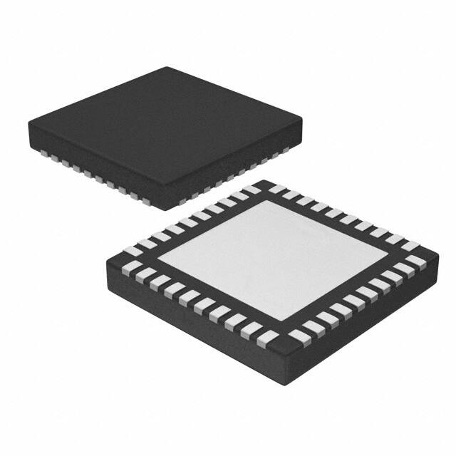


 工商网监
湘ICP备2023018690号
工商网监
湘ICP备2023018690号
