Product
Folder
Sample &
Buy
Support &
Community
Tools &
Software
Technical
Documents
DS125DF111
SNLS450A – JANUARY 2014 – REVISED JUNE 2015
DS125DF111 Multi-Protocol 2-Channel 9.8 - 12.5 Gb/s Retimer
1 Features
3 Description
•
The DS125DF111 is a dual channel (1-lane
bidirectional)
retimer
with
integrated
signal
conditioning. The DS125DF111 includes an input
Continuous-Time Linear Equalizer (CTLE), clock and
data recovery (CDR) and transmit driver on each
channel.
1
•
•
•
•
•
•
•
•
•
•
•
•
•
Pin Compatible Retimer Family
– DS110DF111 with DFE: 8.5 - 11.3 Gbps
– DS125DF111 with DFE: 9.8 - 12.5 Gbps
Adaptive CTLE: 33 dB Max Boost at 6.25 GHz
Self Tuning 5-Tap DFE
Raw Equalized and Retimed Data Loopback
Adjustable Transmit VOD: 600 to 1300 mVp-p
Settable Tx De-Emphasis Driver 0 to –12dB
Low Power Consumption: 220 mW/Channel
Locks to Half/Quarter/Eighth Data Rates for
Legacy Support
On-Chip Eye Monitor (EOM), PRBS Generator
Input Signal Detection, CDR Lock
Detection/Indicator
Single 3.3-V or 2.5-V Power Supply
SMBus, EEPROM, or Pin Based Configuration
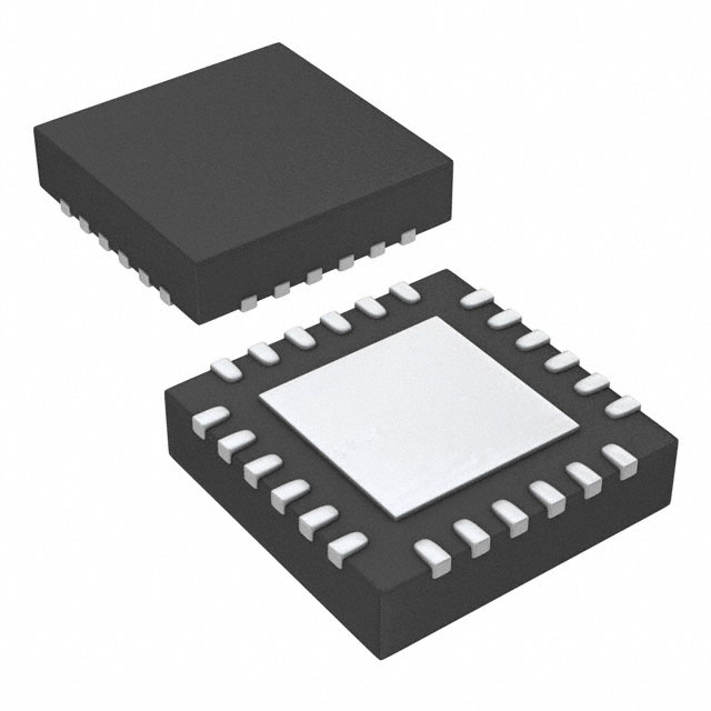
4-mm x 4-mm, 24-Pin WQFN Package
Operating Temp Range: –40°C to 85°C
2 Applications
•
•
•
•
Front Port Optical Interconnects
SFF-8431
10G/1G Ethernet
CPRI
The DS125DF111 with its on-chip Decision Feedback
Equalizer (DFE) can enhance the reach and
robustness of long, lossy, cross-talk-impaired high
speed serial links to achieve BER < 1x10–15. For less
demanding applications/interconnects, the DFE can
be switched off and achieve the same BER
performance. The DS125DF111 and DS110DF111
devices are pin-compatible.
Each channel of the DS125DF111 independently
locks to specific serial data at data rates from 9.8 to
12.5 Gbps or to any supported sub-rate of these data
rates. This simplifies system design and lowers
overall cost.
Programmable transmit de-emphasis driver offers
precise settings to meet the SFF-8431 output eye
template. The fully adaptive receive equalization
(CTLE and DFE) enables longer distance
transmission in lossy copper interconnect and
backplanes with multiple connectors. The CDR
function is ideal for use in front port parallel optical
module applications to reset the jitter budget and
retime high speed serial data.
Device Information(1)
PART NUMBER
DS125DF111
PACKAGE
WQFN (24)
BODY SIZE (NOM)
4.0 mm × 4.0 mm
(1) For all available packages, see the orderable addendum at
the end of the datasheet.
Typical Application
DS125DF111
100nF
OUTA_P
OUTA_N
INA_P
INA_N
100nF
100nF
INB_P
INB_N
25 MHz
2k:
100nF
REFCLK_IN
3.3V
VIN
1�F
GND
0.22�F
(2x)
3.3V
OUTB_P
OUTB_N
VDD
GND
DAP
2k:
SDA
SCL
LPF_REF_B
LPF_CP_B
LPF_REF_A
LPF_CP_A
EN_SMB
TX_DIS
VODA/READ_EN
ADDR0/LOCK
ADDR1/VODB/DONE#
22nF
22nF
3.3V
1k:
1k:
1k:
1k:
1k:
1
An IMPORTANT NOTICE at the end of this data sheet addresses availability, warranty, changes, use in safety-critical applications,
intellectual property matters and other important disclaimers. PRODUCTION DATA.
�DS125DF111
SNLS450A – JANUARY 2014 – REVISED JUNE 2015
www.ti.com
Table of Contents
1
2
3
4
5
6
Features ..................................................................
Applications ...........................................................
Description .............................................................
Revision History.....................................................
Pin Configuration And Functions ........................
Specifications.........................................................
6.1
6.2
6.3
6.4
6.5
6.6
6.7
7
1
1
1
2
3
6
Absolute Maximum Ratings ...................................... 6
ESD Ratings.............................................................. 6
Recommended Operating Conditions....................... 6
Thermal Information .................................................. 6
Electrical Characteristics........................................... 7
Timing Requirements ................................................ 9
Typical Characteristics ............................................ 11
Detailed Description ............................................ 12
7.1 Overview ................................................................. 12
7.2 Functional Block Diagram ....................................... 12
7.3 Feature Description................................................. 12
7.4 Device Functional Modes........................................ 17
7.5 Programming........................................................... 18
7.6 Register Maps ......................................................... 35
8
Application and Implementation ........................ 44
8.1 Application Information............................................ 44
8.2 Typical Application ................................................. 44
9 Power Supply Recommendations...................... 46
10 Layout................................................................... 47
10.1 Layout Guidelines ................................................. 47
10.2 Layout Example .................................................... 47
11 Device and Documentation Support ................. 48
11.1
11.2
11.3
11.4
11.5
Documentation Support ........................................
Community Resources..........................................
Trademarks ...........................................................
Electrostatic Discharge Caution ............................
Glossary ................................................................
48
48
48
48
48
12 Mechanical, Packaging, and Orderable
Information ........................................................... 48
4 Revision History
NOTE: Page numbers for previous revisions may differ from page numbers in the current version.
Changes from Original (January 2014) to Revision A
•
2
Page
Added Pin Configuration and Functions section, Handling Rating table, Feature Description section, Device
Functional Modes, Application and Implementation section, Power Supply Recommendations section, Layout
section, Device and Documentation Support section, and Mechanical, Packaging, and Orderable Information
section ................................................................................................................................................................................... 1
Submit Documentation Feedback
Copyright © 2014–2015, Texas Instruments Incorporated
Product Folder Links: DS125DF111
�DS125DF111
www.ti.com
SNLS450A – JANUARY 2014 – REVISED JUNE 2015
5 Pin Configuration And Functions
TX_DIS/LPBK
SCL/DEMB
SDA/DEMA
ENSMB
LPF_CP_A
LPF_REF_A
6
5
4
3
2
1
RTW Package
24-Pin WQFN
Top View
OUTA+
7
24
INA+
OUTA-
8
23
INA-
VODA/READEN#
9
22
VDD
ADDR1/VODB/DONE#
10
21
VDD
INB+
11
INB-
12
4mm x 4mm, 0.5mm pitch
DAP = GND
13
14
15
16
17
18
LOS/INT#
REFCLK_IN
VIN
ADDR0/LOCK
LPF_CP_B
LPF_REF_B
TOP VIEW
20
OUTB+
19
OUTB-
Pin Functions
PIN
NAME
I/O TYPE
NO.
DESCRIPTION
HIGH SPEED DIFFERENTIAL I/OS
OUTA±
7, 8
O, CML
Inverting and non-inverting CML-compatible differential outputs.
Outputs require AC coupling
OUTB±
20, 19
O, CML
Inverting and non-inverting CML-compatible differential outputs.
Outputs require AC coupling
INA±
24, 23
I, CML
Inverting and non-inverting CML-compatible differential inputs. An onchip 100 Ω terminating resistor connects INA+ to INAInputs require AC coupling. TI recommends 100 nF capacitors. Note that
for SFP+ applications, AC coupling is included as part of the SFP+
module.
INB±
11, 12
I, CML
Inverting and non-inverting CML-compatible differential inputs. An onchip 100 Ω terminating resistor connects INB+ to INBInputs require AC coupling. TI recommends 100 nF capacitors. Note that
for SFP+ applications, AC coupling is included as part of the SFP+
module.
LOOP FILTER CONNECTION PIN
LPF_CP_A, LPF_REF_A
2, 1
I/O, analog
Loop filter connection, place a 22 nF ± 10% capacitor in series between
LPF_CP_A and LPF_REF_A
LPF_CP_B, LPF_REF_B
17, 18
I/O, analog
Loop filter connection, place a 22 nF ± 10% capacitor in series between
LPF_CP_B and LPF_REF_B
14
I, LVCMOS
25 MHz ± 100 ppm clock from external Oscillator
REFERENCE CLOCK I/O
REFCLK_IN
Submit Documentation Feedback
Copyright © 2014–2015, Texas Instruments Incorporated
Product Folder Links: DS125DF111
3
�DS125DF111
SNLS450A – JANUARY 2014 – REVISED JUNE 2015
www.ti.com
Pin Functions (continued)
PIN
NAME
NO.
I/O TYPE
DESCRIPTION
INDICATOR PINS
LOCK
16
O, LVCMOS
LOCK VOH is referenced to VIN voltage level. Note that this pin is shared
with strap input functions read at startup. The Address value loaded into
pin 16 (ADDR0) at startup changes the definition of the LOCK pin output.
See the Shared Register Definition in Table 7 for more details.
LOS/INT#
13
O, Open Drain
Output is driven LOW when a valid signal is present on INA. Output is
released when signal on INA is lost (LOS). This output can be redefined
as an INT# signal which will be driven LOW for any of the following
conditions. (1)
1. The EOM check returns a value below the HEO/VEO interrupt
threshold.
2. CDR check returns lock/loss status.
3. Signal Detector returns detect/loss status.
ENSMB
3
I, 4-Level
System Management Bus (SMBus) enable pin
HIGH = Register Access, SMBus Slave mode
FLOAT = SMBus Master read from External EEPROM
20 K to GND = Reserved
LOW = External Pin Control Mode. See section on Pin Mode Limitation
SDA
4
I, SMBus
O, Open Drain
Data Input / Open Drain Output
External pull-up resistor is required. Pin is 3.3 V LVCMOS tolerant (1)
SCL
5
I, SMBus
O, Open Drain
Clock input in SMBus slave mode. Can also be an open drain output in
SMBus master mode
Pin is 3.3 V LVCMOS Tolerant (1)
TX_DIS
6
I, 4-Level
Disable the OUTB transmitter
HIGH = OUTA Enabled/OUTB Disabled
FLOAT = Reserved
20 K to GND = Reserved
LOW = OUTA/OUTB Enabled (normal operation)
ADDR0
16
I, LVCMOS
This pin sets the SMBus address for the retimer.
This pin is a strap input. The state is read on power-up to set the SMBus
address in SMBus control mode. The latched value of ADDR0 read at
startup will change the LOCK output definition. See the Shared Register
Definition in Table 7 for more details. (2)
ADDR1/DONE#
10
IO, LVCMOS
This pin sets the SMBus address for the retimer in SMBus Slave Mode.
DONE#. VOH is referenced to VIN voltage level. DONE# goes low to
indicate that the SMBus master EEPROM read has been completed in
SMBus Master Mode (2)
READEN#
9
I, LVCMOS
Initiates SMBus master EEPROM read. When multiple DS125DF111 are
connected to a single EEPROM, the READEN# input can be daisy
chained to the DONE# output. In SMBus Slave Mode this pin should be
tied to Logic 0. (3)
SMBus MODE PINS
PIN CONTROL (ENSMB = LOW)
(4)
DEMA
4
I, 4-Level
Set CHA output de-emphasis level in pin control mode
(3)
DEMB
5
I, 4-Level
Set CHB output de-emphasis level in pin control mode
(3)
LPBK
6
I, 4-Level
HIGH = INA goes to OUTA, INB goes to OUTB
FLOAT = INB goes to OUTA and OUTB
20 K to GND = INA goes to OUTA and OUTB
LOW = INA goes to OUTB, INB goes to OUTA (3)
VODA
9
I, 4-Level
Set CHA output launch amplitude in pin control mode
VODB
(1)
(2)
(3)
(4)
4
10
I, 4-Level
Set CHB output launch amplitude in pin control mode
(3)
.
(3)
The LOS/INT# pin is an open drain output which requires external pull-up resistor (typically connected to 2.5 V or 3.3 V for system logic
compatibility) to achieve a HIGH level.
This pin is shared with other functions.
This pin is shared with other functions.
When in pin control mode, the DS125DF111 device operates at 12.288, 9.8304, 6.144, 4.9152, 3.072, 2.4576, 1.536, or 1.2288 Gbps
and has limited VOD and De-Emphasis control. See Table 9.
Submit Documentation Feedback
Copyright © 2014–2015, Texas Instruments Incorporated
Product Folder Links: DS125DF111
�DS125DF111
www.ti.com
SNLS450A – JANUARY 2014 – REVISED JUNE 2015
Pin Functions (continued)
PIN
NAME
I/O TYPE
NO.
DESCRIPTION
POWER
VDD
21, 22
Power
VDD = 2.5 V ± 5%. See Figure 12.
3.3-V supply mode: VDD = 2.5 V is supplied the internal output regulator.
Pins only require de-coupling caps; no external supply is needed.
2.5-V supply mode: VDD input = 2.5 V ± 5%.
VIN
15
Power
Regulator Input (3)with Integrated Supply Mode Control. See Figure 12.
3.3-V supply mode: VIN input = 3.3 V ± 10%.
2.5-V Mode Operation: VIN Supply Input = 2.5 V ± 5%. Connect directly
to VDD supply pins.
DAP
PAD
Power
GND reference
The exposed pad at the center of the package must be connected to
ground plane of the board with at least 4 vias to lower the ground
impedance and improve the thermal performance of the package
Submit Documentation Feedback
Copyright © 2014–2015, Texas Instruments Incorporated
Product Folder Links: DS125DF111
5
�DS125DF111
SNLS450A – JANUARY 2014 – REVISED JUNE 2015
www.ti.com
6 Specifications
6.1 Absolute Maximum Ratings
over operating free-air temperature range (unless otherwise noted)
(1) (2)
MIN
MAX
UNIT
Supply Voltage (VDD)
–0.5
2.75
V
Supply Voltage (VIN)
–0.5
4
V
LVCMOS Input/Output Voltage
–0.5
4
V
4-Level Input Voltage (2.5-V mode)
–0.5
2.75
V
4-Level Input Voltage (3.3-V mode)
–0.5
4
V
SMBus Input/Output Voltage
–0.5
4
V
CML Input Voltage
–0.5
VDD + 0.5
V
CML Input Current
–30
30
mA
Storage temperature, Tstg
–40
125
°C
(1)
(2)
Stresses beyond those listed under Absolute Maximum Ratings may cause permanent damage to the device. These are stress ratings
only, which do not imply functional operation of the device at these or any other conditions beyond those indicated under Recommended
Operating Conditions.
Exposure to absolute-maximum-rated conditions for extended periods may affect device reliability. For soldering specifications, see
product folder at SNOA549.
6.2 ESD Ratings
VALUE
V(ESD)
(1)
(2)
Electrostatic discharge
Human body model (HBM), per ANSI/ESDA/JEDEC JS-001, all
pins (1)
±3000
Charged device model (CDM), per JEDEC specification JESD22C101, all pins (2)
±1500
UNIT
V
JEDEC document JEP155 states that 500-V HBM allows safe manufacturing with a standard ESD control process.
JEDEC document JEP157 states that 250-V CDM allows safe manufacturing with a standard ESD control process.
6.3 Recommended Operating Conditions
MIN
NOM (1)
MAX
2.5 V Mode
2.375
2.5
2.625
3.3 V Mode
3
3.3
3.6
Ambient Temperature
–40
25
+85
°C
SMBus (SDA, SCL) Pull-up Supply Voltage
2.7
3.3
3.6
V
Supply Voltage
(1)
UNIT
V
Typical values represent the most likely parametric norm as determined at the time of design and characterization. Actual typical values
may vary over time and will also depend on the application and configuration.
6.4 Thermal Information
DS125DF111
THERMAL METRIC
(1)
RTW (WQFN)
UNIT
24 PINS
RθJA
Junction-to-ambient thermal resistance
35
°C/W
RθJC(top)
Junction-to-case (top) thermal resistance
34
°C/W
RθJB
Junction-to-board thermal resistance
13.4
°C/W
ψJT
Junction-to-top characterization parameter
0.3
°C/W
ψJB
Junction-to-board characterization parameter
13.4
°C/W
RθJC(bot)
Junction-to-case (bottom) thermal resistance
3.3
°C/W
(1)
6
For more information about traditional and new thermal metrics, see the Semiconductor and IC Package Thermal Metrics application
report, SPRA953.
Submit Documentation Feedback
Copyright © 2014–2015, Texas Instruments Incorporated
Product Folder Links: DS125DF111
�DS125DF111
www.ti.com
SNLS450A – JANUARY 2014 – REVISED JUNE 2015
6.5 Electrical Characteristics
PARAMETER
TEST CONDITIONS
R_Baud
Input baud rate (primary VCO range) Full Rate: DS125DF111
R_Baud2
Divide by 2
Half Rate: DS125DF111
R_Baud4
Divide by 4
Quarter Rate: DS125DF111
R_Baud8
Divide by 8
Eighth Rate: DS125DF111
FSDC
SMBus Clock Rate
REFCLK
Reference Clock Rate
DCREFCLK
Reference Clock Duty Cycle
MIN
TYP (1)
MAX
UNIT
12.5
Gbps
4.9
6.25
Gbps
2.45
3.125
Gbps
Gbps
9.8
1.225
1.5625
Slave Mode Clock Rate
100
400
Master Mode Clock Rate
280
400
40%
50%
± 100 ppm
kHz
520
25
MHz
60%
POWER SUPPLY CURRENT
DS125DF111 Current Consumption
(Whole Device)
IDD
NTps
Supply Noise Tolerance
Average Supply Current, Default
Settings, CHA and CHB Locked
DFE Enabled
175
mA
Average Supply Current, CHA and
CHB Locked
Default Settings except DFE
Disabled
155
mA
Maximum Transient Supply Current
Default Settings: CHA and CHB
valid input signal detected
CHA and CHB acquiring LOCK (2)
294
50 Hz to 100 Hz
100
mVp-p
100 Hz to 10 MHz
40
mVp-p
10 MHz to 3.0 GHz
10
mVp-p
333
mA
LVCMOS (ADDR[1:0], READEN#, REFCLK_IN, DONE#, LOCK)
VIH
High level input voltage
2.5 V or 3.3 V Supply Mode
VIL
Low level input voltage
2.5 V or 3.3 V Supply Mode
VOH1
High level output voltage
IOH = -3 mA
VOH2
High level output voltage
IOH = –100 µA
VOL
Low level output voltage
IOL = 3 mA
IIN
Input leakage current
VINPUT = GND or VIN
1.7
VIN
V
0.7
2
VIN
VIN - 0.1
V
0.4
–15
15
µA
80
µA
4-LEVEL INPUTS (ENSMB, DEMA, DEMB, LPBK, TX_DIS, VODA, VODB)
IIH-R
Input leakage current High
VINPUT = VIN
IIL-R
Input leakage current Low
VINPUT = GND
–160
µA
OPEN DRAIN (LOS/INT#)
VOL
Low level output voltage
IOL = 3 mA
0.4
V
SIGNAL DETECT
SDH
Signal Detect:
ON Threshold Level
Default level to assert
Signal Detect, 12.5 Gbps, PRBS31
18
mVp-p
SDL
Signal Detect:
OFF Threshold Level
Default level to de-assert
Signal Detect, 12.5 Gbps, PRBS31
14
mVp-p
CML RX INPUTS
R_Rd
RLRX-IN
DC Input differential Resistance
Input Return-Loss
80
–19
SDD11 2.0 GHz
–13
SDD11 6.0 - 11.1 GHz
VRX-
Source Transmit Signal Level
LAUNCH
(1)
(2)
(3)
100
SDD11 10 MHz
Tx Launch amplitude of driver
connected to DS125DF111 inputs (3)
Ω
120
dB
-8
1600
mVp-p
Typical values represent the most likely parametric norm as determined at the time of design and characterization. Actual typical values
may vary over time and will also depend on the application and configuration.
Peak current only occurs during lock acquisition, limit is for power supply design not needed for thermal calculations.
DS125DF111 equalizer is optimized to adapt to Tx Launch amplitudes between 600 - 1200 mV. Amplitudes above or below this range
will reduce the overall equalizer performance.
Submit Documentation Feedback
Copyright © 2014–2015, Texas Instruments Incorporated
Product Folder Links: DS125DF111
7
�DS125DF111
SNLS450A – JANUARY 2014 – REVISED JUNE 2015
www.ti.com
Electrical Characteristics (continued)
PARAMETER
TRANSMIT JITTER SPECS
TEST CONDITIONS
MIN
TYP (1)
MAX
UNIT
(4)
TTJ
Total Jitter (@ BER = 1E-12)
PRBS7, 9.8304 Gbps
7.5
ps
TRJ
Random Jitter
PRBS7, 9.8304 Gbps
0.33
ps (RMS)
TDJ
Deterministic Jitter
PRBS7, 9.8304 Gbps
3.6
ps
PLL Bandwidth -3 dB
Measured at 12.5 Gbps, 0.4 UI Sj
Injection
3.9
MHz
Total jitter tolerance
Jitter per SFF-8431 Appendix D.11
Combination of Dj, Pj, and Rj
TLOCK1
TLOCK2
CLOCK AND DATA RECOVERY
BWP
LL
JTOL
> 0.7
UI
CDR Lock Time
Best Lock Time 9.8304 Gbps
Adapt Mode 0 (Register 0x31[6:5])
CTLE Set - no Auto adapt
Disable HEO/VEO Lock Monitor (Register 0x3E[7])
HEO/VEO thresholds set to 0 (Register 0x6A[7:0])
Rate/Subrate limited to single divide
ratio. See Table 9
CDR Reset and Release - (Register
0x0A[3:2])
Signal Detect Preset and Release Before input signal is present
(Register 0x14[7:6])
1.3
ms
CDR Lock Time
Standards Based, 9.8304 Gbps,
Default settings (5)
35
ms
Lock Temperature Range
–40°C to 85°C operating range
125
°C
TEMPLOCK CDR Lock
(4)
(5)
8
Rj and Dj Jitter decomposition as reported by TEK DSA8200 Sampling scope using a 80E09 Electrical sampling module, 80A06 Pattern
trigger, and 82A04 Phase Reference Module.
The typical LOCK time can vary based on data-rate, input channel, and specific DS125DF111 settings.
Submit Documentation Feedback
Copyright © 2014–2015, Texas Instruments Incorporated
Product Folder Links: DS125DF111
�DS125DF111
www.ti.com
SNLS450A – JANUARY 2014 – REVISED JUNE 2015
6.6 Timing Requirements
MIN
NOM
MAX
675
UNIT
CML TX OUTPUTS
T_VDIFF0
Output differential voltage
Default setting, 8T pattern
400
550
Output differential voltage
Maximum setting, 8T
pattern
Requires SMBus Control
1000
1200
mVp-p
VOD_DE
De-emphasis Level
Maximum setting, VOD and
DE
Requires SMBus Control
Input: 9.8304 Gbps, 16T
pattern
–12
dB
T_Rd
DC Output Differential Resistance
T_VDIFF7
mVp-p
100
Ω
Output Rise/Fall Time
Full Slew Rate (Channel
Reg 0x18[2] = 0), minimum
VOD
20% - 80%, See Figure 1.
Input: 9.8304 Gbps, 8T
Pattern
36
ps
TRS/TFS
Output Rise/Fall Time
Limited Slew Rate (Channel
Reg 0x18[2] = 1), minimum
VOD
20% - 80%, See Figure 1.
Input: 9.8304 Gbps, 8T
Pattern
50
ps
TSDD22
Output differential mode return loss
SDD22 10 MHz - 2.0 GHz
–18
dB
1.5UI +
200ps
ps
200
ps
TR/TF
SDD22
5.5 GHz
–11
SDD22 6
- 11.1
GHz
–9
TPD
Propagation Delay
Retimed Data: 9.8304
Gbps,
See Figure 2.
TPD-RAW
Propagation Delay
Raw Data: 9.8304 Gbps,
See Figure 2.
SERIAL BUS INTERFACE CHARACTERISTICS
(1)
See Figure 3.
VIL
Data, Clock Input Low Voltage
(SDA / SCL)
VIH
Data, Clock Input High Voltage
(SDA / SCL)
VOL
Output Low Voltage
SDA or SCL, IOL = 1.25
mA
TR
SDA Rise Time, Read Operation
SDA, RPU = 4.7 K, Cb < 50
pF
140
ns
TF
SDA Fall Time, Read Operation
SDA, RPU = 4.7 K, Cb < 50
pF
60
ns
TSU;DAT
Setup Time, Read Operation
560
ns
THD;DAT
Hold Time, Read Operation
615
ns
CIN
Input Capacitance
TR
SCL and SDA, Rise Time
300
ns
TF
SCL and SDA, Rise Time
1000
ns
(1)
SDA or SCL
0.8
V
2.1
3.6
V
0
0.36
V


 工商网监
湘ICP备2023018690号
工商网监
湘ICP备2023018690号
