DS125DF111EVM Evaluation Board
User's Guide
Literature Number: SNLU158A
January 2014 – Revised January 2016
�Contents
1
2
3
4
5
6
7
8
9
Overview .............................................................................................................................
Features..............................................................................................................................
Applications ........................................................................................................................
Ordering Information ............................................................................................................
Setup ..................................................................................................................................
4
5
5
5
6
5.1
Pin Control Mode ......................................................................................................... 6
5.2
SMBus Slave Mode ...................................................................................................... 9
5.3
EEPROM Mode ......................................................................................................... 12
EVM Layout .......................................................................................................................
Schematic .........................................................................................................................
Bill of Materials ..................................................................................................................
Example Waveforms ...........................................................................................................
13
14
15
16
Revision History .......................................................................................................................... 18
2
Table of Contents
SNLU158A – January 2014 – Revised January 2016
Submit Documentation Feedback
Copyright © 2014–2016, Texas Instruments Incorporated
�www.ti.com
List of Figures
1
DS125DF111EVM ........................................................................................................... 4
2
4-Level I/O Control on DS125DF111EVM ................................................................................ 6
3
DS1xxDF111EVM Slave Mode Full Setup ............................................................................... 9
4
DS1xxDF111EVM Slave Mode Close-Up ................................................................................ 9
5
DS125DF111 High Level Page ........................................................................................... 10
6
DS125DF111 Low Level Page ........................................................................................... 11
7
DS125DF111 Eye Monitor Page ......................................................................................... 11
8
DS125DF111 EEPROM Hex File Generation Page ................................................................... 12
9
Top Assembly Layer ....................................................................................................... 13
10
Bottom Assembly Layer ................................................................................................... 13
11
10.3125 Gbps Output Waveform ......................................................................................... 16
12
10.3125 Gbps Rj/Dj Jitter Decomposition ............................................................................... 17
List of Tables
1
Four-Level Logic Settings................................................................................................... 6
2
DS125DF111 VOD Levels .................................................................................................. 7
3
DS125DF111 DEM Levels.................................................................................................. 7
4
DS125DF111 Loopback Control ........................................................................................... 8
5
SMBus Write Address Assignment
......................................................................................
SNLU158A – January 2014 – Revised January 2016
Submit Documentation Feedback
Copyright © 2014–2016, Texas Instruments Incorporated
List of Figures
10
3
�User's Guide
SNLU158A – January 2014 – Revised January 2016
DS125DF111EVM Evaluation Board
1
Overview
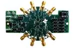
The Texas Instruments DS125DF111EVM evaluation module provides a high bandwidth platform with an
SMA interface to evaluate the DS125DF111 dual channel retimer with integrated signal conditioning. The
DS125DF111 includes an input Continuous-Time Linear Equalizer (CTLE), Clock and Data Recovery
(CDR), and transmit driver on each channel.
Figure 1. DS125DF111EVM
4
DS125DF111EVM Evaluation Board
SNLU158A – January 2014 – Revised January 2016
Submit Documentation Feedback
Copyright © 2014–2016, Texas Instruments Incorporated
�Features
www.ti.com
2
Features
•
•
•
•
•
3
Applications
•
•
•
•
4
Adjustable Transmit VOD: 600 to 1300 mVp-p
Settable Transmit De-emphasis Driver to -12 dB
Low Power Consumption: 200 mW/Channel
Locks to Half/Quarter/Eighth Data Rates for Legacy Support
On-chip Eye Monitor (EOM), PRBS Generator
Front Port Optical Interconnects
SFF-8431
10G/1G Ethernet
CPRI
Ordering Information
EVM ID
DEVICE ID
DEVICE PACKAGE
DS125DF111EVM
DS125DF111SQ
24WQFN
SNLU158A – January 2014 – Revised January 2016
Submit Documentation Feedback
Copyright © 2014–2016, Texas Instruments Incorporated
DS125DF111EVM Evaluation Board
5
�Setup
5
www.ti.com
Setup
This section describes the jumpers and connectors on the EVM as well as how to properly connect, set
up, and use the DS125DF111EVM.
The DS125DF111EVM can be used in three different modes:
1. Pin Control Mode – provides access to selected signal integrity settings.
2. SMBus Slave Mode – provides full access to signal integrity and control settings.
3. EEPROM Mode – provides full access to signal integrity and control settings. EEPROM mode is a
convenient method of programming one or more DS125DF111 devices on system power up when an
SMBus master (microcontroller or similar) is unavailable in the design.
This EVM and documentation focus on Pin Control and SMBus Slave Mode to highlight the ease-of-use
and excellent low-jitter performance of the DS125DF111.
5.1
Pin Control Mode
In Pin Control Mode, the external control pins on the DS125DF111 are used to configure the signal
integrity and control settings of the device. In this mode, only a subset of the VOD and de-emphasis
(DEMA/B) levels are available. Due to the limited number of control pins, a limited bandwidth 4-level input
scheme has been implemented across the control pin interface. This allows for improved DE and VOD
control with fewer physical pins.
The four levels are defined below:
Table 1. Four-Level Logic Settings
Level
Input Pin Setting
Low - 0
1 kΩ to GND
Resistor - R
20 kΩ to GND
Float - F
Open
High - 1
1 kΩ to VDD
The EVM interfaces to this 4-level I/O using the setup in Figure 2. Only one shunt connection is required
to access any of the four levels. This methodology minimizes the risk of improper connections that could
damage the board or board power supply.
4-LEVEL CONTROL
HIGH
RESISTOR
FLOAT
LOW
HIGH
SIGNAL
RESISTOR
SIGNAL
LOW
PIN HEADER CONNECTION
Figure 2. 4-Level I/O Control on DS125DF111EVM
6
DS125DF111EVM Evaluation Board
SNLU158A – January 2014 – Revised January 2016
Submit Documentation Feedback
Copyright © 2014–2016, Texas Instruments Incorporated
�Setup
www.ti.com
5.1.1
Pin Control Mode Configuration
The DS125DF111EVM is shipped ready-to-use in pin control mode. The EVM requires the following power
supply inputs and jumper settings:
1. J17 – GND
2. J19 – VIN to VIH: 3.3 V supply operation (2.5 V internal regulator is enabled)
3. J15 – VIN = 3.3 V: Use internal regulator to convert 3.3V supply to internal supply level of 2.5 V
NOTE: The 2.5 V level may be observed on J18 (VDD) or the device VDD pins. While in 3.3 V mode,
J18 (VDD) is a regulated output voltage. Do not connect a 2.5 V supply to this pin.
4. J3 – ENSMB = 1 kΩ to GND (L): Pin Control Mode
5. J6 – LBK = 1 kΩ to VIN (H): Normal operation, INA - to - OUTA and INB - to - OUTB
6. J91 – VODA = 1 kΩ to GND (L): 600 mV output VOD on OUTA
7. J10 – VODB = 1 kΩ to GND (L): 600 mV output VOD on OUTB
8. J41 – DEMA = 1 kΩ to GND (L): 0 dB de-emphasis on OUTA
9. J51 – DEMB = 1 kΩ to GND (L): 0 dB de-emphasis on OUTB
10. J161 – LOCK: With shunt installed, LOCK LED will light Green when DS125DF111 CDR is in the
locked state
5.1.2
VOD and De-Emphasis
The DS125DF111EVM uses pin strapping to define the VOD and DE level of the outputs. These are set
by the following jumpers on the DS125DF111EVM:
• VODA – J9 / J91
• VODB – J10
• DEMA – J4 / J41
• DEMB – J5 / J51
See Table 2 and Table 3 for a complete list of VOD and DE settings.
Table 2. DS125DF111 VOD Levels
VODA/B
Bit 2,
sel_vod[2]
Bit 1,
sel_vod[1]
Bit 0,
sel_vod[0]
Output VOD (mVppd)
0
0
0
0
600
0
0
1
700
0
1
0
800
0
1
1
900
1
0
0
1000
1
0
1
1100
1
1
0
1200
1
1
1
1300
R
F
1
Table 3. DS125DF111 DEM Levels
DEMA/B
0
R
Reg 0x15
Bit [2]
Reg 0x15
Bit [1]
Reg 0x15
Bit [0]
Reg 0x15
Bit [6]
De-Emphasis (dB)
0
0
0
0
0.0
0
0
1
1
-0.9
0
0
1
0
-1.5
0
1
0
1
-2.0
0
1
1
1
-2.8
1
0
0
1
-3.3
SNLU158A – January 2014 – Revised January 2016
Submit Documentation Feedback
Copyright © 2014–2016, Texas Instruments Incorporated
DS125DF111EVM Evaluation Board
7
�Setup
www.ti.com
Table 3. DS125DF111 DEM Levels (continued)
DEMA/B
F
1
5.1.3
Reg 0x15
Bit [2]
Reg 0x15
Bit [1]
Reg 0x15
Bit [0]
Reg 0x15
Bit [6]
De-Emphasis (dB)
0
1
0
0
-3.5
1
0
1
1
-3.9
1
1
0
1
-4.5
0
1
1
0
-5.0
1
1
1
1
-5.6
1
0
0
0
-6.0
1
0
1
0
-7.5
1
1
0
0
-9.0
1
1
1
0
-12.0
Equalization
There are no pin control settings for the input equalization. The DS125DF111 input equalization will
automatically adapt for divide ratios 1 and 2. For divide ratios 4 and 8, a pre-set equalization level is used.
5.1.4
Loopback
J6 and J61 control the DS125DF111EVM loopback function according to Table 4.
Table 4. DS125DF111 Loopback Control
5.1.5
Loopback
Mode of Operation
IN A
IN B
0
Loopback
Output B
Output A
R
Fanout Input A
Output A
Output A
F
Fanout Input B
Output B
Output B
1
Normal Operation
Output A
Output B
LOS and LOCK
LOS Function: The LOS function monitors the input of channel A for a valid signal. When there is a
valid signal on input A the LED will light up. Channel B does not have any effect on the LOS output
signal.
• LOCK Function: The LOCK function monitors both channel A and channel B for a valid lock condition.
If either channel has a valid lock the LED will light up.
•
8
DS125DF111EVM Evaluation Board
SNLU158A – January 2014 – Revised January 2016
Submit Documentation Feedback
Copyright © 2014–2016, Texas Instruments Incorporated
�Setup
www.ti.com
5.2
SMBus Slave Mode
The SMBus can also be used to control DS125DF111 devices. This method has the advantage of
independent channel control and finer signal conditioning granularity.
1. J17 – GND
2. J19 – VIN to VIH: 3.3 V supply operation (2.5 V internal regulator is enabled)
3. J15 – VIN = 3.3 V: Use internal regulator to convert 3.3 V supply to internal supply level of 2.5 V
NOTE: The 2.5V level may be observed on J18 (VDD) or the device VDD pins. While in 3.3 V mode,
J18 (VDD) is a regulated output voltage. Do not connect a 2.5 V supply to this pin.
4. Floating the AD[1:0] inputs will result in an SMBus address = 00 = 30’h
5. J3 – ENSMB = H: SMBus Slave Mode
6. Connect the board signals SDA, SCL, and GND on J20 to a DPS-DONGLE-EVM or an equivalent
USB2ANY device. A pull-up resistor is needed on the SMBus clock and data signals; place jumpers on
pins 1-2 of J4 and J5 to connect a 1 kΩ pull-up resistor to SCL and SDA. The address line settings on
J16 (ADR0) and J10 (ADR1) are pin strap settings which get latched on power up and retain their
value until the DS125DF111 is power cycled.
7. The DS125DF111's control and signal integrity settings are programmable with SigCon Architect, a
GUI which supports full register access through SMBus communication. An example of a
DS1xxDF111EVM connected to a PC through a DPS-DONGLE-EVM is shown in Figure 3 and
Figure 4. The possible SMBus address settings are shown in Table 5. For more information about
SigCon Architect, reference the "SigCon Architect: Installation and Starter's Guide" (SNLU178).
DS1xxDF111EVM
SMBus Pin Headers
SCL
SDA
GND
PC running either DS110DF111 or
DS125DF111 profile in SigCon Architect
DPS-DONGLE-EVM
SMBus Pin Headers
SCL | SDA | GND
DS1xxDF111EVM
DPS-DONGLE-EVM
Figure 3. DS1xxDF111EVM Slave Mode Full Setup
Figure 4. DS1xxDF111EVM Slave Mode Close-Up
SNLU158A – January 2014 – Revised January 2016
Submit Documentation Feedback
Copyright © 2014–2016, Texas Instruments Incorporated
DS125DF111EVM Evaluation Board
9
�Setup
www.ti.com
Table 5. SMBus Write Address Assignment
(1)
5.2.1
(1)
ADDR1
ADDR0
SMBus Write
SMBus Read
0
0
0x30
0x31
0
1
0x32
0x33
1
0
0x34
0x35
1
1
0x36
0x37
A floating ADDR[1:0] pin at power-up will be interpreted as a logic 0.
Register Architecture and Bit Fields
There are two types of device registers in the DS125DF111. These are the Control/Share Registers and
the Channel Registers. The Control/Share Registers control or allow observation of settings which affect
the operation of all channels of the DS125DF111. They are also used to select which channel of the
device is to be the target channel for reads from and writes to the Channel Registers.
The Channel Registers are used to set all the configuration settings of the DS125DF111. They provide
independent control for each channel of the DS125DF111 for all the configurable device characteristics.
Any registers not described in the datasheet tables should be treated as Reserved. The user should not
try to write new values to these registers. The user-accessible registers described in the datasheet provide
a complete capability for customizing the operation of the DS125DF111 on a channel-by-channel basis.
Many of the registers in the DS125DF111 are divided into bit fields. This allows a single register to serve
multiple purposes, which may be unrelated. Often configuring the DS125DF111 requires writing a bit field
that makes up only part of a register value while leaving the remainder of the register value unchanged.
5.2.2
Using SigCon Architect
SigCon Architect can be used to program the DS125DF111EVM. In order to use SigCon Architect for
SMBus Slave Mode access control, a DPS-DONGLE-EVM (see SNLU184) or USB2ANY equivalent
adapter board must be used. This adapter board serves as an interface board to allow SMBus
communication between the PC and the DS125DF111 retimer. The SigCon Architect GUI features high
level control, low level register bit level control, and an Eye Monitor page to program the device. Examples
of these pages are shown in the following figures.
Figure 5. DS125DF111 High Level Page
10
DS125DF111EVM Evaluation Board
SNLU158A – January 2014 – Revised January 2016
Submit Documentation Feedback
Copyright © 2014–2016, Texas Instruments Incorporated
�Setup
www.ti.com
Figure 6. DS125DF111 Low Level Page
Figure 7. DS125DF111 Eye Monitor Page
For more information about functions about SigCon Architect and the retimer profiles, please reference the
"SigCon Architect: Installation and Starter's Guide" (SNLU178) and the "DS110DF410EVK,
DS110DF410EVK, and DS125DF410EVM Evaluation Board Software Installation, Setup, and Operating
Guide" (SNLU126).
SNLU158A – January 2014 – Revised January 2016
Submit Documentation Feedback
Copyright © 2014–2016, Texas Instruments Incorporated
DS125DF111EVM Evaluation Board
11
�Setup
5.3
www.ti.com
EEPROM Mode
A serial EEPROM may also be used to configure one or more DS125DF111 devices. This configuration
mode is accessed by setting ENSMB = FLOAT. When the DS125DF111 is placed in EEPROM Mode, the
DS125DF111 will attempt to load its startup settings from a programmed EEPROM in the 8-pin DIP socket
(U2). SigCon Architect can be used to generate an EEPROM Hex file by configuring the EEPROM page
settings.
Figure 8. DS125DF111 EEPROM Hex File Generation Page
SigCon Architect cannot directly program the EEPROM. A third-party tool must be used to write the
EEPROM hex file into a valid EEPROM. For details about EEPROM hex file generation, please reference
"Understanding EEPROM Programming for 10G to 12.5G Retimers" (SNLA245) and the
"DS110DF410EVK, DS110DF410EVK, and DS125DF410EVM Evaluation Board Software Installation,
Setup, and Operating Guide" (SNLU126).
12
DS125DF111EVM Evaluation Board
SNLU158A – January 2014 – Revised January 2016
Submit Documentation Feedback
Copyright © 2014–2016, Texas Instruments Incorporated
�EVM Layout
www.ti.com
6
EVM Layout
Figure 9 and Figure 10 show the board layout for the DS125DF111EVM. The EVM uses simple 100 mil
headers to control the output signal integrity functions. The DS125DF111EVM is very compact and low
power. The board traces have been designed for connection to standard 50 Ω test equipment and cables.
The QFN package offers an exposed thermal pad to enhance electrical and thermal performance (this pad
must be soldered to the copper landing on the PCB).
Figure 9. Top Assembly Layer
Figure 10. Bottom Assembly Layer
SNLU158A – January 2014 – Revised January 2016
Submit Documentation Feedback
Copyright © 2014–2016, Texas Instruments Incorporated
DS125DF111EVM Evaluation Board
13
�Schematic
7
www.ti.com
Schematic
R1
1K
VIH
1
3
5
VIH
R7
1K
2
4
6
R4
1K
ADDR1
TX_DIS
R2
20K
J10
WM8121-ND
R3
1K
C1
SIG
C2
0.1u
1
IN B
0.1u
SIG
1
2
3
1
2
3
1
2
3
1
2
3
VODA
SCL
SDA
ENSMB
C4
0.1u
1
WM6503-ND
24
23
22
21
20
19
SIG
25
1
2
R11
20K
J91
VODA
WM6502-ND
1
2
WM6503-ND
J51
WM6502-ND
R17
1K
GND
1
2
SCL
J41
R12
1K
2
3
4
5
GND
GND
GND
GND
WM6502-ND
R15
1K
GND
J17
VDD
C7
0.1u
J18
J19
C11
0.22
C12
0.22
1
2
VDD
VDD
SIG
2
3
4
5
GND
GND
GND
GND
1287-ST
1287-ST
WM6503-ND
142-0771-821
OUT B
J15
C8
0.1u
SMA8
1
SIG
2
3
4
5
GND
GND
GND
GND
VIH
1
2
VIN
VIN
PLACE AT J15
142-0771-821
PLACE AT U1
VIH
C14
10u
C15
0.1u
A2
20K
1
2
REFCLK
0
J141
U3
EN
1
2
R26
20K
J14
EN
VDD
GND
OUT
1
3
5
VIH
R23
1
2
4
3
2
4
6
R29
GND
8-PIN DIP SOCKET for AT24C01B EEPROM
U2
ADDR0
J16
WM8121-ND
R20
50 (DNP)
R33
1K
R35
1K
1K
GND
OSC
R34
DNP
WP
R31
1K
ADDR0
R25
R32
DNP
1287-ST
A1
VIN
VIH
R30
DNP
REFCLK
VIH
1
2
3
VDD
VIH
VIN
SMA7
1
142-0771-821
R24
GND
1
2
SDA
WM6502-ND
R6
1K
WM6503-ND
R14
20K
GND
1
2
C10
0.022u
LOS
TX_DIS
GND
142-0771-821
PLACE AT U1
DAP
2
3
4
5
GND
GND
GND
GND
WM6503-ND
R5
20K
J61
SMA6
13
14
15
16
17
18
SMA4
GND
GND
GND
GND
VODA
ADDR1
0.1u
1
142-0771-821
2
3
4
5
J3
1
2
3
R9
1K
1
OUTA+
INA+
OUTAINAVODA/READEN#
VDD
ADDR1/VODB/DONE#
VDD
INB+
OUTB+
INBOUTB-
LOS/INT#
REFCLK_IN
VIN
ADDR0/LOCK
LPF_CP_B
LPF_REF_B
SIG
C3
7
8
9
10
11
12
GND
142-0771-821
IN A
C6
SIG
DS125DF111
SMA3
GND
GND
GND
GND
6
5
4
3
2
1
U1
OUT A
142-0771-821
2
3
4
5
SMA5
1
TX_DIS/LBK
SCL/DEMB
SDA/DEMA
ENSMB
LPF_CP_A
LPF_REF_A
GND
GND
GND
GND
0.1u
C9
0.022u
SMA2
2
3
4
5
C5
1
142-0771-821
J4
R8
20K
0.1u
TX_DIS
SIG
R16
1K
J5
WM6503-ND
SDA
SCL
GND
GND
GND
GND
R13
1K
J9
ENSMB
SMA1
2
3
4
5
R10
1K
J6
GND
A1
A2
1
2
3
GND
4
1K
A0
A1
A2
GND
VCC
WP
SCL
SDA
8
VIH
7
6
5
WP
SCL
SDA
GND
J20
SCL
SDA
GND
C16
0.1u
1
2
3
WM6503-ND
4808-3004-CP
WM6502-ND
WM6502-ND
535-11750-1-ND
25 MHz Oscillator
LOCKED = ON (GREEN)
R27
C13
0.1u
ADDR0
220
GND
D1 SML-310PTT86
J161
1
2
WM6502-ND
LOSS of SIGNAL = ON (GREEN)
R28
220
VIH
LOS
D2 SML-310PTT86
14
DS125DF111EVM Evaluation Board
SNLU158A – January 2014 – Revised January 2016
Submit Documentation Feedback
Copyright © 2014–2016, Texas Instruments Incorporated
�Bill of Materials
www.ti.com
8
Bill of Materials
Qty
Reference Designator
Description
Manufacturer
Part Number
1
PCB
DS125DF111EVM PCB
Texas Instruments
SV601028
11
C1, C2, C3, C4, C5, C6,
C7, C8, C13, C15, C16
CAP CER 0.1UF 10V 10% X5R 0201
Taiyo Yuden
LMK063BJ104KP-F
2
C9, C10
CAP CER 0.022UF 6.3V 10% X5R 0201
TDK
C0603X5R0J223K030BC
2
C11, C12
CAP CER 0.22UF 10V 20% X5R 0201
Taiyo Yuden
LMK063BJ224MP-F
1
C14
CAP CER 10UF 6.3V 20% X5R 0603
TDK
C1608X5R0J106M080AB
2
D1, D2
LED GREEN 0.2MM 13MCD 0402 SMD
Rohm
SML-310PTT86
7
J3, J4, J5, J6, J9, J19,
J20
CONN HEADER 3POS .100 VERT GOLD
Molex
22-28-4033
2
J10, J16
CONN HEADER 6POS .100" STR TIN
Molex
90131-0123
7
J14, J41, J51, J61, J91,
J141, J161
CONN HEADER 2POS .100 VERT GOLD
Molex
22-28-4023
3
J15, J17, J18
TERM QF .052"DIA .250" STURDY MT
Keystone
1287-ST
17
R1, R3, R4, R6, R7, R9,
R10, R12, R13, R15,
R16, R17, R25, R29,
R31, R33, R35
RES 1K OHM 1/16W 5% 0402 SMD
Rohm
MCR01MZPJ102
7
R2, R5, R8, R11, R14,
R24, R26
RES 20K OHM 1/10W 5% 0402 SMD
Panasonic
ERJ-2GEJ203X
1
R23
RES 0.0 OHM 1/10W JUMP 0402 SMD
Panasonic
ERJ-2GE0R00X
2
R27, R28
RES 220 OHM 1/16W 5% 0402 SMD
Rohm
MCR01MZPJ221
8
SMA1, SMA2, SMA3,
SMA4, SMA5, SMA6,
SMA7, SMA8
CONN SMA JACK 50 OHM EDGE MNT
Emerson
142-0771-821
1
U1
RETIMER
Texas Instruments
DS125DF111SQ
1
U2
SOCKET IC OPEN FRAME 8POS .3"
3M
4808-3004-CP
1
U3
OSC MEMS 25.000 MHZ SMD
Abracon
ASEMB-25.000MHZ-LC-T
CONN JUMPER SHORTING GOLD FLASH
Sullins
SPC02SYAN
8
SNLU158A – January 2014 – Revised January 2016
Submit Documentation Feedback
Copyright © 2014–2016, Texas Instruments Incorporated
DS125DF111EVM Evaluation Board
15
�Example Waveforms
9
www.ti.com
Example Waveforms
With the default power up configuration, the DS125DF111 is designed to lock to 12.288, 9.8304, 6.144,
4.9152, 3.072, 2.4576, 1.536, and 1.2288 Gbps encoded data. The results in Figure 11 and Figure 12 are
typical when measured and observed via test equipment attached to the EVM with matched SMA coaxial
cables.
Figure 11. 10.3125 Gbps Output Waveform
16
DS125DF111EVM Evaluation Board
SNLU158A – January 2014 – Revised January 2016
Submit Documentation Feedback
Copyright © 2014–2016, Texas Instruments Incorporated
�Example Waveforms
www.ti.com
Figure 12. 10.3125 Gbps Rj/Dj Jitter Decomposition
SNLU158A – January 2014 – Revised January 2016
Submit Documentation Feedback
Copyright © 2014–2016, Texas Instruments Incorporated
DS125DF111EVM Evaluation Board
17
�Revision History
www.ti.com
Revision History
Changes from Original (January 2014) to A Revision .................................................................................................... Page
•
•
•
•
•
•
Added Features, Applications, and Ordering Information contents ................................................................. 5
Changed source formatting of Pin Control descriptions .............................................................................. 6
Changed connection to reflect operation with SigCon Architect through the DPS-DONGLE-EVM adapter board........... 9
Added new subsections for register archtiecture and SigCon Architect basics ................................................. 10
Added detailed description about operation in EEPROM mode ................................................................... 12
Changed display format of EVM layout ............................................................................................... 13
NOTE: Page numbers for previous revisions may differ from page numbers in the current version.
18
Revision History
SNLU158A – January 2014 – Revised January 2016
Submit Documentation Feedback
Copyright © 2014–2016, Texas Instruments Incorporated
�STANDARD TERMS AND CONDITIONS FOR EVALUATION MODULES
1.
Delivery: TI delivers TI evaluation boards, kits, or modules, including demonstration software, components, and/or documentation
which may be provided together or separately (collectively, an “EVM” or “EVMs”) to the User (“User”) in accordance with the terms
and conditions set forth herein. Acceptance of the EVM is expressly subject to the following terms and conditions.
1.1 EVMs are intended solely for product or software developers for use in a research and development setting to facilitate feasibility
evaluation, experimentation, or scientific analysis of TI semiconductors products. EVMs have no direct function and are not
finished products. EVMs shall not be directly or indirectly assembled as a part or subassembly in any finished product. For
clarification, any software or software tools provided with the EVM (“Software”) shall not be subject to the terms and conditions
set forth herein but rather shall be subject to the applicable terms and conditions that accompany such Software
1.2 EVMs are not intended for consumer or household use. EVMs may not be sold, sublicensed, leased, rented, loaned, assigned,
or otherwise distributed for commercial purposes by Users, in whole or in part, or used in any finished product or production
system.
2
Limited Warranty and Related Remedies/Disclaimers:
2.1 These terms and conditions do not apply to Software. The warranty, if any, for Software is covered in the applicable Software
License Agreement.
2.2 TI warrants that the TI EVM will conform to TI's published specifications for ninety (90) days after the date TI delivers such EVM
to User. Notwithstanding the foregoing, TI shall not be liable for any defects that are caused by neglect, misuse or mistreatment
by an entity other than TI, including improper installation or testing, or for any EVMs that have been altered or modified in any
way by an entity other than TI. Moreover, TI shall not be liable for any defects that result from User's design, specifications or
instructions for such EVMs. Testing and other quality control techniques are used to the extent TI deems necessary or as
mandated by government requirements. TI does not test all parameters of each EVM.
2.3 If any EVM fails to conform to the warranty set forth above, TI's sole liability shall be at its option to repair or replace such EVM,
or credit User's account for such EVM. TI's liability under this warranty shall be limited to EVMs that are returned during the
warranty period to the address designated by TI and that are determined by TI not to conform to such warranty. If TI elects to
repair or replace such EVM, TI shall have a reasonable time to repair such EVM or provide replacements. Repaired EVMs shall
be warranted for the remainder of the original warranty period. Replaced EVMs shall be warranted for a new full ninety (90) day
warranty period.
3
Regulatory Notices:
3.1 United States
3.1.1
Notice applicable to EVMs not FCC-Approved:
This kit is designed to allow product developers to evaluate electronic components, circuitry, or software associated with the kit
to determine whether to incorporate such items in a finished product and software developers to write software applications for
use with the end product. This kit is not a finished product and when assembled may not be resold or otherwise marketed unless
all required FCC equipment authorizations are first obtained. Operation is subject to the condition that this product not cause
harmful interference to licensed radio stations and that this product accept harmful interference. Unless the assembled kit is
designed to operate under part 15, part 18 or part 95 of this chapter, the operator of the kit must operate under the authority of
an FCC license holder or must secure an experimental authorization under part 5 of this chapter.
3.1.2
For EVMs annotated as FCC – FEDERAL COMMUNICATIONS COMMISSION Part 15 Compliant:
CAUTION
This device complies with part 15 of the FCC Rules. Operation is subject to the following two conditions: (1) This device may not
cause harmful interference, and (2) this device must accept any interference received, including interference that may cause
undesired operation.
Changes or modifications not expressly approved by the party responsible for compliance could void the user's authority to
operate the equipment.
FCC Interference Statement for Class A EVM devices
NOTE: This equipment has been tested and found to comply with the limits for a Class A digital device, pursuant to part 15 of
the FCC Rules. These limits are designed to provide reasonable protection against harmful interference when the equipment is
operated in a commercial environment. This equipment generates, uses, and can radiate radio frequency energy and, if not
installed and used in accordance with the instruction manual, may cause harmful interference to radio communications.
Operation of this equipment in a residential area is likely to cause harmful interference in which case the user will be required to
correct the interference at his own expense.
SPACER
SPACER
SPACER
SPACER
SPACER
SPACER
SPACER
SPACER
�FCC Interference Statement for Class B EVM devices
NOTE: This equipment has been tested and found to comply with the limits for a Class B digital device, pursuant to part 15 of
the FCC Rules. These limits are designed to provide reasonable protection against harmful interference in a residential
installation. This equipment generates, uses and can radiate radio frequency energy and, if not installed and used in accordance
with the instructions, may cause harmful interference to radio communications. However, there is no guarantee that interference
will not occur in a particular installation. If this equipment does cause harmful interference to radio or television reception, which
can be determined by turning the equipment off and on, the user is encouraged to try to correct the interference by one or more
of the following measures:
•
•
•
•
Reorient or relocate the receiving antenna.
Increase the separation between the equipment and receiver.
Connect the equipment into an outlet on a circuit different from that to which the receiver is connected.
Consult the dealer or an experienced radio/TV technician for help.
3.2 Canada
3.2.1
For EVMs issued with an Industry Canada Certificate of Conformance to RSS-210
Concerning EVMs Including Radio Transmitters:
This device complies with Industry Canada license-exempt RSS standard(s). Operation is subject to the following two conditions:
(1) this device may not cause interference, and (2) this device must accept any interference, including interference that may
cause undesired operation of the device.
Concernant les EVMs avec appareils radio:
Le présent appareil est conforme aux CNR d'Industrie Canada applicables aux appareils radio exempts de licence. L'exploitation
est autorisée aux deux conditions suivantes: (1) l'appareil ne doit pas produire de brouillage, et (2) l'utilisateur de l'appareil doit
accepter tout brouillage radioélectrique subi, même si le brouillage est susceptible d'en compromettre le fonctionnement.
Concerning EVMs Including Detachable Antennas:
Under Industry Canada regulations, this radio transmitter may only operate using an antenna of a type and maximum (or lesser)
gain approved for the transmitter by Industry Canada. To reduce potential radio interference to other users, the antenna type
and its gain should be so chosen that the equivalent isotropically radiated power (e.i.r.p.) is not more than that necessary for
successful communication. This radio transmitter has been approved by Industry Canada to operate with the antenna types
listed in the user guide with the maximum permissible gain and required antenna impedance for each antenna type indicated.
Antenna types not included in this list, having a gain greater than the maximum gain indicated for that type, are strictly prohibited
for use with this device.
Concernant les EVMs avec antennes détachables
Conformément à la réglementation d'Industrie Canada, le présent émetteur radio peut fonctionner avec une antenne d'un type et
d'un gain maximal (ou inférieur) approuvé pour l'émetteur par Industrie Canada. Dans le but de réduire les risques de brouillage
radioélectrique à l'intention des autres utilisateurs, il faut choisir le type d'antenne et son gain de sorte que la puissance isotrope
rayonnée équivalente (p.i.r.e.) ne dépasse pas l'intensité nécessaire à l'établissement d'une communication satisfaisante. Le
présent émetteur radio a été approuvé par Industrie Canada pour fonctionner avec les types d'antenne énumérés dans le
manuel d’usage et ayant un gain admissible maximal et l'impédance requise pour chaque type d'antenne. Les types d'antenne
non inclus dans cette liste, ou dont le gain est supérieur au gain maximal indiqué, sont strictement interdits pour l'exploitation de
l'émetteur
3.3 Japan
3.3.1
Notice for EVMs delivered in Japan: Please see http://www.tij.co.jp/lsds/ti_ja/general/eStore/notice_01.page 日本国内に
輸入される評価用キット、ボードについては、次のところをご覧ください。
http://www.tij.co.jp/lsds/ti_ja/general/eStore/notice_01.page
3.3.2
Notice for Users of EVMs Considered “Radio Frequency Products” in Japan: EVMs entering Japan may not be certified
by TI as conforming to Technical Regulations of Radio Law of Japan.
If User uses EVMs in Japan, not certified to Technical Regulations of Radio Law of Japan, User is required by Radio Law of
Japan to follow the instructions below with respect to EVMs:
1.
2.
3.
Use EVMs in a shielded room or any other test facility as defined in the notification #173 issued by Ministry of Internal
Affairs and Communications on March 28, 2006, based on Sub-section 1.1 of Article 6 of the Ministry’s Rule for
Enforcement of Radio Law of Japan,
Use EVMs only after User obtains the license of Test Radio Station as provided in Radio Law of Japan with respect to
EVMs, or
Use of EVMs only after User obtains the Technical Regulations Conformity Certification as provided in Radio Law of Japan
with respect to EVMs. Also, do not transfer EVMs, unless User gives the same notice above to the transferee. Please note
that if User does not follow the instructions above, User will be subject to penalties of Radio Law of Japan.
SPACER
SPACER
SPACER
SPACER
SPACER
�【無線電波を送信する製品の開発キットをお使いになる際の注意事項】 開発キットの中には技術基準適合証明を受けて
いないものがあります。 技術適合証明を受けていないもののご使用に際しては、電波法遵守のため、以下のいずれかの
措置を取っていただく必要がありますのでご注意ください。
1.
2.
3.
電波法施行規則第6条第1項第1号に基づく平成18年3月28日総務省告示第173号で定められた電波暗室等の試験設備でご使用
いただく。
実験局の免許を取得後ご使用いただく。
技術基準適合証明を取得後ご使用いただく。
なお、本製品は、上記の「ご使用にあたっての注意」を譲渡先、移転先に通知しない限り、譲渡、移転できないものとします。
上記を遵守頂けない場合は、電波法の罰則が適用される可能性があることをご留意ください。 日本テキサス・イ
ンスツルメンツ株式会社
東京都新宿区西新宿6丁目24番1号
西新宿三井ビル
3.3.3
Notice for EVMs for Power Line Communication: Please see http://www.tij.co.jp/lsds/ti_ja/general/eStore/notice_02.page
電力線搬送波通信についての開発キットをお使いになる際の注意事項については、次のところをご覧ください。http:/
/www.tij.co.jp/lsds/ti_ja/general/eStore/notice_02.page
SPACER
4
EVM Use Restrictions and Warnings:
4.1 EVMS ARE NOT FOR USE IN FUNCTIONAL SAFETY AND/OR SAFETY CRITICAL EVALUATIONS, INCLUDING BUT NOT
LIMITED TO EVALUATIONS OF LIFE SUPPORT APPLICATIONS.
4.2 User must read and apply the user guide and other available documentation provided by TI regarding the EVM prior to handling
or using the EVM, including without limitation any warning or restriction notices. The notices contain important safety information
related to, for example, temperatures and voltages.
4.3 Safety-Related Warnings and Restrictions:
4.3.1
User shall operate the EVM within TI’s recommended specifications and environmental considerations stated in the user
guide, other available documentation provided by TI, and any other applicable requirements and employ reasonable and
customary safeguards. Exceeding the specified performance ratings and specifications (including but not limited to input
and output voltage, current, power, and environmental ranges) for the EVM may cause personal injury or death, or
property damage. If there are questions concerning performance ratings and specifications, User should contact a TI
field representative prior to connecting interface electronics including input power and intended loads. Any loads applied
outside of the specified output range may also result in unintended and/or inaccurate operation and/or possible
permanent damage to the EVM and/or interface electronics. Please consult the EVM user guide prior to connecting any
load to the EVM output. If there is uncertainty as to the load specification, please contact a TI field representative.
During normal operation, even with the inputs and outputs kept within the specified allowable ranges, some circuit
components may have elevated case temperatures. These components include but are not limited to linear regulators,
switching transistors, pass transistors, current sense resistors, and heat sinks, which can be identified using the
information in the associated documentation. When working with the EVM, please be aware that the EVM may become
very warm.
4.3.2
EVMs are intended solely for use by technically qualified, professional electronics experts who are familiar with the
dangers and application risks associated with handling electrical mechanical components, systems, and subsystems.
User assumes all responsibility and liability for proper and safe handling and use of the EVM by User or its employees,
affiliates, contractors or designees. User assumes all responsibility and liability to ensure that any interfaces (electronic
and/or mechanical) between the EVM and any human body are designed with suitable isolation and means to safely
limit accessible leakage currents to minimize the risk of electrical shock hazard. User assumes all responsibility and
liability for any improper or unsafe handling or use of the EVM by User or its employees, affiliates, contractors or
designees.
4.4 User assumes all responsibility and liability to determine whether the EVM is subject to any applicable international, federal,
state, or local laws and regulations related to User’s handling and use of the EVM and, if applicable, User assumes all
responsibility and liability for compliance in all respects with such laws and regulations. User assumes all responsibility and
liability for proper disposal and recycling of the EVM consistent with all applicable international, federal, state, and local
requirements.
5.
Accuracy of Information: To the extent TI provides information on the availability and function of EVMs, TI attempts to be as accurate
as possible. However, TI does not warrant the accuracy of EVM descriptions, EVM availability or other information on its websites as
accurate, complete, reliable, current, or error-free.
SPACER
SPACER
SPACER
SPACER
SPACER
SPACER
�SPACER
6.
Disclaimers:
6.1 EXCEPT AS SET FORTH ABOVE, EVMS AND ANY WRITTEN DESIGN MATERIALS PROVIDED WITH THE EVM (AND THE
DESIGN OF THE EVM ITSELF) ARE PROVIDED "AS IS" AND "WITH ALL FAULTS." TI DISCLAIMS ALL OTHER
WARRANTIES, EXPRESS OR IMPLIED, REGARDING SUCH ITEMS, INCLUDING BUT NOT LIMITED TO ANY IMPLIED
WARRANTIES OF MERCHANTABILITY OR FITNESS FOR A PARTICULAR PURPOSE OR NON-INFRINGEMENT OF ANY
THIRD PARTY PATENTS, COPYRIGHTS, TRADE SECRETS OR OTHER INTELLECTUAL PROPERTY RIGHTS.
6.2 EXCEPT FOR THE LIMITED RIGHT TO USE THE EVM SET FORTH HEREIN, NOTHING IN THESE TERMS AND
CONDITIONS SHALL BE CONSTRUED AS GRANTING OR CONFERRING ANY RIGHTS BY LICENSE, PATENT, OR ANY
OTHER INDUSTRIAL OR INTELLECTUAL PROPERTY RIGHT OF TI, ITS SUPPLIERS/LICENSORS OR ANY OTHER THIRD
PARTY, TO USE THE EVM IN ANY FINISHED END-USER OR READY-TO-USE FINAL PRODUCT, OR FOR ANY
INVENTION, DISCOVERY OR IMPROVEMENT MADE, CONCEIVED OR ACQUIRED PRIOR TO OR AFTER DELIVERY OF
THE EVM.
7.
USER'S INDEMNITY OBLIGATIONS AND REPRESENTATIONS. USER WILL DEFEND, INDEMNIFY AND HOLD TI, ITS
LICENSORS AND THEIR REPRESENTATIVES HARMLESS FROM AND AGAINST ANY AND ALL CLAIMS, DAMAGES, LOSSES,
EXPENSES, COSTS AND LIABILITIES (COLLECTIVELY, "CLAIMS") ARISING OUT OF OR IN CONNECTION WITH ANY
HANDLING OR USE OF THE EVM THAT IS NOT IN ACCORDANCE WITH THESE TERMS AND CONDITIONS. THIS OBLIGATION
SHALL APPLY WHETHER CLAIMS ARISE UNDER STATUTE, REGULATION, OR THE LAW OF TORT, CONTRACT OR ANY
OTHER LEGAL THEORY, AND EVEN IF THE EVM FAILS TO PERFORM AS DESCRIBED OR EXPECTED.
8.
Limitations on Damages and Liability:
8.1 General Limitations. IN NO EVENT SHALL TI BE LIABLE FOR ANY SPECIAL, COLLATERAL, INDIRECT, PUNITIVE,
INCIDENTAL, CONSEQUENTIAL, OR EXEMPLARY DAMAGES IN CONNECTION WITH OR ARISING OUT OF THESE
TERMS ANDCONDITIONS OR THE USE OF THE EVMS PROVIDED HEREUNDER, REGARDLESS OF WHETHER TI HAS
BEEN ADVISED OF THE POSSIBILITY OF SUCH DAMAGES. EXCLUDED DAMAGES INCLUDE, BUT ARE NOT LIMITED
TO, COST OF REMOVAL OR REINSTALLATION, ANCILLARY COSTS TO THE PROCUREMENT OF SUBSTITUTE GOODS
OR SERVICES, RETESTING, OUTSIDE COMPUTER TIME, LABOR COSTS, LOSS OF GOODWILL, LOSS OF PROFITS,
LOSS OF SAVINGS, LOSS OF USE, LOSS OF DATA, OR BUSINESS INTERRUPTION. NO CLAIM, SUIT OR ACTION SHALL
BE BROUGHT AGAINST TI MORE THAN ONE YEAR AFTER THE RELATED CAUSE OF ACTION HAS OCCURRED.
8.2 Specific Limitations. IN NO EVENT SHALL TI'S AGGREGATE LIABILITY FROM ANY WARRANTY OR OTHER OBLIGATION
ARISING OUT OF OR IN CONNECTION WITH THESE TERMS AND CONDITIONS, OR ANY USE OF ANY TI EVM
PROVIDED HEREUNDER, EXCEED THE TOTAL AMOUNT PAID TO TI FOR THE PARTICULAR UNITS SOLD UNDER
THESE TERMS AND CONDITIONS WITH RESPECT TO WHICH LOSSES OR DAMAGES ARE CLAIMED. THE EXISTENCE
OF MORE THAN ONE CLAIM AGAINST THE PARTICULAR UNITS SOLD TO USER UNDER THESE TERMS AND
CONDITIONS SHALL NOT ENLARGE OR EXTEND THIS LIMIT.
9.
Return Policy. Except as otherwise provided, TI does not offer any refunds, returns, or exchanges. Furthermore, no return of EVM(s)
will be accepted if the package has been opened and no return of the EVM(s) will be accepted if they are damaged or otherwise not in
a resalable condition. If User feels it has been incorrectly charged for the EVM(s) it ordered or that delivery violates the applicable
order, User should contact TI. All refunds will be made in full within thirty (30) working days from the return of the components(s),
excluding any postage or packaging costs.
10. Governing Law: These terms and conditions shall be governed by and interpreted in accordance with the laws of the State of Texas,
without reference to conflict-of-laws principles. User agrees that non-exclusive jurisdiction for any dispute arising out of or relating to
these terms and conditions lies within courts located in the State of Texas and consents to venue in Dallas County, Texas.
Notwithstanding the foregoing, any judgment may be enforced in any United States or foreign court, and TI may seek injunctive relief
in any United States or foreign court.
Mailing Address: Texas Instruments, Post Office Box 655303, Dallas, Texas 75265
Copyright © 2016, Texas Instruments Incorporated
spacer
�IMPORTANT NOTICE
Texas Instruments Incorporated and its subsidiaries (TI) reserve the right to make corrections, enhancements, improvements and other
changes to its semiconductor products and services per JESD46, latest issue, and to discontinue any product or service per JESD48, latest
issue. Buyers should obtain the latest relevant information before placing orders and should verify that such information is current and
complete. All semiconductor products (also referred to herein as “components”) are sold subject to TI’s terms and conditions of sale
supplied at the time of order acknowledgment.
TI warrants performance of its components to the specifications applicable at the time of sale, in accordance with the warranty in TI’s terms
and conditions of sale of semiconductor products. Testing and other quality control techniques are used to the extent TI deems necessary
to support this warranty. Except where mandated by applicable law, testing of all parameters of each component is not necessarily
performed.
TI assumes no liability for applications assistance or the design of Buyers’ products. Buyers are responsible for their products and
applications using TI components. To minimize the risks associated with Buyers’ products and applications, Buyers should provide
adequate design and operating safeguards.
TI does not warrant or represent that any license, either express or implied, is granted under any patent right, copyright, mask work right, or
other intellectual property right relating to any combination, machine, or process in which TI components or services are used. Information
published by TI regarding third-party products or services does not constitute a license to use such products or services or a warranty or
endorsement thereof. Use of such information may require a license from a third party under the patents or other intellectual property of the
third party, or a license from TI under the patents or other intellectual property of TI.
Reproduction of significant portions of TI information in TI data books or data sheets is permissible only if reproduction is without alteration
and is accompanied by all associated warranties, conditions, limitations, and notices. TI is not responsible or liable for such altered
documentation. Information of third parties may be subject to additional restrictions.
Resale of TI components or services with statements different from or beyond the parameters stated by TI for that component or service
voids all express and any implied warranties for the associated TI component or service and is an unfair and deceptive business practice.
TI is not responsible or liable for any such statements.
Buyer acknowledges and agrees that it is solely responsible for compliance with all legal, regulatory and safety-related requirements
concerning its products, and any use of TI components in its applications, notwithstanding any applications-related information or support
that may be provided by TI. Buyer represents and agrees that it has all the necessary expertise to create and implement safeguards which
anticipate dangerous consequences of failures, monitor failures and their consequences, lessen the likelihood of failures that might cause
harm and take appropriate remedial actions. Buyer will fully indemnify TI and its representatives against any damages arising out of the use
of any TI components in safety-critical applications.
In some cases, TI components may be promoted specifically to facilitate safety-related applications. With such components, TI’s goal is to
help enable customers to design and create their own end-product solutions that meet applicable functional safety standards and
requirements. Nonetheless, such components are subject to these terms.
No TI components are authorized for use in FDA Class III (or similar life-critical medical equipment) unless authorized officers of the parties
have executed a special agreement specifically governing such use.
Only those TI components which TI has specifically designated as military grade or “enhanced plastic” are designed and intended for use in
military/aerospace applications or environments. Buyer acknowledges and agrees that any military or aerospace use of TI components
which have not been so designated is solely at the Buyer's risk, and that Buyer is solely responsible for compliance with all legal and
regulatory requirements in connection with such use.
TI has specifically designated certain components as meeting ISO/TS16949 requirements, mainly for automotive use. In any case of use of
non-designated products, TI will not be responsible for any failure to meet ISO/TS16949.
Products
Applications
Audio
www.ti.com/audio
Automotive and Transportation
www.ti.com/automotive
Amplifiers
amplifier.ti.com
Communications and Telecom
www.ti.com/communications
Data Converters
dataconverter.ti.com
Computers and Peripherals
www.ti.com/computers
DLP® Products
www.dlp.com
Consumer Electronics
www.ti.com/consumer-apps
DSP
dsp.ti.com
Energy and Lighting
www.ti.com/energy
Clocks and Timers
www.ti.com/clocks
Industrial
www.ti.com/industrial
Interface
interface.ti.com
Medical
www.ti.com/medical
Logic
logic.ti.com
Security
www.ti.com/security
Power Mgmt
power.ti.com
Space, Avionics and Defense
www.ti.com/space-avionics-defense
Microcontrollers
microcontroller.ti.com
Video and Imaging
www.ti.com/video
RFID
www.ti-rfid.com
OMAP Applications Processors
www.ti.com/omap
TI E2E Community
e2e.ti.com
Wireless Connectivity
www.ti.com/wirelessconnectivity
Mailing Address: Texas Instruments, Post Office Box 655303, Dallas, Texas 75265
Copyright © 2016, Texas Instruments Incorporated
�


 工商网监
湘ICP备2023018690号
工商网监
湘ICP备2023018690号
