DS100DF410EVK, DS110DF410EVK, and
DS125DF410EVM Evaluation Board Software
Installation, Setup, and Operating Guide
User's Guide
Literature Number: SNLU126C
February 2013 – Revised June 2016
�User's Guide
SNLU126C – February 2013 – Revised June 2016
DS100DF410EVK, DS110DF410EVK, and DS125DF410EVM
Evaluation Board Software Installation, Setup, and
Operating Guide
The DS100DF410EVK, DS110DF410EVK, and DS125DF410EVM evaluation boards allow the user to
examine the advanced signal conditioning capabilities of the quad retimer products. The board connects to
a PC using a USB port and the SigCon Architect GUI interface is used to control the device.
All references to the DS110DF410EVK in the document should be taken to apply to the device installed on
the evaluation board. The document applies to all of the following devices that can be installed on the
board: DS100DF410, DS110DF410, DS125DF410.
Topic
1
2
3
4
5
6
7
2
...........................................................................................................................
Page
Features ............................................................................................................. 3
Software Installation and Configuration .................................................................. 5
Configuring the Device Registers .......................................................................... 6
EEPROM and Register Map Informations .............................................................. 17
Bill of Materials .................................................................................................. 36
Schematic ......................................................................................................... 38
Board Layout ..................................................................................................... 41
DS100DF410EVK, DS110DF410EVK, and DS125DF410EVM Evaluation
Board Software Installation, Setup, and Operating Guide
SNLU126C – February 2013 – Revised June 2016
Submit Documentation Feedback
Copyright © 2013–2016, Texas Instruments Incorporated
�Features
www.ti.com
1
Features
•
•
•
•
•
•
•
•
•
•
•
•
•
•
1.1
Applications
•
•
•
•
•
•
•
1.2
Each channel independently locks to 10.3125 Gbps (DS100DF410),
8.5 to 11.3 Gbps (DS110DF410), 9.8 - 12.5 Gbps (DS125DF410)
and sub-multiples of the data rates
Lock time operation (typically under 15 ms)
Low latency (~300 ps)
Adaptive equalization up to 34 dB boost at 5 Gbps GHz
Adjustable transmit VOD : 600 to 1300 mVp-p
Adjustable transmit de-emphasis to -12 dB
Typical Power Dissipation (EQ+DFE+CDR+DE): 180 mW / channel
Programmable output polarity inversion
Input signal detection, CDR lock detection/indicator
On-chip Eye Monitor (EOM), PRBS generator
Single 2.5 V ± 5% or 3.3 V ± 5% power supply
SMBus/EEPROM configuration modes
Operating temperature range of -40 to 85°C
RHS 48-pin, 7 mm x 7 mm package
Front port SFF 8431 (SFP+) optical and direct attach copper
Backplane reach extension, data retimer
Backplane reach extension, data retimer
Ethernet: 10GbE, 1GbE
Fibre-Channel, Infiniband and other protocols supports
CPRI: Line bit rate options 3–7
Interlaken: All lane bit rates
Ordering Information
EVM ID
DEVICE ID
DEVICE PACKAGE
PACKAGE TYPE
DS100DF410EVK/NOPB
DS100DF410SQ/NOPB
RHS-48
QFN
DS110DF410EVK/NOPB
DS110DF410SQ/NOPB
RHS-48
QFN
DS125DF410EVM
DS125DF410SQ/NOPB
RHS-48
QFN
SNLU126C – February 2013 – Revised June 2016
Submit Documentation Feedback
DS100DF410EVK, DS110DF410EVK, and DS125DF410EVM Evaluation
Board Software Installation, Setup, and Operating Guide
Copyright © 2013–2016, Texas Instruments Incorporated
3
�Features
www.ti.com
Figure 1. DS100DF410EVK, DS110DF410EVK, DS125DF410EVM Top View
4
DS100DF410EVK, DS110DF410EVK, and DS125DF410EVM Evaluation
Board Software Installation, Setup, and Operating Guide
SNLU126C – February 2013 – Revised June 2016
Submit Documentation Feedback
Copyright © 2013–2016, Texas Instruments Incorporated
�Software Installation and Configuration
www.ti.com
2
Software Installation and Configuration
The SigCon Architect software has a device profile for the DS110DF410EVK. The SigCon Architect
retimer profiles enable complete register access through SMBus communication with the EVK.
There are several steps for preparing SigCon Architect software for first use.
2.1
Installing SigCon Architect Software
1. (One-time step) Choose one of the TI SigCon Architect installers to download from the SigCon
Architect Tools Folder on TI.com. Follow the prompts to install the software.
• SNLC055: With LabView RTE embedded. Download this folder to install SigCon Architect on a
computer that does not already have LabView RTE installed.
• SNLC054: Without Labview RTE embedded. Download this folder to install SigCon Architect on a
computer that already has LabView RTE installed.
2. (One-time step) Download the relevant zip folder for the desired profile. For this evaluation module,
select the zip folder for all available retimer profiles.
•
SNLC057: Retimer profile updaters.
Figure 2. Retimer Profile Updater Installers
3. Choose the Updater.exe profile for the relevant device. In this case, install “DS110DF410 Updater.exe.”
Follow the prompts to install.
4. Once SigCon Architect and the correct updater profiles are installed, close any existing instance of
SigCon Architect again.
2.2
Connecting the DS110DF410EVK Board
1. The DS110DF410EVK board requires an external 3.3 V or 2.5 V power supply. The supply terminals
are banana jack binding posts. In normal operation, only the 3.3 V DC supply is connected, between
J1 (3.3 V DC) and J2 (GND). In order to use the 3.3 V power supply, an on-board 2.5 V DC regulator
must be enabled by leaving Pins 1-2 open on J5. If the 2.5 V DC LED is flashing or is not illuminated,
the power supply voltage or supply clamping current may be set too low. Try increasing the power
supply voltage to 3.4 V DC. In default operation with all channels active, the DS110DF410EVK board
will draw approximately 500 mA from a 3.3 V DC supply. A supply current limit setting of at 750 mA is
recommended. In order to supply 2.5 V directly, tie Pin 1-2 on J5 to disable the onboard 2.5 V DC
regulator and connect a 2.5 V DC supply between J4 (2.5 V DC) and J2 (GND).
2. Connect the DS110DF410EVK board's SDA (J86.4), SCL (J86.2), and GND (J86.1) header pins with
jumper wires to the SDA, SCL, and GND header pins on the DPS-DONGLE-EVM or equivalent
USB2ANY device. A jumper is required on the SMBus Mode header (J41) in the Slave position for
proper operation. If the header is installed, the SMBus mode indicator LED should light up green. If the
header is not installed or is installed in master mode, the SMBus mode indicator will light up red.
Master mode is not currently implemented on this board.
3. The DS110DF410EVK board features four pairs of input and output SMA connectors. Use a torque
wrench and do not torque the connectors to more than 7-10 inch-pounds (the recommended torque for
SMA connectors). The connectors are arranged in pairs and are labeled. RXP0 and RXN0 will be the
positive and negative input connectors for Channel 0, and the retimed output for this data stream will
be output on connectors TXP0 and TXN0. For Channel 1, the inputs are RXP1 and RXN1, and the
outputs are TXP1 and TXN1. For Channel 2, the inputs are RXP2 and RXN2, and the outputs are
SNLU126C – February 2013 – Revised June 2016
Submit Documentation Feedback
DS100DF410EVK, DS110DF410EVK, and DS125DF410EVM Evaluation
Board Software Installation, Setup, and Operating Guide
Copyright © 2013–2016, Texas Instruments Incorporated
5
�Configuring the Device Registers
www.ti.com
TXP2 and TXN2. For Channel 3, the inputs are RXP3 and RXN3, and the outputs are TXP3 and
TXN3.
3
Configuring the Device Registers
Every setting of the SMBus address switches corresponds to a valid SMBus address for the DS110DF410
retimer. Theses switches are within a box labeled "SMBus SLAVE ADDRESS," and the switches are
labeled AD0, AD1, AD2, or AD3. The default address, with all the switches off, is 0x30. This is the SMBus
Write address for the DS110DF410 retimer. If a different SMBus address is desired, change the SMBus
address straps and perform a power-on reset. The SMBus address switches set the SMBus Write address
for the DS110DF410 according to Table 1.
Table 1. SMBus Address Switch Settings and DS110DF410 SMBus Addresses
AD3 AD2 AD1 AD0
3.1
DS110DF410 Write Address (Hex)
DS110DF410 Read Address (Hex)
0
0
0
0
0x30
0x31
0
0
0
1
0x32
0x33
0
0
1
0
0x34
0x35
0
0
1
1
0x36
0x37
0
1
0
0
0x38
0x39
0
1
0
1
0x3A
0x3B
0
1
1
0
0x3C
0x3D
0
1
1
1
0x3E
0x3F
1
0
0
0
0x40
0x41
1
0
0
1
0x42
0x43
1
0
1
0
0x44
0x45
1
0
1
1
0x46
0x47
1
1
0
0
0x48
0x49
1
1
0
1
0x4A
0x4B
1
1
1
0
0x4C
0x4D
1
1
1
1
0x4E
0x4F
Using SigCon Architect
Open SigCon Architect, and navigate to the Configuration Page of DS110DF410 via the “Selection”
column. Choose the appropriate Slave Address. Verify the “USB2ANY Details,” specify “USB2ANY 0,” and
click “Apply.” Successful connection is indicated by the green “CONNECTED” indicator on the bottom right
of the application. Once connection is successfully established, all settings and controls can be read and
written to the device in real-time, as described in the following steps. In the following example,
AD[0:3]=0001'b and the "Slave Address" is "0x32." Reference Figure 3.
6
DS100DF410EVK, DS110DF410EVK, and DS125DF410EVM Evaluation
Board Software Installation, Setup, and Operating Guide
SNLU126C – February 2013 – Revised June 2016
Submit Documentation Feedback
Copyright © 2013–2016, Texas Instruments Incorporated
�Configuring the Device Registers
www.ti.com
Figure 3. SigCon Architect Configuration Page
3.1.1
Low Level Page
In order to read and write to all registers on the DS110DF410, navigate to the Low Level Page as shown
below in Figure 4. Only in SMBus Slave Mode can the user read and write to all programmable registers.
Click “Read All” in order to load the data in each register from the device to the “Register Map.”
Figure 4. SigCon Architect Low Level Page
•
Read Register:
– Type the readable address in the “Current Address” text box. Click “Read Register.” The data in
SNLU126C – February 2013 – Revised June 2016
Submit Documentation Feedback
DS100DF410EVK, DS110DF410EVK, and DS125DF410EVM Evaluation
Board Software Installation, Setup, and Operating Guide
Copyright © 2013–2016, Texas Instruments Incorporated
7
�Configuring the Device Registers
•
3.1.2
www.ti.com
this register will appear in the “Data” text box.
– Alternatively, you can highlight the desired register by clicking on the corresponding row in the
Register Map. In the "Register Data" section the data can be read by checking or unchecking the
boxes corresponding to individual bits.
Write Register:
– Type the writable address in the “Current Address” text box, and type the data to write to this
address in the “Data” text box. Click “Write Register.”
– Alternatively, you can highlight the desired register by clicking on the corresponding row in the
Register Map. In the "Register Data" section the registers can be written by checking or unchecking
the boxes corresponding to individual bits.
High Level Page
The High Level Page has five tabs:
• Block Diagram
• Device Status
• Rx EQ/DFE
• CDR
• Tx DEM/PRBS Generator
Each tab will be described in detail in the subsequent sections.
3.1.2.1
Block Diagram
The Block Diagram Page provides a high level graphic of the functional components of the DS110DF410.
Reference Figure 5.
Figure 5. SigCon Architect High Level Page: Block Diagram
8
DS100DF410EVK, DS110DF410EVK, and DS125DF410EVM Evaluation
Board Software Installation, Setup, and Operating Guide
SNLU126C – February 2013 – Revised June 2016
Submit Documentation Feedback
Copyright © 2013–2016, Texas Instruments Incorporated
�Configuring the Device Registers
www.ti.com
3.1.2.2
Device Status Tab
In order to view a high level summary of the device status and control settings, navigate to the Device
Status Tab. Reference Figure 6. This tab is read only. After updating the device settings and controls from
the Low Level Page or the corresponding High Level Page tabs, the Device Status Tab will update to
display the current settings. Leave the check box marked "Continuous Status Update?" in its default
checked state to ensure the status and settings are constantly updated. Set the "Update Time(in_ms)" in
order to alter the time increment in which all the settings will be refreshed.
Figure 6. SigCon Architect High Level Page: Device Status Tab
•
•
•
•
•
3.1.2.3
CDR Lock Status: For each channel, there is an indicator signifying if the CDR is locked or unlocked.
The CDR Lock indicator will turn green when the CDR state machine detects phase lock to the input
signal. The DS110DF410 retimer will usually lock automatically to any input signal in its lock range.
When the DS110DF410 retimer is locked, the lock indicator LED on the board will also turn green. The
lock indicators' LEDs are located near the input connectors for each channel. The signal detect can be
monitored by the Signal Detect LEDs labeled "Sig Det0:3." When this LED turns green, a signal is
detected at the corresponding channel.
Eye Diagram Measurements (HEO, VEO): The Eye Diagram Measurements are read only. These
measurements will be described in greater detail in Section 3.1.4.
EQ Settings: The EQ Settings are read only, and they will be affected by settings in the RX EQ/DFE
Tab. These settings will be described in greater detail in Section 3.1.2.3.
DFE Settings: The DFE Settings are read only, and they will be affected by settings in the RX
EQ/DFE Tab. These settings will be described in Section 3.1.2.3.
Driver Settings: The Driver Settings are read only, and they will be affected by settings in the TX
DEM/PRBS Generator Tab. These settings will be described in Section 3.1.2.5.
Rx EQ/DFE Tab
The Rx EQ/DFE Tab contains the Receiver Controls, both for the Equalizer and the DFE. Reference
Figure 7.
SNLU126C – February 2013 – Revised June 2016
Submit Documentation Feedback
DS100DF410EVK, DS110DF410EVK, and DS125DF410EVM Evaluation
Board Software Installation, Setup, and Operating Guide
Copyright © 2013–2016, Texas Instruments Incorporated
9
�Configuring the Device Registers
www.ti.com
Figure 7. SigCon Architect High Level Page: RX EQ/DFE Tab
•
•
10
Adaptive Mode Selection: The Adaptive Mode Selection provides four options in which the CTLE and
DFE are paired in different combinations to equalize the receiver's input. The DFE Controls and CTLE
Settings are grayed out or editable depending on the Adaptive Mode Selection.
– In Adapt Mode 0, the DS110DF410 will not change its current CTLE and DFE settings as it tries to
acquire phase lock to the incoming signal. The default settings for the CTLE boost registers and the
DFE tap registers are all zero, so if the DS110DF410 retimer has been reset to its default state the
equalizers will all be set to their minimum values. This mode is primarily useful for troubleshooting.
– In Adapt Mode 1, the DS110DF410 will adapt the CTLE to an optimum value as it acquires lock.
The optimum value is the value of the CTLE coefficients that (1) maximizes the figure of merit for
adaptation and (2) is in the CTLE coefficients table. The DFE is not used. The DFE coefficients will
be left at the default value of 0.
– In Adapt Mode 2, the CTLE is first adapted until an optimum eye opening is obtained with the DFE
coefficients forced to 0. The DFE is then adapted and the DFE coefficients will change if a DFE
setting that improves the eye opening is found. Finally the CTLE is adapted again with the new
DFE settings, and the CTLE settings will change if a better eye opening can be found. This three
step process tends to produce CTLE boost settings that are larger and DFE tap values that are
smaller than does Adapt Mode 3.
– In Adapt Mode 3, the CTLE is adapted until the DS110DF410 retimer declares phase lock. This
may occur at a much lower CTLE boost setting than optimum. Once phase lock is attained, the
DFE is adapted to further optimize the eye opening, after which the CTLE is once again adapted
with the new DFE values. In this adapt mode, the DFE tap values are generally greater in
magnitude than for Adapt Mode 2 and the CTLE boost values are generally smaller. Adapt Mode 3
may provide superior performance in the presence of a large crosstalk interference.
DFE Controls: The DFE Controls are configurable in Adapt Mode 2 or 3. The "Enable DFE?" check
box must be checked in order to edit the remaining settings. The "Broadcast?" check box applies the
controls to every channel. The "Configure Taps?" check box allows the user to manually edit the DFE
Taps. Each DFE Tap can be set via the text boxes. The DS110DF410 retimer features a five-tap
Decision Feedback Equalizer (DFE). The summing point for the DFE is after the CTLE and just before
the comparator that decides whether the current bit is a one or a zero. Tap 1 (the first tap, the tap that
adds back to the current bit the previously-received bit delayed from the current bit by one bit time),
has a magnitude range from 0x00 to 0x1F. The other taps each have a magnitude range from 0x00 to
0x0F. All taps can be subtracted at the summing point (sign is “-“) or added at the summing point (sign
is “+”) by clicking the "Invert Button." The tap values are applied when the button labeled "Set DFE
Taps" is clicked. After adaptation, the text controls show the current values of the various DFE taps.
DS100DF410EVK, DS110DF410EVK, and DS125DF410EVM Evaluation
Board Software Installation, Setup, and Operating Guide
SNLU126C – February 2013 – Revised June 2016
Submit Documentation Feedback
Copyright © 2013–2016, Texas Instruments Incorporated
�Configuring the Device Registers
www.ti.com
•
•
3.1.2.4
The button labeled "Clear DFE Taps" sets all the DFE tap values to 0x00. The button labeled "Adapt
DFE Taps" will cause the DS110DF410 retimer to attempt to re-adapt the DFE tap values, starting
from the current tap values, to find a better setting that optimizes the eye opening figure of merit. If a
better set of DFE tap values is not found, the DFE tap values will not change. If, during adaptation, the
DS110DF410 retimer loses lock, the CTLE values may be changed by the state machine in order to
reacquire lock. The DFE is enabled by default.
CTLE Settings: The CTLE Settings affect the Equalizer Boost. The CTLE Boost Settings 0 - 31 have
corresponding Boost Stage 0 - 3 settings. Consequently, the Boost Stages can also be manually
edited by checking the "Enable Manual EQ Boosting?" check box. There are four stages of cascaded
CTLE boost in the DS110DF410 retimer. The high-pass filter function of each stage is variable by the
CTLE boost setting for that stage. If a change to the CTLE boost causes the DS110DF410 retimer to
drop out of lock, the CDR lock state machine will take over and will reset the CTLE boost settings to
relock to the incoming signal (unless the DS110DF410 retimer is in Adapt Mode 0). CTLE Boost Stage
0 is the first stage encountered by the signal, followed by Stages 1, 2, and 3. In general, setting the
CTLE so that more of the gain is in the first stage (Stage 0) will reduce the noise propagated through
the CTLE and will result in lower random jitter. In general, however, you can determine comparatively
how much CTLE boost is being applied by summing the boost settings of all four stages. For example,
a CTLE boost setting, given as (Stage 0 boost, Stage 1 boost, Stage 2 boost, Stage 3 boost), of (2, 2,
0, 0) will produce a CTLE boost frequency response almost the same as a setting of (1, 1, 1, 1). The
final boost stage, Stage 3, can be set to be a limiting amplifier with relatively flat gain over frequency
by checking this checkbox. For some channels, this can provide improved performance, but generally it
is better to leave this checkbox in its default, unchecked state. The user can also reset the CTLE, or
save the current CTLE settings.
– Load CTLE Table: This button is used to load a non-default CTLE table. When the DS110DF410
starts to adapt the CTLE, either to acquire lock or to optimize the eye-opening figure of merit, it
steps through a defined set of CTLE settings. These settings have been designed to provide
monotonically-increasing CTLE boost for many channels. They are optimized for backplane
channels, either stripline or microstrip, on a printed circuit board substrate. For systems where the
channel consists of a cable, however, the default CTLE table may not provide optimum
equalization. This is because the loss characteristics of a cable as a function of frequency are
different from those of a backplane channel. Instead, the user can load a new, non-default, set of
CTLE settings through which the DS110DF410 retimer will step during equalization. In order to load
such a table, click the "Load CTLE Table" button. This will cause a file selection window to appear.
The CTLE table files are simple text files which can be created or modified using any text editor.
The default extension for the CTLE table files is “.ini.”
High Level Controls:
– Reset CDR to All Channels or Reset CDR: These two buttons allow the user to reset the CDR for
either the current channel selected or for all channels.
– Apply to All Channels or Apply to Channel: These two buttons allow the user to apply the
current settings toeither the channel selected or to all channels.
– Reset Device: This button allows the user to reset the device to a default set-up state.
– Refresh from Device: This button refreshes the device settings and updates any read-only
indicators.
– Load From File or Save to File: These two buttons allow the user either to load previously saved
register settings from a configuration file (.cfg) to the device or to save current device settings to a
configuration file (.cfg).
CDR Tab
The CDR Tab allows the user to select the CDR data rate and group divider settings. Reference Figure 8.
SNLU126C – February 2013 – Revised June 2016
Submit Documentation Feedback
DS100DF410EVK, DS110DF410EVK, and DS125DF410EVM Evaluation
Board Software Installation, Setup, and Operating Guide
Copyright © 2013–2016, Texas Instruments Incorporated
11
�Configuring the Device Registers
www.ti.com
Figure 8. SigCon Architect High Level Page: CDR Tab
•
•
•
•
•
3.1.2.5
Mode Selection: When in Standard Mode, the only editable control is the "Standard Data Rate
Selection." In Manual Mode, the user is able to edit the Custom Data Rate Selection and the Group
divider Settings.
Standard Data Rate Selection: The user can choose one of the selectable protocols, and the data
rate will follow the corresponding standard.
Custom Data Rate Selection: The user can manually set the Group 0 and Group 1 Settings by
entering the desired VCO frequency and PPM Tolerance in the corresponding text boxes. Clicking
"Write Rate Regs" will then program the appropriate register bits to re-configure the Group 0 or 1 lock
rates.
Group divider Settings: The user can choose the Subrate and corresponding Group 0 and Group 1
Divider Settings.
High Level Controls: There are eight buttons in the top right of the page which apply to all the
settings discussed above. These are identical buttons to the ones described in Section 3.1.2.3.
Tx DEM/PRBS Generator Tab
The Tx DEM/PRBS Generator Tab allows the user to control the driver settings and the PRBS Generator
Configurations. Reference Figure 9.
12
DS100DF410EVK, DS110DF410EVK, and DS125DF410EVM Evaluation
Board Software Installation, Setup, and Operating Guide
SNLU126C – February 2013 – Revised June 2016
Submit Documentation Feedback
Copyright © 2013–2016, Texas Instruments Incorporated
�Configuring the Device Registers
www.ti.com
Figure 9. SigCon Architect High Level page: TX DEM/PRBS Generator Tab
•
•
•
•
3.1.3
De-emphasis: The actual observed output voltage is affected by the setting in the drop-down menu
labeled "De-emphasis." This selects the amplitude of the de-emphasis applied to the output signal for
the selected channel. Where there is a long, lossy channel after the DS110DF410 retimer (for
example, a long cable), increasing the de-emphasis setting provides an optimized waveform for
transmission through the lossy media channel.
DRV_SEL_VOD: The VOD level can be set to the available values. The VOD is the differential output
voltage. The VOD Threshold control affects the computation of the VOD.
PRBS Generator Configurations: The PRBS signal generator can be disabled, which is the default,
or it can be set to generate either a PRBS-9 or PRBS-31 pattern. In order to enable the PRBS
Generator, click the "Enable" Button. This pattern will be independent of the data input to the selected
channel, but it will be synchronous if the CDR is locked. In other words, if PRBS-31 is selected and the
PRBS Generator is enabled, then the output data stream for the selected channel will be a standard
PRBS-31 pattern that is synchronous with the input data stream.
High Level Controls: There are eight buttons in the top right of the page which apply to all the
settings discussed above. These are identical buttons to the ones described in Section 3.1.2.3.
EEPROM Page
In order to create a Hex file programmable to an EEPROM, navigate to the “EEPROM Page,” as shown
below in Figure 10. SigCon Architect cannot directly program the EEPROM. The EEPROM Hex File can
be burned on the EEPROM via a third-party EEPROM writing tool. The EEPROM control settings are
described in greater detail in this subsection and in Section 4.
SNLU126C – February 2013 – Revised June 2016
Submit Documentation Feedback
DS100DF410EVK, DS110DF410EVK, and DS125DF410EVM Evaluation
Board Software Installation, Setup, and Operating Guide
Copyright © 2013–2016, Texas Instruments Incorporated
13
�Configuring the Device Registers
www.ti.com
Figure 10. SigCon Architect EEPROM Page
•
•
•
•
•
•
•
•
•
•
14
Common Channel?: If this box is checked, all channels receive the same configuration. Different
devices can receive different configurations, but within one device, all channels will receive the same
configuration. If this box is unchecked, then the EEPROM will store settings for each channel's
individual channel configuration. Each of the four channels can receive a unique configuration.
Address Map Enabled?: If this box is checked, the EEPROM Hex file will include an Address Map
Header. When the Address Map Enabled check box is unchecked, the EEPROM Hex file will not
include an Address Map Header. The EEPROM Hex file structure with or without the Address Map
Header is described in Section 4.3.2.
EEPROM>256?: To program the EEPROM correctly, the EEPROM size must be defined as greater
than or less than 256 Bytes. Check the box if the EEPROM size exceeds 256 Bytes.
Enable CRC?: If this box is checked, each device will have a CRC value specific to the base header,
address map header, and data. If disabled, the CRC is not computed. The CRC value is different for
each device address, since it is based on the address map values.
Slot Update Details: The user can choose to update all device slots or only the slot defined in the
"Slot #" field with the current device settings. To update the EEPROM slot with the current device
settings, click "Update Slot from Device." To perform the inverse function and update the current
device settings with the settings from a particular EEPROM slot, select the desired slot from the
"Address/Slot list Selection" table and click "Update Device From Slot."
No. of Device: Number of devices to be programmed by a single EEPROM. This will be described in
greater detail in Section 4.
EEPROM Size: Memory size of EEPROM to be programmed. This will be described in greater detail in
Section 4.
Load From File: Upload a .hex file into SigCon Architect. SigCon Architect will load the contents of the
hex file to the EEPROM Page, from where the EEPROM slot settings can be programmed to the
current device.
Write to EEPROM Hex: Save the desired EEPROM settings from the EEPROM Page into a valid .hex
file. This file can later be used by a third-party tool to program the EEPROM device.
Live Update Tables:
DS100DF410EVK, DS110DF410EVK, and DS125DF410EVM Evaluation
Board Software Installation, Setup, and Operating Guide
SNLU126C – February 2013 – Revised June 2016
Submit Documentation Feedback
Copyright © 2013–2016, Texas Instruments Incorporated
�Configuring the Device Registers
www.ti.com
– The table on the far right updates the data for the EEPROM hex file as they are programmed by
SigCon Architect.
– The table on the bottom of the page lists key device setting parameters that are programmed into
the currently selected slot highlighted in the "Address/Slot list Selection" table.
3.1.4
Eye Monitor Page
The Eye Monitor Page settings and display is described in greater detail below. Reference Figure 11.
Figure 11. SigCon Architect Eye Monitor Page: Raw Data Tab
•
•
•
•
•
Channel Select: The user can select the Channel displayed in the Eye Monitor Page. This selection is
applied once "Apply to Channel" button is selected.
SD Settings: The user can choose between three settings: SM Enabled, Force Enabled, and Force
Disabled.
– SM Enabled: This is the default setting. When this radio button is selected for a particular channel,
that channel will be enabled under state machine control. Consequently, the channel will be
enabled when a valid signal is present at its inputs and disabled when no such signal is present.
– Force Enabled: When a channel is force enabled, its signal detect register is overridden. This
causes the state machine to enable the channel. The signal detect light will turn green for this
channel even though no signal is really present. When a channel is force enabled, the power
supply current will increase since the circuitry associated with this channel now becomes active.
– Force Disabled: A channel is disabled even when a valid signal is present at its input. In this case
the signal detect and lock detect indicators are off (black) even though a valid signal is present at
the input to the channel. When the channel is force disabled, the power supply current decreases
because the circuitry associated with that channel is powered off. The output for that channel is
also muted. The channel can be returned to normal operation by selecting the radio button labeled
SM Enabled.
Channel Indicator: This indicator displays if the CDR is locked or unlocked. In order to view the eye
diagram, the CDR must be locked.
EOM_SEL_VRANGE: The drop down menu offers four options for the Eye Opening Monitor voltage
range.
Acquisition Status: This indicator demonstrates if the eye monitor is currently capturing data or if the
SNLU126C – February 2013 – Revised June 2016
Submit Documentation Feedback
DS100DF410EVK, DS110DF410EVK, and DS125DF410EVM Evaluation
Board Software Installation, Setup, and Operating Guide
Copyright © 2013–2016, Texas Instruments Incorporated
15
�Configuring the Device Registers
•
•
•
•
•
•
•
•
16
www.ti.com
data is from a previous capture.
Single Capture or Continuous Capture: The Single Capture button captures one screen shot of the
eye diagram. The Continuous Capture button allows continuous monitoring of the eye diagram on the
display.
Stop Capture: The Stop Capture button allows the user to stop the continuous capture.
Raw Data Tab: This data shows the Eye Diagram's raw data. Reference Figure 11.
Error Hit Density Tab: This plot is derived from the same data as the Error Hit Count plot, but instead
of the raw number of errors at each phase and voltage offset, this plot shows the difference between
the error count at the current voltage offset and the error count at the previous voltage offset. Locations
on the plot where the value is high represent voltage offsets (and phase offsets) at which the number
of errors is increasing quickly. These are at the edges of the eye diagram. This plot can provide
additional insight into the character of the eye diagram inside the DS110DF410. Reference Figure 12.
Error Hit Count Tab: This plot shows the difference between the error count at the current voltage
offset and the error count at the previous voltage offset. Locations on the plot where the value is high
represent voltage offsets (and phase offsets) at which the number of errors is increasing quickly.
These are at the edges of the eye diagram. This plot can provide additional insight into the character of
the eye diagram inside the DS110DF410. Reference Figure 13.
Eye Opening Values: These are displayed in UI or ps (for the horizontal eye opening) and in mV (for
the vertical eye opening). These values represent the maximum excursion from the center of the
incoming signal eye for which the offset comparator produces the same result as the main comparator.
These values are peak-to-peak. The measurements obtained from the Eye Opening Values control
group on the Receiver tab of the High Level Page should be used only as a comparative measurement
to determine how well the DS110DF410 has adapted to the incoming signal. It will not be possible to
directly compare this to any signal measured external to the DS110DF410 retimer.
– HEO: This is the Horizontal Eye Opening measured in UI or ps depending on the user's selection in
the accompanying HEO Unit Setting.
– VEO: This is the Vertical Eye Opening measured in mV.
– Datarate: The current datarate measured in Gbps. For this example, the data rate applied to RXP0
and RXN0 is 10.3125 Gbps.
Export Raw Data, Export Density or Clear Plots: These three buttons allow the user to export the
raw data or the density measurements and clear the current plots.
High Level Controls: There are eight buttons in the top right of the page which apply to all the
settings discussed above. These are identical buttons to the ones described in Section 3.1.2.3.
DS100DF410EVK, DS110DF410EVK, and DS125DF410EVM Evaluation
Board Software Installation, Setup, and Operating Guide
SNLU126C – February 2013 – Revised June 2016
Submit Documentation Feedback
Copyright © 2013–2016, Texas Instruments Incorporated
�EEPROM and Register Map Informations
www.ti.com
Figure 12. SigCon Architect Eye Monitor Page: Error Hit Count Tab
Figure 13. SigCon Architect Eye Monitor Page: Error Hit Density
4
EEPROM and Register Map Informations
The family of quad retimers can be configured on power up using an external EEPROM to set the retimer
to non-default operational settings.
SNLU126C – February 2013 – Revised June 2016
Submit Documentation Feedback
DS100DF410EVK, DS110DF410EVK, and DS125DF410EVM Evaluation
Board Software Installation, Setup, and Operating Guide
Copyright © 2013–2016, Texas Instruments Incorporated
17
�EEPROM and Register Map Informations
www.ti.com
The following subsections will describe the usage of the external EEPROM to configure the DS110DF410
family quad retimers. It lists the EEPROMs which are supported, illustrates the memory mapping of these
EEPROMs, and describes how to program a device configuration into the EEPROM.
4.1
Supported EEPROM
The quad retimers are designed to read a register configuration on power up from an external EEPROM
autonomously. When it is configured in SMBus Master Mode, the DS110DF410 family retimer takes
command of the SMBus on power up on reads its configuration from the external EEPROM. The retimer is
designed to support a particular family of external EEPROMs. It expects the addressing scheme of these
EEPROMs to match what it is designed to support. It also expects the data in the EEPROM to match its
internal EEPROM data scheme. We will first discuss the addressing scheme of the EEPROM and give
examples of some EEPROMs that can be supported.
The DS110DF410 family quad retimers expect the base SMBus write address of the EEPROM to be
0xA0. SMBus addresses are sometimes understood as seven-bit values which are left-shifted by 1 bit and
bitwise or-ed with a READ/WRITE bit. In this nomenclature, the SMBus address of the EEPROM is 0x50.
When the EEPROM is addressed for a read operation, the address that is sent over the SMBus is 0xA1.
When the EEPROM is addressed for a write operation, the address that is sent over the SMBus is 0xA0.
This is what is meant by the statement that the base write address of the EEPROM must be 0xA0.
The retimer immediately reads its configuration from the external EEPROM on power up when it is in
SMBus master mode. The SMBus address of the EEPROM is fixed in the retimer and cannot be changed.
This yields the first requirement on the external EEPROM:
• The base SMBus write address of the external EEPROM must be 0xA0.
The retimer uses an eight-bit memory location addressing scheme for reading the information from the
EEPROM. That is, when the retimer attempts to read a memory address in the external EEPROM, it first
sends the SMBus write address of the EEPROM, then the eight-bit memory address. It then sends the
SMBus read address of the EEPROM and allows the EEPROM to write its data to the SMBus, which the
retimer then reads. This is the standard way the SMBus operates for reading memory from an EEPROM.
Clearly, since the memory address is eight bits, the maximum memory address is 0xFF or 255. This
restricts the address space to 256 bytes. However, the retimer can address a larger address space than
this. The maximum address space the retimer can address is 1024 bytes. This is the second requirement
on the external EEPROM.
• The size of the external EEPROM must be between 128 bytes and 1024 bytes.
To address memory locations in the external EEPROM with addresses > 255, the retimer uses one or two
Least Significant Bits (LSBs) of the EEPROM SMBus address as page bits. For an external EEPROM with
512 bytes two memory pages are required. The retimer uses one bit of the SMBus address as a page bit.
For an external EEPROM with 1024 bytes, four memory pages are required. The retimer uses two bits of
the SMBus address as page bits in this case.
Using a 1024 byte EEPROM as an example, if the retimer is to read the EEPROM memory contents at
memory address 127 (0x7F), then it first sends the base write address of the EEPROM over the SMBus.
This is a one-byte value, 0xA0. It then sends the memory address, 127, over the SMBus. This is a onebyte value 0x7F.
The retimer then sends the base read address of the EEPROM over the SMBus. This is a one-byte value,
0xA1. The retimer then releases the SMBus and the EEPROM writes the data from memory location 127
to the SMBus and the retimer acknowledges receipt of the one-byte value.
Now consider the case where the retimer is to read the contents of memory location 639 (0x27F). The
memory address, 639, is too big to be contained in an eight-bit value. So the retimer uses the two LSBs of
the SMBus address as page bits.
The retimer sends a write address of 0xA4 over the SMBus. The EEPROM interprets this as its base
SMBus write address (0xA0) bitwise or-ed with a two-bit page code of 2. The retimer then sends the same
memory address byte as in the previous example, 127, over the SMBus. The EEPROM interprets this as a
request for the data at memory location 639 (0x27F).
18
DS100DF410EVK, DS110DF410EVK, and DS125DF410EVM Evaluation
Board Software Installation, Setup, and Operating Guide
SNLU126C – February 2013 – Revised June 2016
Submit Documentation Feedback
Copyright © 2013–2016, Texas Instruments Incorporated
�EEPROM and Register Map Informations
www.ti.com
The retimer then sends a read address of 0xA5 over the SMBus. Again, the EEPROM interprets this as its
base SMBus read address (0xA1) bitwise OR-ed with a two-bit page code of 2. The EEPROM responds
by sending the data at memory location 639 (0x27F) over the SMBus. This is the third requirement on the
external EEPROM.
• The external EEPROM must support paging by using the one or two LSBs of the SMBus address as
page bits.
Some other fairly obvious requirements for the EEPROM are its I/O voltage capability and its SMBus clock
speed.
• The external EEPROM must support 2.5 V to 3.3 V SMBus I/O voltages
• The external EEPROM must support 400 kHz SMBus clock speed.
A family of EEPROMs that meets all these requirements is the Atmel AT24C01/2/4/8B family.
4.2
Intel Format Hex Files
Below is an example hex file listing.
:20000000730010000000003300003300007F0000CB000000000000000000000000000000AD
:200020000000000000000000000000000000000000000000780082893693A2181800A8F406
:200040006D230C91C500001FF3F9439CC204621F8F972E0880004104100200A000C30C10CB
:20006000543018242220A81194A32C00100108183FFFFFFFE42CE42CFFE8000000000000EE
:20008000780082893693A218180020F46D230C91C500001FF3F9411CC204621F8F972E0831
:2000A00080004104100200A000C30C10543018242220A81194A32C00100108183FFFFFFF5F
:2000C000E42CE42CFFE8000000000000780082893693A2181800A8F46D230C91C500001F4E
:2000E000F3F9439CC204621F8F972E0880004104100200A000C30C10543018242220A81181
:2001000094A32C00100108183FFFFFFFE42CE42CFFE8000000000000000083C93693A20849
:20012000180060F46D230C91C500001300394000C104621F8F81014A80004104100200A0BD
:2001400000C30C10543018242220A81194A32C3215D75A5D756665A940000000002800007C
:2001600000000000000083C93693A208180060F46D230C91C500001300394000C104621F90
:200180008F81014A80004104100200A000C30C10543018242220A81194A32C3215D75A5DBB
:2001A000756665A9400000000028000000000000000083C93693A208180060F46D230C9196
:2001C000C500001300394000C104621F8F81014A80004104100200A000C30C105430182417
:2001E0002220A81194A32C3215D75A5D756665A9400000000028000000000000000083C92F
:20020000FFFFFFFFFFFFFFFFFFFFFFFFFFFFFFFFFFFFFFFFFFFFFFFFFFFFFFFFFFFFFFFFFE
:20022000FFFFFFFFFFFFFFFFFFFFFFFFFFFFFFFFFFFFFFFFFFFFFFFFFFFFFFFFFFFFFFFFDE
:20024000FFFFFFFFFFFFFFFFFFFFFFFFFFFFFFFFFFFFFFFFFFFFFFFFFFFFFFFFFFFFFFFFBE
:20026000FFFFFFFFFFFFFFFFFFFFFFFFFFFFFFFFFFFFFFFFFFFFFFFFFFFFFFFFFFFFFFFF9E
:20028000FFFFFFFFFFFFFFFFFFFFFFFFFFFFFFFFFFFFFFFFFFFFFFFFFFFFFFFFFFFFFFFF7E
:2002A000FFFFFFFFFFFFFFFFFFFFFFFFFFFFFFFFFFFFFFFFFFFFFFFFFFFFFFFFFFFFFFFF5E
:2002C000FFFFFFFFFFFFFFFFFFFFFFFFFFFFFFFFFFFFFFFFFFFFFFFFFFFFFFFFFFFFFFFF3E
:2002E000FFFFFFFFFFFFFFFFFFFFFFFFFFFFFFFFFFFFFFFFFFFFFFFFFFFFFFFFFFFFFFFF1E
:20030000FFFFFFFFFFFFFFFFFFFFFFFFFFFFFFFFFFFFFFFFFFFFFFFFFFFFFFFFFFFFFFFFFD
:20032000FFFFFFFFFFFFFFFFFFFFFFFFFFFFFFFFFFFFFFFFFFFFFFFFFFFFFFFFFFFFFFFFDD
:20034000FFFFFFFFFFFFFFFFFFFFFFFFFFFFFFFFFFFFFFFFFFFFFFFFFFFFFFFFFFFFFFFFBD
:20036000FFFFFFFFFFFFFFFFFFFFFFFFFFFFFFFFFFFFFFFFFFFFFFFFFFFFFFFFFFFFFFFF9D
:20038000FFFFFFFFFFFFFFFFFFFFFFFFFFFFFFFFFFFFFFFFFFFFFFFFFFFFFFFFFFFFFFFF7D
:2003A000FFFFFFFFFFFFFFFFFFFFFFFFFFFFFFFFFFFFFFFFFFFFFFFFFFFFFFFFFFFFFFFF5D
:2003C000FFFFFFFFFFFFFFFFFFFFFFFFFFFFFFFFFFFFFFFFFFFFFFFFFFFFFFFFFFFFFFFF3D
:2003E000FFFFFFFFFFFFFFFFFFFFFFFFFFFFFFFFFFFFFFFFFFFFFFFFFFFFFFFFFFFFFFFF1D
:00000001FF
In this listing, the first character on each line, a colon (“:”), is required. The next two characters (“20”) form
a hex digit indicating how many bytes are contained on the line. For this file, each line contains 32 bytes
(0x20) of data. The next four characters are the starting address of the data on the current line in hex. For
example, the starting address of the data on the first line is 0x0000, or 0. On the second line, the starting
address is 0x0020, or 32. The next two characters are a required data type. For the DS110DF410 hex
files, these are always 00. The next 64 characters on each line are the data in hex. Look at the first line in
this hex file. The first data byte is 0x73. This is the 0th byte header for the DS110DF410. This data
indicates that CRCs are not enabled, the address maps are enabled, the EEPROM is greater than 256
bytes, and the common channel registers are enabled. The number of devices is 3, which the software
interprets as four devices being programmed from this EEPROM (one more than the number of devices in
the hex file). The last two characters on each line are a checksum for each line. This is computed by
SNLU126C – February 2013 – Revised June 2016
Submit Documentation Feedback
DS100DF410EVK, DS110DF410EVK, and DS125DF410EVM Evaluation
Board Software Installation, Setup, and Operating Guide
Copyright © 2013–2016, Texas Instruments Incorporated
19
�EEPROM and Register Map Informations
www.ti.com
taking the least significant byte of the two’s complement of all the byte values on the line except the first
character (the colon) and the checksum byte itself. To compute the checksum, add all the other byte
values on the line, take only the least-significant byte of the result, and subtract it from 0x100, and then
take the least significant byte of the result if necessary. This will only be necessary if the least-significant
byte of the sum of the byte values is 0x00.
4.3
EEPROM Memory Usage
Conceptually, the EEPROM is divided into three subsections for the purposes of storing configurations for
the DS110DF410 family of retimers.
Table 2. EEPROM Memory Subsections
EEPROM
Subsection
EEPROM
Subsection Name
Starting
Address
Subsection
Length (bytes)
Required?
1
Base Header
0
3
Yes
Always present, this header tells the
retimer how to interpret the rest of the
EEPROM data
2
Address Map
Headers
No
Base Header indicates whether the
address map headers are used. Location
of each address map header is fixed for a
given retimer SMBus address.
Yes
This is where the configuration data for the
retimer is stored. A register data slot can
be used to configure one or more retimers
depending upon the contents of the
address map headers
3
4.3.1
Register Data Slots
3
2 – 48
Variable
76-77 or 298-299
per slot, multiple
slots allowed
Comments
Base Header
The base header must always be present in the EEPROM. It is always stored in memory locations 0-2.
The contents of each byte in the base header are described below.
4.3.1.1
Byte 0
The very first byte in the EEPROM must contain byte 0 of the base header. The contents of this byte are
described in Table 3.
Table 3. Byte 0 Bit Definitions
Bit Number
20
Bit Name
Meaning
7
CRC_EN
When this bit is set, CRCs are enabled. If this bit is set, the CRC field in the address
header or at the end of the register data slot must match the CRC computed internally by
the retimer. If it does not match, the configuration is not loaded.
6
ADDR_MAP_EN
When this bit is set, the EEPROM address headers are used. If this bit is set, each retimer
on the SMBus looks for an address map header at a location determined by that retimer’s
SMBus address. If it is not set, each retimer looks for its configuration at a specific
EEPROM starting address, again determined by that retimer’s SMBus address.
5
EEPROM_GT_256
When this bit is set, the EEPROM is assumed by the retimer to be larger than 256 bytes. If
the retimer needs to address memory locations in the EEPROM at addresses greater than
255, it uses the paging scheme described in EEPROM Memory Usage above.
4
COMMON_CHAN
When this bit is set, the retimer assumes that only one set of channel register information
and one set of shared register information is present in each register data slot. It configures
all four of its channels according to this channel register information. If this bit is not set,
the retimer assumes that each channel has a different set of information in each register
data slot. If this bit is set, the register data slot length is 76-77 bytes, depending upon
whether the address maps are enabled. If this bit is cleared, the register data slot length is
298-299 bytes, again depending upon whether the address maps are enabled.
3:0
DEVICE_COUNT[3:0]
This field is not used by the retimer, but it is useful to designate the number of address
map headers present in the EEPROM.
DS100DF410EVK, DS110DF410EVK, and DS125DF410EVM Evaluation
Board Software Installation, Setup, and Operating Guide
SNLU126C – February 2013 – Revised June 2016
Submit Documentation Feedback
Copyright © 2013–2016, Texas Instruments Incorporated
�EEPROM and Register Map Informations
www.ti.com
An unprogrammed EEPROM will generally contain 0xFF in each memory location. This includes byte 0,
the retimer interprets this as “CRC Enabled”. The retimer has no way to know that the EEPROM does not
contain a valid configuration, so the retimer will try to read its configuration data from the EEPROM and
will compute a checksum. It will compare this checksum to the checksum byte in the EEPROM (which will
be 0xFF), and the comparison will fail.
If the retimer is set to SMBus master mode, meaning the SMBUS_EN pin is floating, and if the READ_EN
pin is pulled low, the retimer will attempt to read its configuration from the EEPROM. If the EEPROM is not
programmed, then, as described above, the retimer will attempt to compute a checksum and compare it to
the data it reads in, and it will fail. When this happens the retimer will continue to hold the SMBus as it
attempts to read a valid configuration from the EEPROM. The retimer will continue to try to read a valid
configuration and will never set its ALL_DONE pin low. This causes the SMBus to hang up and the retimer
cannot be configured.
If an unprogrammed EEPROM is to be installed in the system, make sure that there is a provision for
putting the retimer into SMBus slave mode for initial EEPROM programming. A jumper that can be
installed to pull the SMBUS_EN pin to ground is recommended.
4.3.1.2
Byte 1
Byte 1 is reserved. This is not used by the retimer. The value of this byte is not important. Normally an
unprogrammed EEPROM will have 0xFF in all its memory locations. This byte can be set to something
other than 0xFF to flag that the EEPROM has been programmed.
4.3.1.3
Byte 2
Byte 2 is the maximum EEPROM burst size in bytes, from 0 to 255. Most EEPROMs will support a burst
read operation. The Atmel AT24C01/2/4/8B family of EEPROMs, for example, will continue to present data
from sequential memory locations as long as each byte is acknowledged and the master does not
generate a STOP condition on the SMBus.
A value of 16 (0x10) in this byte will work for all supported EEPROMs and provides for fast reading of the
configuration from the EEPROM.
4.3.2
Address Map Headers
The address map headers are only assumed by the retimer to be present if bit 6 of byte 0, the first byte of
the base header, is set. If the address map headers are not present, then the register data slots are
assumed by the retimer to start at EEPROM memory location 3.
4.3.2.1
Address Map Header Memory Locations
If the address map headers are present, as indicated by bit 6 of byte 0, then each retimer computes the
starting memory location of its address map header (not its register data slot) as follows.
The size of each address map header, in bytes, is either 2 or 3, depending upon whether the EEPROM
size is greater than 256 bytes, as indicated by bit 5 of byte 0. If the EEPROM size is less than or equal to
256 bytes, then each address map header is 2 bytes in length. If the EEPROM size is greater than 256
bytes, then each address map header is 3 bytes in length.
We will designate the length of the address map header, either 2 or 3, as NAddr_Map.
Note that the actual EEPROM size need not match the value of bit 5 of byte 0. This byte just tells the
retimer how big each address map header is and whether or not to use paged addressing for EEPROM
addresses greater than 255. If the size does not match the setting of this bit, however, it is easy to see
that the retimer might try to address non-existent memory locations and would therefore read nonsense
data.
The retimer computes the starting memory location for its address map based upon its (the retimer’s)
SMBus address. We will designate the starting memory location for the address map for a retimer as
ADDRMap_Start.
SNLU126C – February 2013 – Revised June 2016
Submit Documentation Feedback
DS100DF410EVK, DS110DF410EVK, and DS125DF410EVM Evaluation
Board Software Installation, Setup, and Operating Guide
Copyright © 2013–2016, Texas Instruments Incorporated
21
�EEPROM and Register Map Informations
www.ti.com
The retimer first determines its SMBus address index, ISMB_Addr. This is the index into the array of
permissible SMBus write addresses for the retimer. The retimer can be configured to use SMBus write
addresses in the range of 0x30 to 0x4E. The indexing is straightforward.
The relationship between the retimer SMBus address, the SMBus address index, and the address map
start memory location is shown in Table 4.
Table 4. Retimer SMBus Addresses, SMBus Address Indices, and Address Map Start Locations
Retimer SMBus
Write Address
SMBus Address Index ISMB_Addr
Starting Address Map Memory
Location ADDRMap_Start when
EEPROM size ≤ 256
Starting Address Map Memory
Location ADDRMap_Start when
EEPROM size > 256
0x30
0
3
3
0x32
1
5
6
0x34
2
7
9
0x36
3
9
12
0x38
4
11
15
0x3A
5
13
18
0x3C
6
15
21
0x3E
7
17
24
0x40
8
19
27
0x42
9
21
30
0x44
10
23
33
0x46
11
25
36
0x48
12
27
39
0x4A
13
29
42
0x4C
14
31
45
0x4E
15
33
48
This table gives the fixed addresses in the EEPROM where the retimer will look for its address map
depending upon the retimer’s SMBus address and the size of the EEPROM. There are a few things to
note about this operation.
1. If the address maps are not enabled, (bit 6 of byte 0 is 1’b), then the retimer will not look for an
address map. It will, instead, compute a starting address for its register data in the EEPROM and it will
look there for its register data.
2. It is not necessary for all the address maps to be present. If the only retimer in the system reading
from an EEPROM has an SMBus address of 0x30, for example, then only the first address map needs
to be present in the EEPROM. EEPROM memory locations from 5 or 6 (depending upon the EEPROM
size) to the end of the EEPROM memory space can be used for register data.
3. The address map locations are fixed for a given retimer SMBus address. For example, if the only
retimer in the system has an SMBus address of 0x43, then it will still look for its address map data
starting at memory location 33 or 48, depending upon the EEPROM size. In this case, the first
EEPROM memory location that can be used for register data is 35 or 51. Here the data in memory
locations 3-32 or 3-47 in the EEPROM are not used for address maps, but they cannot be used for
register data, either.
4.3.2.2
Address Map Header Contents
If the address maps are present, they are each 2 or 3 bytes in length. The address maps start at the
EEPROM memory locations shown in Table 4. If the EEPROM size is greater than 256 bytes the address
map headers are 3 bytes long. If the EEPROM size is less than or equal to 256 bytes the address map
headers are 2 bytes long.
The contents of each address map header are as shown in Table 5. Each address map header starts at
the EEPROM memory location given by ADDRMap_Start for the retimer’s SMBus address and spans
either 2 or 3 bytes starting from there.
22
DS100DF410EVK, DS110DF410EVK, and DS125DF410EVM Evaluation
Board Software Installation, Setup, and Operating Guide
SNLU126C – February 2013 – Revised June 2016
Submit Documentation Feedback
Copyright © 2013–2016, Texas Instruments Incorporated
�EEPROM and Register Map Informations
www.ti.com
The first byte of the address map header is the Cyclic Redundancy Check (CRC) for this address map.
The CRC is computed from all the bytes read by the retimer from the EEPROM except the CRC byte
itself. The computation of the CRC, both within the retimer and by the external software, uses a standard
algorithm, CRC-8.
The second byte of the address map header is the Least Significant Byte (LSB) of the EEPROM address
that is the start of the register data for this address map header. The register data that begins at the start
location in the address map should be valid register data. Otherwise the retimer will read from that
memory location and will be configured incorrectly.
Table 5. Address Map Header Contents
EEPROM ADDRESS
ADDRMap_Start
ADDRMap_Start + 1
BIT 7
BIT 6
BIT 5
BIT 4
BIT 3
CRC[7]
CRC[6]
CRC[5]
CRC[4]
CRC[3]
BIT 2
EE ADDR EE ADDR EE ADDR EE ADDR EE ADDR
LSB[7]
LSB[6]
LSB[5]
LSB[4]
LSB[3]
BIT 1
CRC[2]
CRC[1]
CRC[0]
EE ADDR
LSB[2]
EE ADDR
LSB[1]
EE ADDR
LSB[0]
EE ADDR
EE ADDR
MSB[2] (If
MSB[1] (If
EEPROM > EEPROM >
256 bytes) 256 bytes)
ADDRMap_Start + 2
BIT 0
EE ADDR
MSB[0] (If
EEPROM >
256 bytes)
Table 6. Address Map Header Example
0x00
0x01
0x02
0x03
0x04
0x05
0x06
0x07
0x08
0x09
0x0A
0x0B
0x0C
0x0D
0x0E
0x0F
0x00
0xE0
0x00
0x10
0xE0
0x33
0x00
0xE0
0x33
0x00
0xa8
0x5D
0x01
0xE0
0x33
0x00
0x04
0x01
0x87
0x02
0x04
0x87
0x02
0xA8
0x5D
0x01
0xA8
0x5D
0x01
0xA8
0x5D
0x01
0xE0
0x33
0x00
0xA8
0x5D
0x01
0xA8
0x5D
0x01
0xE0
0x33
0x00
0xE0
0x33
0x00
0x02
0x00
0xE0
0x33
0X03
0xA8
0x5D
0x01
The third byte of the address map header, if the EEPROM size is greater than 256 bytes, is the Most
Significant Byte (MSB) of the EEPROM address that is the start of the register data for this address map
header. To compute the EEPROM address that is the start of the register data for a particular address
map header, take the MSB from the address map header and left shift it by 8 bits, then add it to the LSB
from the address map header.
Suppose the data in the first 51 bytes of the EEPROM is as shown in Table 6. In this table, the EEPROM
memory address is given by the two most significant hex digits in the left-hand column and the least
significant hex digit in the top row. For example, in this table, the contents of EEPROM memory location 0
is 0xE0. Here’s what that means.
Remember that byte 0 of the EEPROM is the first byte of the base header. Since the value is 0xE0, bits 7,
6, and 5 are set, and all the rest of the bits in this byte are cleared. Referring to Table 3, we see that this
means that the CRCs are enabled, the address map headers are present, and the EEPROM is larger than
256 bytes. The device count in the lower four bits is set to 0, but this is unused. The common channel bit
is not set, meaning that the EEPROM contains information to configure each channel of each retimer
separately.
The second byte of the base header, at EEPROM memory address 1, contains 0x00. Remember that this
is not used, but since it contains 0x00 we can be confident that this EEPROM has at least been partially
programmed. If the EEPROM were not programmed, this byte would probably be 0xFF.
The third byte of the base header, at EEPROM memory address 2, contains 0x10, or decimal 16. This is
the burst count. When the retimer reads from the EEPROM, it will not attempt to read more than 16 bytes
in a single burst.
Since the EEPROM size is greater than 256 bytes (because bit 5 of byte 0 is set), each address map is
three bytes long. So, starting with byte 0x003, consider the data in Table 6 in groups of three bytes each.
The first such group is given by [0xE0, 0x33, 0x00].
This group of three bytes is the first address map in the EEPROM. This is the address map that will be
read at power up by a retimer with address 0x30, if there is one in the system.
SNLU126C – February 2013 – Revised June 2016
Submit Documentation Feedback
DS100DF410EVK, DS110DF410EVK, and DS125DF410EVM Evaluation
Board Software Installation, Setup, and Operating Guide
Copyright © 2013–2016, Texas Instruments Incorporated
23
�EEPROM and Register Map Informations
www.ti.com
The first byte of this address map is 0xE0. This is the CRC for this address map. When the retimer reads
the data from the EEPROM, it will independently compute the CRC for the data it reads. The CRC
computed by the retimer must match the CRC in the EEPROM or the data read from the EEPROM will be
ignored. The CRCs are enabled because bit 7 of byte 0 is set. If this bit were cleared, the CRC values
would be ignored by the retimer, and the retimer would read the data from the EEPROM and use it no
matter what value was contained in the first byte of the address map.
The second byte of this address map is 0x33 and the third byte is 0x00. Taken together, these two bytes
yield the starting address for the register data for this address map. The starting address for the data is
0x033, or decimal 51. Note that this is the first byte in the EEPROM following all the address map data in
Table 6. The data does not have to be arranged this way, but this is the most efficient use of the data
space in the EEPROM.
The set of register data pointed to by this address map begins at EEPROM address 0x33, or decimal 51.
Let’s introduce some nomenclature at this point. Let’s call a set of register data in the EEPROM a “slot."
This terminology is easy to visualize. Consider writing down a set of register configuration data in a book.
We can do this for several different register configurations, producing several different books. Obviously
we only need one book for each register configuration no matter how many times we might reuse that
configuration.
Now take the books with register configurations that we have written down and insert them into various
locations, or “slots," in a bookshelf. This illustrates what we mean by “slots”. To refer to a given register
configuration, written down in one of these books, we have only to indicate its position, or “slot”, on the
bookshelf. We can make a list that tells each retimer in the system which “slot” to look in for its register
configuration. This list is the address maps, and the register data corresponds to the books in the “slots”.
Using this nomenclature, the data in Table 6 tells the retimer with SMBus address 0x30 to look in a slot
beginning at EEPROM address 0x33 for its configuration data.
The next set of three bytes, that is, the next address map, begins at EEPROM address 0x006. This
second group of three bytes is the same as the first one, [0xE0, 0x33, 0x00]. This second set of three
bytes tells the retimer with SMBus address 0x32 to look in a slot beginning at EEPROM address 0x33 for
its configuration data. That means that the retimer with address 0x32 will be configured exactly the same
as the retimer with address 0x30.
Note that the CRCs for these two address maps are the same, 0xE0. The retimers with SMBus addresses
0x30 and 0x32 will read exactly the same set of data from the EEPROM. They will read this data from
different locations because their address map locations are different, but the contents of the two address
maps are the same. And the two address maps point to the same EEPROM slot. So these two retimers
will compute the same CRC when they read the data from the EEPROM, and so the comparison values in
the first bytes of their address maps are the same.
Now the next set of three bytes, beginning at EEPROM address 0x009, is different. These three memory
locations contain [0xA8, 0x5D, 0x01]. These three bytes make up the address map for the retimer with
SMBus address 0x36.
The CRC for this retimer is 0xA8, which is different from the value of 0xE0 in the first two address maps.
This is because the retimer with address 0x36 will read different bytes from the EEPROM than the first
two retimers. At the very least, the starting address for the EEPROM slot that contains the configuration
data for this retimer is different, and that is part of the data the retimer reads from the EEPROM.
Presumably at least some of the register contents are also different, or else we would probably use the
same EEPROM slot to program this retimer as we used to program the first two.
The starting address for the data slot for this retimer is given by the second and third bytes of the address
map. These bytes indicate a starting address in the EEPROM of 0x15D, or 349 decimal. Note that this is
the starting address of the first data slot, 51, plus the length of a register configuration when the common
channel bit is not set, 298. Again, it is not necessary to start the second data slot immediately after the
first in this way, but this is the most efficient way to use the EEPROM memory space.
It would not be a good idea to start the second data slot before the end of the first one. The retimer has no
way to know about the overlap, so it would happily read its configuration data starting from whatever
EEPROM memory address was contained in its address map, and it is unlikely that this would produce the
desired configurations in the retimers. In practice, a set of address maps like those shown in Table 6 yield
the most efficient use of the EEPROM memory space.
24
DS100DF410EVK, DS110DF410EVK, and DS125DF410EVM Evaluation
Board Software Installation, Setup, and Operating Guide
SNLU126C – February 2013 – Revised June 2016
Submit Documentation Feedback
Copyright © 2013–2016, Texas Instruments Incorporated
�EEPROM and Register Map Informations
www.ti.com
The next set of three bytes is the address map for the retimer with SMBus address 0x38. This address
map is the same as the first two. The retimer with SMBus address 0x38 will be configured the same as
the retimers with SMBus addresses 0x30 and 0x32.
This address mapping scheme in the EEPROM allows for maximum flexibility in configuring the retimers.
A retimer with any SMBus address can read its configuration from any data slot in the EEPROM.
The next set of three bytes, beginning at address 0x00F, is different from any we have yet seen. This set
of three bytes is [0x04, 0x87, 0x02]. This is the address map for the retimer with SMBus address 0x3A.
The first byte in this address map, 0x04, is the CRC for this retimer. It is different from the other CRCs
because the data this retimer will read from the EEPROM is different.
The second two bytes in this address map are the starting address of the EEPROM data slot. These two
bytes give us a starting address of 0x287 or 647 decimal. Note that this is the starting address of the
previous slot, 349, plus the length of the register configuration, 298. Once again, this is the most efficient
way to arrange the data in the EEPROM.
Note that there is not room for another data slot even if the EEPROM size is 1 Kbyte. The next slot would
have to start at address 945 decimal, and there is not enough room left in the EEPROM after that address
for another 298-byte register configuration. So the maximum number of EEPROM slots available in the
largest supported EEPROM is 3 if the retimer channels are to be set up differently. If the retimer channels
are to be set up identically, indicated by setting bit 4 of byte 0 in the EEPROM, the common channel bit,
then there is enough room in a 1 Kbyte EEPROM for 12 data slots.
Looking at the rest of Table 6, we can see that the rest of the address map headers all point to one of the
three data slots already referenced. With this EEPROM header information we can configure up to 16
retimers, each with a unique SMBus address. There will be only three different retimer configurations
applied to these 16 retimers, however.
4.3.2.3
EEPROM Configuration without Address Map Headers
At this point it should be clear how the address map headers work. If bit 6 of byte 0 in the EEPROM is
cleared, then the address map headers are not used. Instead, each retimer computes a unique start
address in the EEPROM for its data slot.
First the retimer computes the length of the data slot, NData_Slot. This is based on COMMON_CHAN bit in
byte 0 of the EEPROM. The length of the data slot is given in Table 7.
Table 7. EEPROM Data Slot Size NData_Slot
COMMON_CHANNEL = 1
COMMON_CHANNEL = 0
Channel Register Bytes
74 x 1 Channel = 74
74 x 4 Channels = 296
Share Register Bytes
2
2
CRC Byte
1
1
NDATA_SLOT (Total Bytes per Data Slot)
77
299
If the CRC_EN bit is set, then the CRC for the data slot is the last byte of the register data slot. Note that
when the address maps are present, the CRC is in the address map. Even if the CRCs are not enabled,
the CRC byte is assumed to be present. It is just not used if the CRCs are not enabled.
Once the retimer has computed the data slot size, it computes a unique data slot start address based
upon its SMBus address index, ISMB_Addr, as shown in Table 4. Each retimer computes its data slot start
address, ADDRData_Start , as follows.
ADDRData_Start = 3 + (ISMB_Addr x NData_Slot)
For example, if the COMMON_CHAN bit is set, then NData_Slot = 77. A retimer with SMBus address 0x34
has an SMBus address index, ISMB_Addr, of 3. This retimer would compute its data slot start address
ADDRData_Start as follows.
ADDRData_Start = 3 + (3 x 77) = 234
SNLU126C – February 2013 – Revised June 2016
Submit Documentation Feedback
DS100DF410EVK, DS110DF410EVK, and DS125DF410EVM Evaluation
Board Software Installation, Setup, and Operating Guide
Copyright © 2013–2016, Texas Instruments Incorporated
25
�EEPROM and Register Map Informations
www.ti.com
This is the EEPROM memory location where the retimer would begin looking for its configuration data. It
would compare the CRC it computed with the CRC byte it finds at memory location 311. If the CRC_EN
bit is not set, then the contents of this memory location are ignored.
Note that since the EEPROM can contain only three data slots if the COMMON_CHAN bit is not set, only
the retimers at addresses 0x30, 0x32, and 0x34 can be configured with a 1 Kbyte EEPROM if the address
maps are not used. If the COMMON_CHAN bit is set, then the EEPROM can contain as many as 12 data
slots. In this case, retimers with addresses 0x30 to 0x46 can be configured with a 1 Kbyte EEPROM if the
address maps are not used. Retimers with SMBus write addresses of 0x48 to 0x4E cannot be configured
from the EEPROM if the address maps are not used.
4.3.3
Register Data Slots
We have so far described how the retimer knows where to find its configuration data. We will now
describe what the retimer configuration data consists of and how it is organized.
4.3.3.1
Bit Mapping of the Register Data
The operation of a DS110DF410 quad retimer can be customized for specific applications by changing
some of the default operational parameters of the device. This is accomplished by writing desired values
into registers in the device over the SMBus.
When the DS110DF410 quad retimer is configured for SMBus slave mode operation, the system controller
writes data into the retimer’s registers by sending a register address, which is one byte, followed by a byte
of register data. This sets all the bits of a one-byte register in the retimer. To save area and power in the
retimer, some of the registers are arranged in bit-fields, which may not be related to one another. Some of
the bits in some registers configure one operational parameter while other bits in the same register
configure another.
Often the user desires to configure some of the bits in a register while leaving the rest at their current
values. When this is required, the normal procedure is to read the entire register over the SMBus, change
only the bits that are required, and then write the entire register back to the retimer over the SMBus. The
retimer can be configured as desired in SMBus slave mode using this procedure.
In SMBus master mode, a similar configuration can be achieved. In SMBus master mode, the retimer
reads its configuration autonomously from an external EEPROM. “Reading its configuration” really means
reading and setting the contents of some of the registers in the retimer, just as is done in SMBus slave
mode. In SMBus master mode the registers to be set are defined in advance, and their contents are read
from the EEPROM prior to beginning any mission-mode operation of the retimer.
Not all of the registers in the retimer are configured from the EEPROM in SMBus master mode. For
example, some of the register bits and bit fields in the retimer are read-only. They report the status of
various circuit blocks within the retimer. It would not make sense to try to set the values of these bits, as
the retimer would simply ignore this.
Some of the register bits and bit fields in the retimer are reserved for test and troubleshooting and should
not be changed by the user under normal conditions. These bits are not included in the EEPROM register
set because they should be left at their default values for almost all applications.
Since only a subset of the retimer register bits are to be configured from the EEPROM, the EEPROM
register data set is designed to configure these bits as efficiently as possible. This means that there is not
a one-to-one mapping of retimer registers to EEPROM memory locations. Register bits in the retimer
which are sequential are also sequential in the EEPROM. To the extent possible, register bits that are
contiguous in the retimer are also contiguous in the EEPROM. However, the register bits are packed into
the EEPROM in the minimum possible space, which means that register bits that are located in the same
register in the retimer may not be located in the same register in the EEPROM, although they will always
be in the same sequence.
4.3.3.2
Register Data Slot Organization
The organization of the register data within an EEPROM register data slot can be described generically as
follows:
1. Slot_Start
26
DS100DF410EVK, DS110DF410EVK, and DS125DF410EVM Evaluation
Board Software Installation, Setup, and Operating Guide
SNLU126C – February 2013 – Revised June 2016
Submit Documentation Feedback
Copyright © 2013–2016, Texas Instruments Incorporated
�EEPROM and Register Map Informations
www.ti.com
2.
3.
4.
5.
6.
7.
Channel_0_Data
Optional_Channel_1_Data
Optional_Channel_2_Data
Optional_Channel_3_Data
Shared_Register_Data
CRC_Byte
In this description, Slot_Start simply refers to the EEPROM memory address where the register data slot
begins. The first register data slot begins at a Slot_Start address of 0x33, or decimal 51.
Channel_0_Data is a set of EEPROM memory locations that configure the channel registers for channel 0
of the retimer. The contents of any channel register set are shown in Table 8.
The channel data sets for the other channels are optional because if the COMMON_CHAN bit is set,
these channel data sets are not needed and are not present. If the COMMON_CHAN bit is not set, all four
sets of channel data are present and are used. The structure of all the channel data sets is the same,
although the register contents may be different.
The Shared_Register_Data set is a two-byte field that configures some parameters in the retimer’s shared
register set. These two bytes are always present. They either occur after the first set of channel register
data if the COMMON_CHAN bit is set, or after the fourth set of channel register data if the
COMMON_CHAN bit is not set.
The CRC byte is always present when the address maps are not enabled, but the CRCs may or may not
be enabled. However, even if the CRCs are enabled, the CRC is contained in the address map header
when it is used. So this byte will often not be present.
Each channel register data set is 74 bytes long. The contents of the channel register data set are
described in Table 8.
The first column in Table 8, “Address," contains the offset in hexadecimal from the beginning of the data
for the channel under consideration. For channel 0, this is the offset from the beginning of the EEPROM
data slot. For the other channels, this is modified by the length of the channel register sets that appear
before this one. That is, for channel 1 this is the offset from the beginning of the EEPROM data slot plus
the length of the channel 0 register set, 74 bytes.
The second column contains a simple name for the EEPROM channel register. The only real information
in this name is the address offset in decimal, corresponding to the address offset in hexadecimal in
column 1.
The third column designates which bits in the EEPROM channel register are described by the “Field”
name in column 4 and the “Default Value” in column 5.
The “Field” column is the most descriptive. For each bit or bit field in the EEPROM channel register set,
the “Field” column contains the address of the retimer channel register which the bit or bit field configures,
the bit indices that are configured, and a descriptive string that describes what the retimer channel register
bit or bit field configures in the retimer.
As an example, consider the first register in the channel register set at address offset 0x00, called
CFGBYT_0_BITDESC. This register consists of four bit fields called reg_03[b+1:b]_eq_BSTN[1:0]. All four
of these bit fields configure bits in retimer channel register 0x03. For each bit field, the starting bit in
retimer channel register 0x03 is b+1 and the ending bit is b. Each bit field configures one of the CTLE
boost stages in the retimer, boost stage N. Each boost stage is configured by a two-bit value, so the
description of the retimer channel register targeted by each bit field is eq_BSTN[1:0].
For this register, there is a one-to-one correspondence between the EEPROM memory location bits and
the retimer register bits. The memory location at offset 0 in the EEPROM (which is a different EEPROM
memory location for each data slot start and retimer channel) is read directly into register 0x03 for the
corresponding channel of the retimer. Referring to the retimer data sheet, we see that the description for
channel register 0x03 is as shown in Table 9.
SNLU126C – February 2013 – Revised June 2016
Submit Documentation Feedback
DS100DF410EVK, DS110DF410EVK, and DS125DF410EVM Evaluation
Board Software Installation, Setup, and Operating Guide
Copyright © 2013–2016, Texas Instruments Incorporated
27
�EEPROM and Register Map Informations
www.ti.com
As an example of an EEPROM memory location that does not contain a one-to-one configuration for a
retimer register, consider the second location in the channel register set at address offset 0x01, called
CFGBYT_1_BITDESC. This register consists of a bit field called reg_08[4:0]_cdr_cap_dac_start0[4:0] and
three individual bits. The first bit field maps to retimer channel register 0x08, bits 4:0. Note that in the
EEPROM memory location, this bit field is contained in bits 7:3. When the retimer reads its configuration
from the EEPROM, bits 7:3 in this memory location are read into bits 4:0 in retimer channel register 0x08.
The three individual bits all map to retimer register 0x09. Bits 2, 1, and 0 of the EEPROM memory location
at offset 1 map to bits 7, 6, and 5 of register 0x09 in the retimer. These bits all configure different settings
in the retimer.
Finally, consider an example where a bit field in the retimer channel register set is broken across two
memory locations in the EEPROM. The byte at EEPROM offset 3, called CFGBYT_3_BITDESC, contains
5 individual bits that configure retimer channel register 0x0A, bits 4, 3, 2, 1, and 0. These bits all configure
independent settings in the retimer.
Bits 2:0 of this EEPROM memory location map to retimer channel register 0x0B, bits 4:2. These are the
three most-significant bits of channel register bit field reg_0B[4:0]_cdr_cap_dac_start1[4:0]. Only the bits
reg_0B[4:2]_cdr_cap_dac_start1[4:2] are contained in the EEPROM memory location at offset 3.
The next byte in the EEPROM memory map at offset 4, called CFGBYT_3_BITDESC, contains the
remainder of this bit field. Bits 7:6 of this EEPROM memory location contain bits 1:0 of this bit field,
referred to as reg_0B[1:0]_cdr_cap_dac_start1[1:0]. When the retimer reads its configuration from the
EEPROM, bits 4:2 of retimer channel register 0x0B are set from bits 2:0 of the EEPROM memory location
at offset 3 and bits 1:0 of retimer channel register 0x0B are set from bits 7:6 of the EEPROM memory
location at offset 4.
Table 8. Channel Register Data Set
Address
Register Name
Bit(s)
Default
Value
0x00
CFGBYT_0_BITDESC
7:6
0x0
reg_03[7:6]_eq_BST0[1:0]
5:4
0x0
reg_03[5:4]_eq_BST1[1:0]
3:2
0x0
reg_03[3:2]_eq_BST2[1:0]
1:0
0x0
reg_03[1:0]_eq_BST3[1:0]
7:3
0x0
reg_08[4:0]_cdr_cap_dac_start0[4:0]
2
0x0
reg_09[7]_reg_divsel_vco_cap_ov
1
0x0
reg_09[6]_reg_set_cp_lvl_lpf_ov
0
0x0
reg_09[5]_reg_bypass_pfd_ov
7
0x0
reg_09[4]_reg_en_fd_pd_vco_pdiq_ov
6
0x0
reg_09[3]_reg_en_pd_cp_ov
5
0x0
reg_09[2]_reg_divsel_ov
4
0x0
reg_09[1]_reg_en_fld_ov
3
0x0
reg_09[0]_reg_pfd_lock_mode_sm
2
0x0
reg_0A[7]_reg_sbt_en
1
0x0
reg_0A[6]_reg_en_idac_pd_cp_ov_AND_reg_en_idac_fd_cp_
ov
0
0x0
reg_0A[5]_reg_dac_lpf_high_phase_ov_AND_reg_dac_lpf_low
_phase_ov
7
0x1
reg_0A[4]_reg_en150_lpf_ov
6
0x0
reg_0A[3]_reg_cdr_reset_ov
5
0x0
reg_0A[2]_reg_cdr_reset_sm
4
0x0
reg_0A[1]_reg_cdr_lock_ov
3
0x0
reg_0A[0]_reg_cdr_lock
2:0
0x3
reg_0B[4:2]_cdr_cap_dac_start1[4:2]
7:6
0x3
reg_0B[1:0]_cdr_cap_dac_start1[1:0]
5
0x0
reg_0C[2]_reg_EN_FORCE_EXCEPTION_FSM
4
0x0
reg_0D[5]_PRBS_PATT_SHIFT_EN
0x01
0x02
0x03
0x04
28
CFGBYT_1_BITDESC
CFGBYT_2_BITDESC
CFGBYT_3_BITDESC
CFGBYT_4_BITDESC
Field
DS100DF410EVK, DS110DF410EVK, and DS125DF410EVM Evaluation Board
Software Installation, Setup, and Operating Guide
SNLU126C – February 2013 – Revised June 2016
Submit Documentation Feedback
Copyright © 2013–2016, Texas Instruments Incorporated
�EEPROM and Register Map Informations
www.ti.com
Table 8. Channel Register Data Set (continued)
Address
0x05
0x06
0x07
0x08
0x09
0x0A
0x0B
0x0C
0x0D
0x0E
Register Name
CFGBYT_5_BITDESC
CFGBYT_6_BITDESC
CFGBYT_7_BITDESC
CFGBYT_8_BITDESC
CFGBYT_9_BITDESC
CFGBYT_10_BITDESC
CFGBYT_11_BITDESC
CFGBYT_12_BITDESC
CFGBYT_13_BITDESC
CFGBYT_14_BITDESC
SNLU126C – February 2013 – Revised June 2016
Submit Documentation Feedback
Bit(s)
Default
Value
3:2
0x2
reg_0E[7:6]_reg_timer_1ms_sm[1:0]
1:0
0x1
reg_0E[5:4]_reg_timer_600us_sm[2:1]
7
0x0
reg_0E[3]_reg_timer_600us_sm[0]
6:4
0x3
reg_0E[2:0]_reg_timer_200us_sm[2:0]
3:1
0x3
reg_0F[7:5]_reg_timer_charge_lpf[11:9]
0
0x0
reg_0F[4]_timer_cdr_unlock[2]
7:6
0x2
reg_0F[3:2]_timer_cdr_unlock[1:0]
5:4
0x1
reg_0F[1:0]_reg_timer_lock_check[1:0]
3:1
0x1
reg_10[7:5]_false_lock_detector_threshold[2:0]
0
0x1
reg_10[4]_reg_hd_threshold_sm[4]
7:4
0xA
reg_10[3:0]_reg_hd_threshold_sm[3:0]
3:2
0x0
reg_11[7:6]_eom_sel_vrange[1:0]
1
0x1
reg_11[5]_eom_PD
0
0x0
reg_11[3]_dfe_tap2_pol
7
0x0
reg_11[2]_dfe_tap3_pol
6
0x0
reg_11[1]_dfe_tap4_pol
5
0x0
reg_11[0]_dfe_tap5_pol
4
0x0
reg_12[7]_dfe_tap1_pol
3
0x1
reg_12[5]_dfe_sel_neg_gm
2:0
0x0
reg_12[4:2]_dfe_wt1[4:2]
7:6
0x0
reg_12[1:0]_dfe_wt1[1:0]
5
0x0
reg_13[6]_eq_PD_SD
4
0x1
reg_13[5]_eq_mute_z
3
0x1
reg_13[4]_eq_en_dc_off
2
0x0
reg_13[3]_eq_PD_EQ
1
0x0
reg_13[2]_eq_BST3[2]
0
0x0
reg_13[1]_eq_pd_cm
7
0x0
reg_13[0]_reg_vco_bypass
6
0x0
reg_14[7]_eq_sd_preset
5
0x0
reg_14[6]_eq_sd_reset
4:3
0x0
reg_14[5:4]_eq_refa_sel[1:0]
2:1
0x0
reg_14[3:2]_eq_refd_sel[1:0]
0
0x0
reg_15[7]_dfe_force_enable
7
0x0
reg_15[6]_drv_dem_range
6
0x1
reg_15[5]_comp_en_hyst
5
0x1
reg_15[4]_comp_en
4
0x0
reg_15[3]_drv_PD
3:1
0x0
reg_15[2:0]_drv_dem[2:0]
0
0x0
reg_16[7]_reg_dac_lpf_high_phase[3]
7:5
0x7
reg_16[6:4]_reg_dac_lpf_high_phase[2:0]
4:1
0xA
reg_16[3:0]_reg_dac_lpf_low_phase[3:0]
0
0x0
reg_17[7]_reg_dac_lpf_high_lock[3]
7:5
0x3
reg_17[6:4]_reg_dac_lpf_high_lock[2:0]
4:1
0x6
reg_17[3:0]_reg_dac_lpf_low_lock[3:0]
Field
0
0x1
reg_18[6]_pdiq_sel_div[2]
7:6
0x0
reg_18[5:4]_pdiq_sel_div[1:0]
5:0
0x23
reg_19[5:0]_bg_sel_ptat[5:0]
DS100DF410EVK, DS110DF410EVK, and DS125DF410EVM Evaluation Board
Software Installation, Setup, and Operating Guide
Copyright © 2013–2016, Texas Instruments Incorporated
29
�EEPROM and Register Map Informations
www.ti.com
Table 8. Channel Register Data Set (continued)
Address
Register Name
Bit(s)
Default
Value
0x0F
CFGBYT_15_BITDESC
7:6
0x0
reg_1A[7:6]_bg_sel_rph[1:0]
5:4
0x0
reg_1A[5:4]_bg_sel_rpp[1:0]
3
0x1
reg_1B[1]_cp_en_cp_pd
2
0x1
reg_1B[0]_cp_en_cp_fd
1:0
0x0
reg_1C[7:6]_cp_en_idac_pd[2:1]
7
0x1
reg_1C[5]_cp_en_idac_pd[0]
6:4
0x1
reg_1C[4:2]_cp_en_idac_fd[2:0]
3
0x0
reg_1C[1]_pdiq_PD
2
0x0
reg_1C[0]_vco_PD
1
0x0
reg_1D[7]_sbt_en
0x10
0x11
0x12
0x13
0x14
0x15
0x16
0x17
0x18
30
CFGBYT_16_BITDESC
CFGBYT_17_BITDESC
CFGBYT_18_BITDESC
CFGBYT_19_BITDESC
CFGBYT_20_BITDESC
CFGBYT_21_BITDESC
CFGBYT_22_BITDESC
CFGBYT_23_BITDESC
CFGBYT_24_BITDESC
Field
0
0x1
reg_1E[7]_pfd_sel_data_mux[2]
7:6
0x3
reg_1E[6:5]_pfd_sel_data_mux[1:0]
5
0x0
reg_1E[3]_dfe_PD
4
0x0
reg_1E[2]_pfd_PD_pd
3
0x0
reg_1E[1]_pfd_EN_fld
2
0x1
reg_1E[0]_pfd_en_fd
1
0x0
reg_1F[7]_drv_sel_inv
0
0x1
reg_1F[6]_lpf_en[150]
7:4
0x0
reg_20[7:4]_dfe_wt5[3:0]
3:0
0x0
reg_20[3:0]_dfe_wt4[3:0]
7:4
0x0
reg_21[7:4]_dfe_wt3[3:0]
3:0
0x0
reg_21[3:0]_dfe_wt2[3:0]
7
0x0
reg_22[7]_eom_ov
6
0x0
reg_22[6]_SPARE
5
0x0
reg_23[7]_eo_get_heo_veo_ov
4
0x1
reg_23[6]_dfe_ov
3:0
0x3
reg_2A[7:4]_eom_timer_thr[7:4]
7:4
0x0
reg_2A[3:0]_eom_timer_thr[3:0]
3:2
0x0
reg_2B[5:4]_reg_timer_10ms_sm[1:0]
1:0
0x0
reg_2B[3:2]_eom_min_req_hits[3:2]
7:6
0x0
reg_2B[1:0]_eom_min_req_hits[1:0]
5
0x1
reg_2C[6]_veo_scale
4:3
0x3
reg_2C[5:4]_dfe_sm_fom[1:0]
2:0
0x1
reg_2C[3:1]_dfe_adapt_counter[3:1]
7
0x0
reg_2C[0]_dfe_adapt_counter[0]
6
0x1
reg_2D[7]_drv_sel_scp
5
0x0
reg_2D[6]_sd_en_fast_oob
4
0x0
reg_2D[5]_sd_ref_high
3
0x0
reg_2D[4]_sd_gain
2
0x0
reg_2D[3]_reg_eq_bst_ov
1:0
0x0
reg_2D[2:1]_drv_sel_vod[2:1]
7
0x0
reg_2D[0]_drv_sel_vod[0]
6
0x0
reg_2E[5]_reg_vod_ov
5
0x0
reg_2E[2]_reg_dem_ov
4:3
0x0
reg_2F[7:6]_RATE[1:0]
2:1
0x0
reg_2F[5:4]_SUBRATE[1:0]
0
0x0
reg_2F[3]_index_ov
DS100DF410EVK, DS110DF410EVK, and DS125DF410EVM Evaluation Board
Software Installation, Setup, and Operating Guide
SNLU126C – February 2013 – Revised June 2016
Submit Documentation Feedback
Copyright © 2013–2016, Texas Instruments Incorporated
�EEPROM and Register Map Informations
www.ti.com
Table 8. Channel Register Data Set (continued)
Address
Register Name
Bit(s)
Default
Value
0x19
CFGBYT_25_BITDESC
7
0x1
reg_2F[2]_en_ppm_check
6
0x1
reg_2F[1]_en_fld_check
5
0x0
reg_30[3]_prbs_en_dig_clk
4:3
0x0
reg_30[1:0]_prbs_pattern_sel[1:0]
0x1A
0x1B
0x1C
0x1D
0x1E
0x1F
0x20
0x21
0x22
0x23
CFGBYT_26_BITDESC
2
0x0
reg_31[7]_eq_dfe_sm
1:0
0x1
reg_31[6:5]_adapt_mode[1:0]
7:6
0x0
reg_31[4:3]_eq_sm_fom[1:0]
5:2
0x1
reg_32[7:4]_heo_int_thresh[3:0]
1:0
0x0
reg_32[3:2]_veo_int_thresh[3:2]
0x1
reg_32[1:0]_veo_int_thresh[1:0]
0x8
reg_33[7:4]_heo_thresh[3:0]
0x2
reg_33[3:2]_veo_thresh[3:2]
7:6
0x0
reg_33[1:0]_veo_thresh[1:0]
5
0x0
reg_34[6]_low_power_mode_disable
4:3
0x3
reg_34[5:4]_lock_counter[1:0]
2:0
0x7
reg_34[3:1]_dfe_max_tap_2_5[3:1]
7
0x1
reg_34[0]_dfe_max_tap_2_5[0]
6:5
0x0
reg_35[7:6]_data_lock_ppm[1:0]
4
0x0
reg_35[5]_get_ppm_error
3:0
0xF
reg_35[4:1]_dfe_max_tap_1[4:1]
7
0x1
reg_35[0]_dfe_max_tap_1[0]
6
0x0
reg_36[7]_enable_manual_adaptation
5
0x0
reg_36[6]_heo_veo_int_enable
4:3
0x0
reg_36[5:4]_ref_mode[1:0]
CFGBYT_27_BITDESC
CFGBYT_28_BITDESC
CFGBYT_29_BITDESC
CFGBYT_30_BITDESC
CFGBYT_31_BITDESC
CFGBYT_32_BITDESC
CFGBYT_33_BITDESC
CFGBYT_34_BITDESC
CFGBYT_35_BITDESC
SNLU126C – February 2013 – Revised June 2016
Submit Documentation Feedback
Field
2
0x0
reg_36[2]_mr_cdr_cap_dac_rng_ov
1:0
0x1
reg_36[1:0]_mr_cdr_cap_dac_rng[1:0]
7:6
0x0
reg_39[6:5]_mr_eom_rate[1:0]
5:1
0x0
reg_39[6:5]_mr_eom_rate[1:0]
0
0x1
reg_3A[7]_fixed_eq_BST0[1]
7
0x0
reg_3A[6]_fixed_eq_BST0[0]
6:5
0x2
reg_3A[5:4]_fixed_eq_BST1[1:0]
4:3
0x1
reg_3A[3:2]_fixed_eq_BST2[1:0]
2:1
0x1
reg_3A[1:0]_fixed_eq_BST3[1:0]
0
0x0
reg_3D[7]_SPARE
7
0x1
reg_3E[7]_HEO_VEO_LOCKMON_EN
6
0x0
reg_3F[7]_SPARE
5:4
0x0
reg_40[7:6]_EQ_array_index_0_BST0[1:0]
3:2
0x0
reg_40[5:4]_EQ_array_index_0_BST1[1:0]
1:0
0x0
reg_40[3:2]_EQ_array_index_0_BST2[1:0]
7:6
0x0
reg_40[1:0]_EQ_array_index_0_BST3[1:0]
5:4
0x0
reg_41[7:6]_EQ_array_index_1_BST0[1:0]
3:2
0x0
reg_41[5:4]_EQ_array_index_1_BST1[1:0]
1:0
0x0
reg_41[3:2]_EQ_array_index_1_BST2[1:0]
7:6
0x1
reg_41[1:0]_EQ_array_index_1_BST3[1:0]
5:4
0x0
reg_42[7:6]_EQ_array_index_2_BST0[1:0]
3:2
0x0
reg_42[5:4]_EQ_array_index_2_BST1[1:0]
1:0
0x1
reg_42[3:2]_EQ_array_index_2_BST2[1:0]
DS100DF410EVK, DS110DF410EVK, and DS125DF410EVM Evaluation Board
Software Installation, Setup, and Operating Guide
Copyright © 2013–2016, Texas Instruments Incorporated
31
�EEPROM and Register Map Informations
www.ti.com
Table 8. Channel Register Data Set (continued)
Address
Register Name
Bit(s)
Default
Value
0x24
CFGBYT_36_BITDESC
7:6
0x0
reg_42[1:0]_EQ_array_index_2_BST3[1:0]
5:4
0x0
reg_43[7:6]_EQ_array_index_3_BST0[1:0]
3:2
0x1
reg_43[5:4]_EQ_array_index_3_BST1[1:0]
1:0
0x0
reg_43[3:2]_EQ_array_index_3_BST2[1:0]
7:6
0x0
reg_43[1:0]_EQ_array_index_3_BST3[1:0]
5:4
0x1
reg_44[7:6]_EQ_array_index_4_BST0[1:0]
3:2
0x0
reg_44[5:4]_EQ_array_index_4_BST1[1:0]
1:0
0x0
reg_44[3:2]_EQ_array_index_4_BST2[1:0]
7:6
0x0
reg_44[1:0]_EQ_array_index_4_BST3[1:0]
5:4
0x0
reg_45[7:6]_EQ_array_index_5_BST0[1:0]
3:2
0x0
reg_45[5:4]_EQ_array_index_5_BST1[1:0]
1:0
0x2
reg_45[3:2]_EQ_array_index_5_BST2[1:0]
7:6
0x0
reg_45[1:0]_EQ_array_index_5_BST3[1:0]
5:4
0x0
reg_46[7:6]_EQ_array_index_6_BST0[1:0]
3:2
0x0
reg_46[5:4]_EQ_array_index_6_BST1[1:0]
1:0
0x0
reg_46[3:2]_EQ_array_index_6_BST2[1:0]
7:6
0x2
reg_46[1:0]_EQ_array_index_6_BST3[1:0]
5:4
0x2
reg_47[7:6]_EQ_array_index_7_BST0[1:0]
3:2
0x0
reg_47[5:4]_EQ_array_index_7_BST1[1:0]
1:0
0x0
reg_47[3:2]_EQ_array_index_7_BST2[1:0]
7:6
0x0
reg_47[1:0]_EQ_array_index_7_BST3[1:0]
5:4
0x0
reg_48[7:6]_EQ_array_index_8_BST0[1:0]
3:2
0x0
reg_48[5:4]_EQ_array_index_8_BST1[1:0]
1:0
0x0
reg_48[3:2]_EQ_array_index_8_BST2[1:0]
7:6
0x3
reg_48[1:0]_EQ_array_index_8_BST3[1:0]
5:4
0x0
reg_49[7:6]_EQ_array_index_9_BST0[1:0]
3:2
0x0
reg_49[5:4]_EQ_array_index_9_BST1[1:0]
1:0
0x3
reg_49[3:2]_EQ_array_index_9_BST2[1:0]
7:6
0x0
reg_49[1:0]_EQ_array_index_9_BST3[1:0]
5:4
0x0
reg_4A[7:6]_EQ_array_index_10_BST0[1:0]
3:2
0x3
reg_4A[5:4]_EQ_array_index_10_BST1[1:0]
1:0
0x0
reg_4A[3:2]_EQ_array_index_10_BST2[1:0]
7:6
0x0
reg_4A[1:0]_EQ_array_index_10_BST3[1:0]
5:4
0x1
reg_4B[7:6]_EQ_array_index_11_BST0[1:0]
3:2
0x0
reg_4B[5:4]_EQ_array_index_11_BST1[1:0]
1:0
0x0
reg_4B[3:2]_EQ_array_index_11_BST2[1:0]
7:6
0x1
reg_4B[1:0]_EQ_array_index_11_BST3[1:0]
5:4
0x1
reg_4C[7:6]_EQ_array_index_12_BST0[1:0]
3:2
0x1
reg_4C[5:4]_EQ_array_index_12_BST1[1:0]
1:0
0x0
reg_4C[3:2]_EQ_array_index_12_BST2[1:0]
7:6
0x0
reg_4C[1:0]_EQ_array_index_12_BST3[1:0]
5:4
0x3
reg_4D[7:6]_EQ_array_index_13_BST0[1:0]
3:2
0x0
reg_4D[5:4]_EQ_array_index_13_BST1[1:0]
1:0
0x0
reg_4D[3:2]_EQ_array_index_13_BST2[1:0]
7:6
0x0
reg_4D[1:0]_EQ_array_index_13_BST3[1:0]
5:4
0x1
reg_4E[7:6]_EQ_array_index_14_BST0[1:0]
3:2
0x2
reg_4E[5:4]_EQ_array_index_14_BST1[1:0]
0x25
0x26
0x27
0x28
0x29
0x2A
0x2B
0x2C
0x2D
0x2E
0x2F
32
CFGBYT_37_BITDESC
CFGBYT_38_BITDESC
CFGBYT_39_BITDESC
CFGBYT_40_BITDESC
CFGBYT_41_BITDESC
CFGBYT_42_BITDESC
CFGBYT_43_BITDESC
CFGBYT_44_BITDESC
CFGBYT_45_BITDESC
CFGBYT_46_BITDESC
CFGBYT_47_BITDESC
Field
DS100DF410EVK, DS110DF410EVK, and DS125DF410EVM Evaluation Board
Software Installation, Setup, and Operating Guide
SNLU126C – February 2013 – Revised June 2016
Submit Documentation Feedback
Copyright © 2013–2016, Texas Instruments Incorporated
�EEPROM and Register Map Informations
www.ti.com
Table 8. Channel Register Data Set (continued)
Address
Register Name
0x30
CFGBYT_48_BITDESC
0x31
0x32
0x33
0x34
0x35
0x36
0x37
0x38
0x39
0x3A
0x3B
CFGBYT_49_BITDESC
CFGBYT_50_BITDESC
CFGBYT_51_BITDESC
CFGBYT_52_BITDESC
CFGBYT_53_BITDESC
CFGBYT_54_BITDESC
CFGBYT_55_BITDESC
CFGBYT_56_BITDESC
CFGBYT_57_BITDESC
CFGBYT_58_BITDESC
CFGBYT_59_BITDESC
SNLU126C – February 2013 – Revised June 2016
Submit Documentation Feedback
Bit(s)
Default
Value
1:0
0x0
reg_4E[3:2]_EQ_array_index_14_BST2[1:0]
7:6
0x0
reg_4E[1:0]_EQ_array_index_14_BST3[1:0]
5:4
0x2
reg_4F[7:6]_EQ_array_index_15_BST0[1:0]
3:2
0x1
reg_4F[5:4]_EQ_array_index_15_BST1[1:0]
1:0
0x0
reg_4F[3:2]_EQ_array_index_15_BST2[1:0]
7:6
0x0
reg_4F[1:0]_EQ_array_index_15_BST3[1:0]
5:4
0x2
reg_50[7:6]_EQ_array_index_16_BST0[1:0]
3:2
0x0
reg_50[5:4]_EQ_array_index_16_BST1[1:0]
1:0
0x2
reg_50[3:2]_EQ_array_index_16_BST2[1:0]
7:6
0x0
reg_50[1:0]_EQ_array_index_16_BST3[1:0]
5:4
0x2
reg_51[7:6]_EQ_array_index_17_BST0[1:0]
3:2
0x0
reg_51[5:4]_EQ_array_index_17_BST1[1:0]
1:0
0x0
reg_51[3:2]_EQ_array_index_17_BST2[1:0]
7:6
0x2
reg_51[1:0]_EQ_array_index_17_BST3[1:0]
5:4
0x2
reg_52[7:6]_EQ_array_index_18_BST0[1:0]
3:2
0x2
reg_52[5:4]_EQ_array_index_18_BST1[1:0]
1:0
0x0
reg_52[3:2]_EQ_array_index_18_BST2[1:0]
7:6
0x0
reg_52[1:0]_EQ_array_index_18_BST3[1:0]
5:4
0x1
reg_53[7:6]_EQ_array_index_19_BST0[1:0]
3:2
0x0
reg_53[5:4]_EQ_array_index_19_BST1[1:0]
1:0
0x1
reg_53[3:2]_EQ_array_index_19_BST2[1:0]
7:6
0x2
reg_53[1:0]_EQ_array_index_19_BST3[1:0]
5:4
0x1
reg_54[7:6]_EQ_array_index_20_BST0[1:0]
3:2
0x1
reg_54[5:4]_EQ_array_index_20_BST1[1:0]
1:0
0x0
reg_54[3:2]_EQ_array_index_20_BST2[1:0]
7:6
0x2
reg_54[1:0]_EQ_array_index_20_BST3[1:0]
5:4
0x2
reg_55[7:6]_EQ_array_index_21_BST0[1:0]
3:2
0x0
reg_55[5:4]_EQ_array_index_21_BST1[1:0]
1:0
0x3
reg_55[3:2]_EQ_array_index_21_BST2[1:0]
7:6
0x0
reg_55[1:0]_EQ_array_index_21_BST3[1:0]
5:4
0x2
reg_56[7:6]_EQ_array_index_22_BST0[1:0]
3:2
0x3
reg_56[5:4]_EQ_array_index_22_BST1[1:0]
1:0
0x0
reg_56[3:2]_EQ_array_index_22_BST2[1:0]
7:6
0x0
reg_56[1:0]_EQ_array_index_22_BST3[1:0]
5:4
0x3
reg_57[7:6]_EQ_array_index_23_BST0[1:0]
3:2
0x0
reg_57[5:4]_EQ_array_index_23_BST1[1:0]
1:0
0x2
reg_57[3:2]_EQ_array_index_23_BST2[1:0]
7:6
0x0
reg_57[1:0]_EQ_array_index_23_BST3[1:0]
5:4
0x1
reg_58[7:6]_EQ_array_index_24_BST0[1:0]
3:2
0x1
reg_58[5:4]_EQ_array_index_24_BST1[1:0]
1:0
0x1
reg_58[3:2]_EQ_array_index_24_BST2[1:0]
7:6
0x3
reg_58[1:0]_EQ_array_index_24_BST3[1:0]
5:4
0x1
reg_59[7:6]_EQ_array_index_25_BST0[1:0]
3:2
0x1
reg_59[5:4]_EQ_array_index_25_BST1[1:0]
1:0
0x3
reg_59[3:2]_EQ_array_index_25_BST2[1:0]
7:6
0x1
reg_59[1:0]_EQ_array_index_25_BST3[1:0]
5:4
0x1
reg_5A[7:6]_EQ_array_index_26_BST0[1:0]
Field
DS100DF410EVK, DS110DF410EVK, and DS125DF410EVM Evaluation Board
Software Installation, Setup, and Operating Guide
Copyright © 2013–2016, Texas Instruments Incorporated
33
�EEPROM and Register Map Informations
www.ti.com
Table 8. Channel Register Data Set (continued)
Address
0x3C
0x3D
0x3E
0x3F
0x40
0x41
0x42
0x43
0x44
0x45
0x46
0x47
0x48
0x49
34
Register Name
CFGBYT_60_BITDESC
CFGBYT_61_BITDESC
CFGBYT_62_BITDESC
CFGBYT_63_BITDESC
CFGBYT_64_BITDESC
CFGBYT_65_BITDESC
CFGBYT_66_BITDESC
CFGBYT_67_BITDESC
CFGBYT_68_BITDESC
CFGBYT_69_BITDESC
CFGBYT_70_BITDESC
CFGBYT_71_BITDESC
CFGBYT_72_BITDESC
CFGBYT_73_BITDESC
Bit(s)
Default
Value
3:2
0x2
reg_5A[5:4]_EQ_array_index_26_BST1[1:0]
1:0
0x2
reg_5A[3:2]_EQ_array_index_26_BST2[1:0]
7:6
0x1
reg_5A[1:0]_EQ_array_index_26_BST3[1:0]
5:4
0x1
reg_5B[7:6]_EQ_array_index_27_BST0[1:0]
3:2
0x3
reg_5B[5:4]_EQ_array_index_27_BST1[1:0]
1:0
0x1
reg_5B[3:2]_EQ_array_index_27_BST2[1:0]
7:6
0x1
reg_5B[1:0]_EQ_array_index_27_BST3[1:0]
5:4
0x3
reg_5C[7:6]_EQ_array_index_28_BST0[1:0]
3:2
0x1
reg_5C[5:4]_EQ_array_index_28_BST1[1:0]
1:0
0x1
reg_5C[3:2]_EQ_array_index_28_BST2[1:0]
7:6
0x1
reg_5C[1:0]_EQ_array_index_28_BST3[1:0]
5:4
0x2
reg_5D[7:6]_EQ_array_index_29_BST0[1:0]
3:2
0x1
reg_5D[5:4]_EQ_array_index_29_BST1[1:0]
1:0
0x2
reg_5D[3:2]_EQ_array_index_29_BST2[1:0]
7:6
0x1
reg_5D[1:0]_EQ_array_index_29_BST3[1:0]
5:4
0x2
reg_5E[7:6]_EQ_array_index_30_BST0[1:0]
3:2
0x1
reg_5E[5:4]_EQ_array_index_30_BST1[1:0]
1:0
0x1
reg_5E[3:2]_EQ_array_index_30_BST2[1:0]
7:6
0x2
reg_5E[1:0]_EQ_array_index_30_BST3[1:0]
5:4
0x2
reg_5F[7:6]_EQ_array_index_31_BST0[1:0]
3:2
0x2
reg_5F[5:4]_EQ_array_index_31_BST1[1:0]
1:0
0x1
reg_5F[3:2]_EQ_array_index_31_BST2[1:0]
7:6
0x1
reg_5F[1:0]_EQ_array_index_31_BST3[1:0]
5:0
0x0
reg_60[7:2]_grp0_ov_cnt[7:2]
7:6
0x0
reg_60[1:0]_grp0_ov_cnt[1:0]
5
0x0
reg_61[7]_cnt_dlta_ov0
4:0
0x0
reg_61[6:2]_grp0_ov_cnt[14:10]
7:6
0x0
reg_61[1:0]_grp0_ov_cnt[9:8]
5:0
0x0
reg_62[7:2]_grp1_ov_cnt[7:2]
7:6
0x0
reg_62[1:0]_grp1_ov_cnt[1:0]
Field
5
0x0
reg_63[7]_cnt_dlta_ov1
4:0
0x0
reg_63[6:2]_grp1_ov_cnt[14:10]
7:6
0x0
reg_63[1:0]_grp1_ov_cnt[9:8]
5:2
0x0
reg_64[7:4]_grp1_ov_dlta[3:0]
1:0
0x0
reg_64[3:2]_grp0_ov_dlta[3:2]
7:6
0x0
reg_64[1:0]_grp0_ov_dlta[1:0]
5:2
0xA
reg_69[3:0]_hv_lckmon_cnt_ms[3:0]
1:0
0x0
reg_6B[7:6]_fom_a[7:6]
7:2
0x0
reg_6B[5:0]_fom_a[5:0]
1:0
0x0
reg_6C[7:6]_fom_b[7:6]
7:2
0x0
reg_6C[5:0]_fom_b[5:0]
1:0
0x0
reg_6D[7:6]_fom_c[7:6]
7:2
0x0
reg_6D[5:0]_fom_c[5:0]
1
0x0
reg_6E[7]_en_new_fom_ctle
0
0x0
reg_6E[6]_en_new_fom_dfe
DS100DF410EVK, DS110DF410EVK, and DS125DF410EVM Evaluation
Board Software Installation, Setup, and Operating Guide
SNLU126C – February 2013 – Revised June 2016
Submit Documentation Feedback
Copyright © 2013–2016, Texas Instruments Incorporated
�EEPROM and Register Map Informations
www.ti.com
Table 9. Retimer Channel Register 0x03 Description
Address
(Hex)
0x03
Bits
Default Value Mod
(Hex)
e
Field Name
Description
7:6
0x0
R/W
eq_BST0[1:0]
CTLE Boost Stage 0
5:4
0x0
R/W
eq_BST1[1:0]
CTLE Boost Stage 1
3:2
0x0
R/W
eq_BST2[1:0]
CTLE Boost Stage 2
1:0
0x0
R/W
eq_BST3[1:0]
CTLE Boost Stage 3
SNLU126C – February 2013 – Revised June 2016
Submit Documentation Feedback
DS100DF410EVK, DS110DF410EVK, and DS125DF410EVM Evaluation
Board Software Installation, Setup, and Operating Guide
Copyright © 2013–2016, Texas Instruments Incorporated
35
�Bill of Materials
5
www.ti.com
Bill of Materials
Table 10. Bill of Materials
36
Item
Qty
Reference
Digikey PN
Manufacture PN
Descriptions
1
2
CR1,CR2
F2594CT-ND
PGB1010603MR
SUPPRESSOR ESD 24VDC 0603
SMD
2
4
C1,C12,C18,C21
311-1357-1-ND
CC0603ZRY5V6BB105
CAP CERAMIC 1UF 10V Y5V 0603
3
16
C2,C8,C9,C10,C11, 311-1047-1-ND
C15,C19,C22,C44,C
45,C46,C47,C48,C4
9,C50,C51
CC0402ZRY5V7BB104
CAP .10UF 16V CERAMIC Y5V 0402
4
5
C3,C4,C16,C17,C20 478-3281-1-ND
TAJP106M010RNJ
CAP TANTALUM 10UF 10V 20%
SMD
5
3
C5,C6,C7
311-1353-1-ND
CC0402ZRY5V6BB224
CAP CERAMIC .22UF 10V Y5V 0402
6
2
C13,C14
478-5126-1-ND
04025A150FAT2A
CAP CER 15PF 50V NP0 0402
7
4
C23,C29,C33,C38
587-2476-1-ND
LMK105B7223KV-F
CAP CER 22000PF 10V X7R 10%
0402
8
18
C24,C25,C26,C27,C 445-4986-1-ND
28,C30,C31,C32,C3
4,C35,C36,C37,C39
,C40,C41,C42,C52,
C53
C1005X5R1A224M
CAP CER 0.22UF 10V 20% X5R
0402
9
1
C43
445-5000-1-ND
C1005X6S0J105K
CAP CER 1.0UF 6.3V X6S 0402
10
2
D1,D5
475-2691-1-ND
LS M67K-J2L1-1-Z
LED MINI TOPLED RED 630NM
SMD
11
11
D2,D4,D6,D7,D8,D1 475-2750-1-ND
7,D18,D19,D20,D21
,D22
LP M67K-E2G1-25-Z
LED MINI TOPLED GREEN 560NM
SMD
12
1
D3
160-1409-1-ND
LTST-C155KGJRKT
LED GREEN/RED BICOLOR 1210
SMD
13
3
J1,J3,J4
7006K-ND
7006
POST BINDING ECON NYLON-INS
RED
14
1
J2
7007K-ND
7007
POST BINDING ECON NYLON-INS
BLK
15
7
J5,J28,J29,J30,J31,
J84,J85
A26543-ND
87224-2
CONN HEADER VERT .100 2POS
15AU
16
1
J6
H2959CT-ND
UX60-MB-5ST
CONN RECEPT MINI USB2.0 5POS.
17
20
J7,J8,J9,J10,J11,J1 WM5535-ND
2,J13,J14,J15,J16,J
17,J18,J19,J20,J21,
J22,J80,J81,J82,J83
73251-1850
CONN JACK SMA FLANGE MOUNT
GOLD
18
1
J23
ARFX1231-ND
901-144-8RFX
CONN SMA RECEPTACLE
STRAIGHT PCB
19
7
J32,J33,J34,J35,J36 A34269-09-ND
,J37,J38
9-146256-0-09
CONN HDR BRKWAY .100 18POS
VERT
20
1
J39
A26567-ND
87227-2
CONN HEADER VERT .100 4POS
15AU
21
1
J40
SAM1008-09-ND
BCS-109-L-D-TE
CONN RCPT 18POS .100 DUAL
VERT
22
1
J41
A26545-ND
87224-3
CONN HEADER VERT .100 3POS
15AU
23
1
J42
4-1761206-1-ND
4-1761206-1
CONN RCPT 4POS R/A SDL GOLD
24
1
J86
A26547-ND
87224-4
CONN HEADER VERT .100 4POS
15AU
25
1
Q2
SI6925ADQ-T1-GE3TR- SI6925ADQ-T1-GE3
ND
MOSFET DL N-CH 20V 3.9A 8TSSOP
26
2
RN1,RN6
858-668A2001BLF
Resistor Networks & Arrays 2K .1%
16PIN THINFILM DIP
668A2001BLF
DS100DF410EVK, DS110DF410EVK, and DS125DF410EVM Evaluation Board
Software Installation, Setup, and Operating Guide
SNLU126C – February 2013 – Revised June 2016
Submit Documentation Feedback
Copyright © 2013–2016, Texas Instruments Incorporated
�Bill of Materials
www.ti.com
Table 10. Bill of Materials (continued)
Item
Qty
Reference
Digikey PN
Manufacture PN
Descriptions
27
2
RN2,RN3
858-668A1001DLF7
668A1001DLF7
Resistor Networks & Arrays 1K .1%
16PIN THINFILM DIP
28
2
RN4,RN7
652-4816P-T1LF-390
4816P-T01-391LF
Resistor Networks & Arrays 390ohm
2% 16Pin SMT
29
2
R1,R2
P22JCT-ND
ERJ-2GEJ220X
RES 22 OHM 1/10W 5% 0402 SMD
30
10
R3,R4,R7,R8,R9,R1 P0.0JCT-ND
0,R11,R12,R13,R14
ERJ-2GE0R00X
RES 0.0 OHM 1/10W 0402 SMD
31
1
R5
P.10AKCT-ND
ERJ-2BSFR10X
RESISTOR .10 OHM 1/8W 1% 0402
32
1
R6
P300JCT-ND
ERJ-2GEJ301X
RES 300 OHM 1/10W 5% 0402 SMD
33
2
R15,R16
541-100YCT-ND
CRCW0402100RFKEDHP
RES 100 OHM .125W 1% 0402 SMD
34
3
SW1,SW2,SW3
ADTSM31NV-ND
ADTSM31NV
SWITCH TACT SPST 12VDC 160GF
35
1
SW4
CT206124-ND
206-124
SWITCH SPDT GOLD
36
1
SW5
CT204121ST-ND
204-121ST
SWITCH DIP SPDT 1POS SMT
STDPRO
37
1
U1
DS100DF410SQ/NOPB or
DS110DF410SQ/NOPB or
DS125DF410SQ/NOPB
Quad Retimer with CTLE, DFE
38
1
U2
LP3874EMP-2.5CT-ND
LP3874EMP-2.5/NOPB
IC REG LDO 0.8A 2.5V SOT223-5
39
1
U3
AT90USB1287-MU-ND
AT90USB1287-MU
IC AVR MCU 128K 64QFN
40
1
U4
887-1442-1-ND
7C-25.000MCB-T
OSCILLATOR 25.000 MHZ 2.5V
SMD
41
1
U5
AT24C08B-PU-ND
AT24C08B-PU
IC EEPROM 8KBIT 1MHZ 8DIP
42
1
U6
296-21917-2-ND
TS3A4741DGKR
IC SWITCH DUAL SPST 8MSOP
43
1
Y1
535-10630-1-ND
ABM3-8.000MHZ-D2Y-T
CRYSTAL 8.000 MHZ 18PF SMD
44
1
SOCKET for line
item 41 (U5)
A24802-ND
2-641260-4
CONN IC SOCKET 8 POS DIP 15AU
45
40
Screw
91772A052
18-8 Stainless Steel Pan Head
Phillips Machine Screw
SNLU126C – February 2013 – Revised June 2016
Submit Documentation Feedback
DS100DF410EVK, DS110DF410EVK, and DS125DF410EVM Evaluation
Board Software Installation, Setup, and Operating Guide
Copyright © 2013–2016, Texas Instruments Incorporated
37
�Schematic
6
www.ti.com
Schematic
Figure 14. DS100DF410EVK, DS110DF410EVK and DS125DF410EVM Schematic Page 1
38
DS100DF410EVK, DS110DF410EVK, and DS125DF410EVM Evaluation Board
Software Installation, Setup, and Operating Guide
Copyright © 2013–2016, Texas Instruments Incorporated
SNLU126C – February 2013 – Revised June 2016
Submit Documentation Feedback
�Schematic
www.ti.com
Figure 15. DS100DF410EVK, DS110DF410EVK and DS125DF410EVM Schematic Page 2
SNLU126C – February 2013 – Revised June 2016
Submit Documentation Feedback
DS100DF410EVK, DS110DF410EVK, and DS125DF410EVM Evaluation Board
Software Installation, Setup, and Operating Guide
Copyright © 2013–2016, Texas Instruments Incorporated
39
�Schematic
www.ti.com
Figure 16. DS100DF410EVK, DS110DF410EVK and DS125DF410EVM Schematic Page 3
40
DS100DF410EVK, DS110DF410EVK, and DS125DF410EVM Evaluation Board
Software Installation, Setup, and Operating Guide
Copyright © 2013–2016, Texas Instruments Incorporated
SNLU126C – February 2013 – Revised June 2016
Submit Documentation Feedback
�Board Layout
www.ti.com
7
Board Layout
Figure 18. Bottom Layer
Figure 17. Top Layer
SNLU126C – February 2013 – Revised June 2016
Submit Documentation Feedback
DS100DF410EVK, DS110DF410EVK, and DS125DF410EVM Evaluation
Board Software Installation, Setup, and Operating Guide
Copyright © 2013–2016, Texas Instruments Incorporated
41
�Revision History
www.ti.com
Revision History
NOTE: Page numbers for previous revisions may differ from page numbers in the current version.
Changes from B Revision (December 2015) to C Revision ........................................................................................... Page
•
•
Changed recommendation criteria for downloading SNLC054 or SNLC055 ...................................................... 5
Changed directions to enable or disable the 2.5 V regulator due to typo in previous revision ................................. 5
Changes from A Revision (May 2013) to B Revision ...................................................................................................... Page
•
•
42
Changed User's Guide contents to update GUI description from Analog Launchpad to SigCon Architect ................... 2
Changed EEPROM description section to correct typos and improve table formatting ........................................ 18
Revision History
SNLU126C – February 2013 – Revised June 2016
Submit Documentation Feedback
Copyright © 2013–2016, Texas Instruments Incorporated
�STANDARD TERMS AND CONDITIONS FOR EVALUATION MODULES
1.
Delivery: TI delivers TI evaluation boards, kits, or modules, including any accompanying demonstration software, components, or
documentation (collectively, an “EVM” or “EVMs”) to the User (“User”) in accordance with the terms and conditions set forth herein.
Acceptance of the EVM is expressly subject to the following terms and conditions.
1.1 EVMs are intended solely for product or software developers for use in a research and development setting to facilitate feasibility
evaluation, experimentation, or scientific analysis of TI semiconductors products. EVMs have no direct function and are not
finished products. EVMs shall not be directly or indirectly assembled as a part or subassembly in any finished product. For
clarification, any software or software tools provided with the EVM (“Software”) shall not be subject to the terms and conditions
set forth herein but rather shall be subject to the applicable terms and conditions that accompany such Software
1.2 EVMs are not intended for consumer or household use. EVMs may not be sold, sublicensed, leased, rented, loaned, assigned,
or otherwise distributed for commercial purposes by Users, in whole or in part, or used in any finished product or production
system.
2
Limited Warranty and Related Remedies/Disclaimers:
2.1 These terms and conditions do not apply to Software. The warranty, if any, for Software is covered in the applicable Software
License Agreement.
2.2 TI warrants that the TI EVM will conform to TI's published specifications for ninety (90) days after the date TI delivers such EVM
to User. Notwithstanding the foregoing, TI shall not be liable for any defects that are caused by neglect, misuse or mistreatment
by an entity other than TI, including improper installation or testing, or for any EVMs that have been altered or modified in any
way by an entity other than TI. Moreover, TI shall not be liable for any defects that result from User's design, specifications or
instructions for such EVMs. Testing and other quality control techniques are used to the extent TI deems necessary or as
mandated by government requirements. TI does not test all parameters of each EVM.
2.3 If any EVM fails to conform to the warranty set forth above, TI's sole liability shall be at its option to repair or replace such EVM,
or credit User's account for such EVM. TI's liability under this warranty shall be limited to EVMs that are returned during the
warranty period to the address designated by TI and that are determined by TI not to conform to such warranty. If TI elects to
repair or replace such EVM, TI shall have a reasonable time to repair such EVM or provide replacements. Repaired EVMs shall
be warranted for the remainder of the original warranty period. Replaced EVMs shall be warranted for a new full ninety (90) day
warranty period.
3
Regulatory Notices:
3.1 United States
3.1.1
Notice applicable to EVMs not FCC-Approved:
This kit is designed to allow product developers to evaluate electronic components, circuitry, or software associated with the kit
to determine whether to incorporate such items in a finished product and software developers to write software applications for
use with the end product. This kit is not a finished product and when assembled may not be resold or otherwise marketed unless
all required FCC equipment authorizations are first obtained. Operation is subject to the condition that this product not cause
harmful interference to licensed radio stations and that this product accept harmful interference. Unless the assembled kit is
designed to operate under part 15, part 18 or part 95 of this chapter, the operator of the kit must operate under the authority of
an FCC license holder or must secure an experimental authorization under part 5 of this chapter.
3.1.2
For EVMs annotated as FCC – FEDERAL COMMUNICATIONS COMMISSION Part 15 Compliant:
CAUTION
This device complies with part 15 of the FCC Rules. Operation is subject to the following two conditions: (1) This device may not
cause harmful interference, and (2) this device must accept any interference received, including interference that may cause
undesired operation.
Changes or modifications not expressly approved by the party responsible for compliance could void the user's authority to
operate the equipment.
FCC Interference Statement for Class A EVM devices
NOTE: This equipment has been tested and found to comply with the limits for a Class A digital device, pursuant to part 15 of
the FCC Rules. These limits are designed to provide reasonable protection against harmful interference when the equipment is
operated in a commercial environment. This equipment generates, uses, and can radiate radio frequency energy and, if not
installed and used in accordance with the instruction manual, may cause harmful interference to radio communications.
Operation of this equipment in a residential area is likely to cause harmful interference in which case the user will be required to
correct the interference at his own expense.
SPACER
SPACER
SPACER
SPACER
SPACER
SPACER
SPACER
SPACER
�FCC Interference Statement for Class B EVM devices
NOTE: This equipment has been tested and found to comply with the limits for a Class B digital device, pursuant to part 15 of
the FCC Rules. These limits are designed to provide reasonable protection against harmful interference in a residential
installation. This equipment generates, uses and can radiate radio frequency energy and, if not installed and used in accordance
with the instructions, may cause harmful interference to radio communications. However, there is no guarantee that interference
will not occur in a particular installation. If this equipment does cause harmful interference to radio or television reception, which
can be determined by turning the equipment off and on, the user is encouraged to try to correct the interference by one or more
of the following measures:
•
•
•
•
Reorient or relocate the receiving antenna.
Increase the separation between the equipment and receiver.
Connect the equipment into an outlet on a circuit different from that to which the receiver is connected.
Consult the dealer or an experienced radio/TV technician for help.
3.2 Canada
3.2.1
For EVMs issued with an Industry Canada Certificate of Conformance to RSS-210
Concerning EVMs Including Radio Transmitters:
This device complies with Industry Canada license-exempt RSS standard(s). Operation is subject to the following two conditions:
(1) this device may not cause interference, and (2) this device must accept any interference, including interference that may
cause undesired operation of the device.
Concernant les EVMs avec appareils radio:
Le présent appareil est conforme aux CNR d'Industrie Canada applicables aux appareils radio exempts de licence. L'exploitation
est autorisée aux deux conditions suivantes: (1) l'appareil ne doit pas produire de brouillage, et (2) l'utilisateur de l'appareil doit
accepter tout brouillage radioélectrique subi, même si le brouillage est susceptible d'en compromettre le fonctionnement.
Concerning EVMs Including Detachable Antennas:
Under Industry Canada regulations, this radio transmitter may only operate using an antenna of a type and maximum (or lesser)
gain approved for the transmitter by Industry Canada. To reduce potential radio interference to other users, the antenna type
and its gain should be so chosen that the equivalent isotropically radiated power (e.i.r.p.) is not more than that necessary for
successful communication. This radio transmitter has been approved by Industry Canada to operate with the antenna types
listed in the user guide with the maximum permissible gain and required antenna impedance for each antenna type indicated.
Antenna types not included in this list, having a gain greater than the maximum gain indicated for that type, are strictly prohibited
for use with this device.
Concernant les EVMs avec antennes détachables
Conformément à la réglementation d'Industrie Canada, le présent émetteur radio peut fonctionner avec une antenne d'un type et
d'un gain maximal (ou inférieur) approuvé pour l'émetteur par Industrie Canada. Dans le but de réduire les risques de brouillage
radioélectrique à l'intention des autres utilisateurs, il faut choisir le type d'antenne et son gain de sorte que la puissance isotrope
rayonnée équivalente (p.i.r.e.) ne dépasse pas l'intensité nécessaire à l'établissement d'une communication satisfaisante. Le
présent émetteur radio a été approuvé par Industrie Canada pour fonctionner avec les types d'antenne énumérés dans le
manuel d’usage et ayant un gain admissible maximal et l'impédance requise pour chaque type d'antenne. Les types d'antenne
non inclus dans cette liste, ou dont le gain est supérieur au gain maximal indiqué, sont strictement interdits pour l'exploitation de
l'émetteur
3.3 Japan
3.3.1
Notice for EVMs delivered in Japan: Please see http://www.tij.co.jp/lsds/ti_ja/general/eStore/notice_01.page 日本国内に
輸入される評価用キット、ボードについては、次のところをご覧ください。
http://www.tij.co.jp/lsds/ti_ja/general/eStore/notice_01.page
3.3.2
Notice for Users of EVMs Considered “Radio Frequency Products” in Japan: EVMs entering Japan may not be certified
by TI as conforming to Technical Regulations of Radio Law of Japan.
If User uses EVMs in Japan, not certified to Technical Regulations of Radio Law of Japan, User is required by Radio Law of
Japan to follow the instructions below with respect to EVMs:
1.
2.
3.
Use EVMs in a shielded room or any other test facility as defined in the notification #173 issued by Ministry of Internal
Affairs and Communications on March 28, 2006, based on Sub-section 1.1 of Article 6 of the Ministry’s Rule for
Enforcement of Radio Law of Japan,
Use EVMs only after User obtains the license of Test Radio Station as provided in Radio Law of Japan with respect to
EVMs, or
Use of EVMs only after User obtains the Technical Regulations Conformity Certification as provided in Radio Law of Japan
with respect to EVMs. Also, do not transfer EVMs, unless User gives the same notice above to the transferee. Please note
that if User does not follow the instructions above, User will be subject to penalties of Radio Law of Japan.
SPACER
SPACER
SPACER
SPACER
SPACER
�【無線電波を送信する製品の開発キットをお使いになる際の注意事項】 開発キットの中には技術基準適合証明を受けて
いないものがあります。 技術適合証明を受けていないもののご使用に際しては、電波法遵守のため、以下のいずれかの
措置を取っていただく必要がありますのでご注意ください。
1.
2.
3.
電波法施行規則第6条第1項第1号に基づく平成18年3月28日総務省告示第173号で定められた電波暗室等の試験設備でご使用
いただく。
実験局の免許を取得後ご使用いただく。
技術基準適合証明を取得後ご使用いただく。
なお、本製品は、上記の「ご使用にあたっての注意」を譲渡先、移転先に通知しない限り、譲渡、移転できないものとします。
上記を遵守頂けない場合は、電波法の罰則が適用される可能性があることをご留意ください。 日本テキサス・イ
ンスツルメンツ株式会社
東京都新宿区西新宿6丁目24番1号
西新宿三井ビル
3.3.3
Notice for EVMs for Power Line Communication: Please see http://www.tij.co.jp/lsds/ti_ja/general/eStore/notice_02.page
電力線搬送波通信についての開発キットをお使いになる際の注意事項については、次のところをご覧くださ
い。http://www.tij.co.jp/lsds/ti_ja/general/eStore/notice_02.page
SPACER
4
EVM Use Restrictions and Warnings:
4.1 EVMS ARE NOT FOR USE IN FUNCTIONAL SAFETY AND/OR SAFETY CRITICAL EVALUATIONS, INCLUDING BUT NOT
LIMITED TO EVALUATIONS OF LIFE SUPPORT APPLICATIONS.
4.2 User must read and apply the user guide and other available documentation provided by TI regarding the EVM prior to handling
or using the EVM, including without limitation any warning or restriction notices. The notices contain important safety information
related to, for example, temperatures and voltages.
4.3 Safety-Related Warnings and Restrictions:
4.3.1
User shall operate the EVM within TI’s recommended specifications and environmental considerations stated in the user
guide, other available documentation provided by TI, and any other applicable requirements and employ reasonable and
customary safeguards. Exceeding the specified performance ratings and specifications (including but not limited to input
and output voltage, current, power, and environmental ranges) for the EVM may cause personal injury or death, or
property damage. If there are questions concerning performance ratings and specifications, User should contact a TI
field representative prior to connecting interface electronics including input power and intended loads. Any loads applied
outside of the specified output range may also result in unintended and/or inaccurate operation and/or possible
permanent damage to the EVM and/or interface electronics. Please consult the EVM user guide prior to connecting any
load to the EVM output. If there is uncertainty as to the load specification, please contact a TI field representative.
During normal operation, even with the inputs and outputs kept within the specified allowable ranges, some circuit
components may have elevated case temperatures. These components include but are not limited to linear regulators,
switching transistors, pass transistors, current sense resistors, and heat sinks, which can be identified using the
information in the associated documentation. When working with the EVM, please be aware that the EVM may become
very warm.
4.3.2
EVMs are intended solely for use by technically qualified, professional electronics experts who are familiar with the
dangers and application risks associated with handling electrical mechanical components, systems, and subsystems.
User assumes all responsibility and liability for proper and safe handling and use of the EVM by User or its employees,
affiliates, contractors or designees. User assumes all responsibility and liability to ensure that any interfaces (electronic
and/or mechanical) between the EVM and any human body are designed with suitable isolation and means to safely
limit accessible leakage currents to minimize the risk of electrical shock hazard. User assumes all responsibility and
liability for any improper or unsafe handling or use of the EVM by User or its employees, affiliates, contractors or
designees.
4.4 User assumes all responsibility and liability to determine whether the EVM is subject to any applicable international, federal,
state, or local laws and regulations related to User’s handling and use of the EVM and, if applicable, User assumes all
responsibility and liability for compliance in all respects with such laws and regulations. User assumes all responsibility and
liability for proper disposal and recycling of the EVM consistent with all applicable international, federal, state, and local
requirements.
5.
Accuracy of Information: To the extent TI provides information on the availability and function of EVMs, TI attempts to be as accurate
as possible. However, TI does not warrant the accuracy of EVM descriptions, EVM availability or other information on its websites as
accurate, complete, reliable, current, or error-free.
SPACER
SPACER
SPACER
SPACER
SPACER
SPACER
�SPACER
6.
Disclaimers:
6.1 EXCEPT AS SET FORTH ABOVE, EVMS AND ANY WRITTEN DESIGN MATERIALS PROVIDED WITH THE EVM (AND THE
DESIGN OF THE EVM ITSELF) ARE PROVIDED "AS IS" AND "WITH ALL FAULTS." TI DISCLAIMS ALL OTHER
WARRANTIES, EXPRESS OR IMPLIED, REGARDING SUCH ITEMS, INCLUDING BUT NOT LIMITED TO ANY IMPLIED
WARRANTIES OF MERCHANTABILITY OR FITNESS FOR A PARTICULAR PURPOSE OR NON-INFRINGEMENT OF ANY
THIRD PARTY PATENTS, COPYRIGHTS, TRADE SECRETS OR OTHER INTELLECTUAL PROPERTY RIGHTS.
6.2 EXCEPT FOR THE LIMITED RIGHT TO USE THE EVM SET FORTH HEREIN, NOTHING IN THESE TERMS AND
CONDITIONS SHALL BE CONSTRUED AS GRANTING OR CONFERRING ANY RIGHTS BY LICENSE, PATENT, OR ANY
OTHER INDUSTRIAL OR INTELLECTUAL PROPERTY RIGHT OF TI, ITS SUPPLIERS/LICENSORS OR ANY OTHER THIRD
PARTY, TO USE THE EVM IN ANY FINISHED END-USER OR READY-TO-USE FINAL PRODUCT, OR FOR ANY
INVENTION, DISCOVERY OR IMPROVEMENT MADE, CONCEIVED OR ACQUIRED PRIOR TO OR AFTER DELIVERY OF
THE EVM.
7.
USER'S INDEMNITY OBLIGATIONS AND REPRESENTATIONS. USER WILL DEFEND, INDEMNIFY AND HOLD TI, ITS
LICENSORS AND THEIR REPRESENTATIVES HARMLESS FROM AND AGAINST ANY AND ALL CLAIMS, DAMAGES, LOSSES,
EXPENSES, COSTS AND LIABILITIES (COLLECTIVELY, "CLAIMS") ARISING OUT OF OR IN CONNECTION WITH ANY
HANDLING OR USE OF THE EVM THAT IS NOT IN ACCORDANCE WITH THESE TERMS AND CONDITIONS. THIS OBLIGATION
SHALL APPLY WHETHER CLAIMS ARISE UNDER STATUTE, REGULATION, OR THE LAW OF TORT, CONTRACT OR ANY
OTHER LEGAL THEORY, AND EVEN IF THE EVM FAILS TO PERFORM AS DESCRIBED OR EXPECTED.
8.
Limitations on Damages and Liability:
8.1 General Limitations. IN NO EVENT SHALL TI BE LIABLE FOR ANY SPECIAL, COLLATERAL, INDIRECT, PUNITIVE,
INCIDENTAL, CONSEQUENTIAL, OR EXEMPLARY DAMAGES IN CONNECTION WITH OR ARISING OUT OF THESE
TERMS ANDCONDITIONS OR THE USE OF THE EVMS PROVIDED HEREUNDER, REGARDLESS OF WHETHER TI HAS
BEEN ADVISED OF THE POSSIBILITY OF SUCH DAMAGES. EXCLUDED DAMAGES INCLUDE, BUT ARE NOT LIMITED
TO, COST OF REMOVAL OR REINSTALLATION, ANCILLARY COSTS TO THE PROCUREMENT OF SUBSTITUTE GOODS
OR SERVICES, RETESTING, OUTSIDE COMPUTER TIME, LABOR COSTS, LOSS OF GOODWILL, LOSS OF PROFITS,
LOSS OF SAVINGS, LOSS OF USE, LOSS OF DATA, OR BUSINESS INTERRUPTION. NO CLAIM, SUIT OR ACTION SHALL
BE BROUGHT AGAINST TI MORE THAN ONE YEAR AFTER THE RELATED CAUSE OF ACTION HAS OCCURRED.
8.2 Specific Limitations. IN NO EVENT SHALL TI'S AGGREGATE LIABILITY FROM ANY WARRANTY OR OTHER OBLIGATION
ARISING OUT OF OR IN CONNECTION WITH THESE TERMS AND CONDITIONS, OR ANY USE OF ANY TI EVM
PROVIDED HEREUNDER, EXCEED THE TOTAL AMOUNT PAID TO TI FOR THE PARTICULAR UNITS SOLD UNDER
THESE TERMS AND CONDITIONS WITH RESPECT TO WHICH LOSSES OR DAMAGES ARE CLAIMED. THE EXISTENCE
OF MORE THAN ONE CLAIM AGAINST THE PARTICULAR UNITS SOLD TO USER UNDER THESE TERMS AND
CONDITIONS SHALL NOT ENLARGE OR EXTEND THIS LIMIT.
9.
Return Policy. Except as otherwise provided, TI does not offer any refunds, returns, or exchanges. Furthermore, no return of EVM(s)
will be accepted if the package has been opened and no return of the EVM(s) will be accepted if they are damaged or otherwise not in
a resalable condition. If User feels it has been incorrectly charged for the EVM(s) it ordered or that delivery violates the applicable
order, User should contact TI. All refunds will be made in full within thirty (30) working days from the return of the components(s),
excluding any postage or packaging costs.
10. Governing Law: These terms and conditions shall be governed by and interpreted in accordance with the laws of the State of Texas,
without reference to conflict-of-laws principles. User agrees that non-exclusive jurisdiction for any dispute arising out of or relating to
these terms and conditions lies within courts located in the State of Texas and consents to venue in Dallas County, Texas.
Notwithstanding the foregoing, any judgment may be enforced in any United States or foreign court, and TI may seek injunctive relief
in any United States or foreign court.
Mailing Address: Texas Instruments, Post Office Box 655303, Dallas, Texas 75265
Copyright © 2015, Texas Instruments Incorporated
spacer
�IMPORTANT NOTICE
Texas Instruments Incorporated and its subsidiaries (TI) reserve the right to make corrections, enhancements, improvements and other
changes to its semiconductor products and services per JESD46, latest issue, and to discontinue any product or service per JESD48, latest
issue. Buyers should obtain the latest relevant information before placing orders and should verify that such information is current and
complete. All semiconductor products (also referred to herein as “components”) are sold subject to TI’s terms and conditions of sale
supplied at the time of order acknowledgment.
TI warrants performance of its components to the specifications applicable at the time of sale, in accordance with the warranty in TI’s terms
and conditions of sale of semiconductor products. Testing and other quality control techniques are used to the extent TI deems necessary
to support this warranty. Except where mandated by applicable law, testing of all parameters of each component is not necessarily
performed.
TI assumes no liability for applications assistance or the design of Buyers’ products. Buyers are responsible for their products and
applications using TI components. To minimize the risks associated with Buyers’ products and applications, Buyers should provide
adequate design and operating safeguards.
TI does not warrant or represent that any license, either express or implied, is granted under any patent right, copyright, mask work right, or
other intellectual property right relating to any combination, machine, or process in which TI components or services are used. Information
published by TI regarding third-party products or services does not constitute a license to use such products or services or a warranty or
endorsement thereof. Use of such information may require a license from a third party under the patents or other intellectual property of the
third party, or a license from TI under the patents or other intellectual property of TI.
Reproduction of significant portions of TI information in TI data books or data sheets is permissible only if reproduction is without alteration
and is accompanied by all associated warranties, conditions, limitations, and notices. TI is not responsible or liable for such altered
documentation. Information of third parties may be subject to additional restrictions.
Resale of TI components or services with statements different from or beyond the parameters stated by TI for that component or service
voids all express and any implied warranties for the associated TI component or service and is an unfair and deceptive business practice.
TI is not responsible or liable for any such statements.
Buyer acknowledges and agrees that it is solely responsible for compliance with all legal, regulatory and safety-related requirements
concerning its products, and any use of TI components in its applications, notwithstanding any applications-related information or support
that may be provided by TI. Buyer represents and agrees that it has all the necessary expertise to create and implement safeguards which
anticipate dangerous consequences of failures, monitor failures and their consequences, lessen the likelihood of failures that might cause
harm and take appropriate remedial actions. Buyer will fully indemnify TI and its representatives against any damages arising out of the use
of any TI components in safety-critical applications.
In some cases, TI components may be promoted specifically to facilitate safety-related applications. With such components, TI’s goal is to
help enable customers to design and create their own end-product solutions that meet applicable functional safety standards and
requirements. Nonetheless, such components are subject to these terms.
No TI components are authorized for use in FDA Class III (or similar life-critical medical equipment) unless authorized officers of the parties
have executed a special agreement specifically governing such use.
Only those TI components which TI has specifically designated as military grade or “enhanced plastic” are designed and intended for use in
military/aerospace applications or environments. Buyer acknowledges and agrees that any military or aerospace use of TI components
which have not been so designated is solely at the Buyer's risk, and that Buyer is solely responsible for compliance with all legal and
regulatory requirements in connection with such use.
TI has specifically designated certain components as meeting ISO/TS16949 requirements, mainly for automotive use. In any case of use of
non-designated products, TI will not be responsible for any failure to meet ISO/TS16949.
Products
Applications
Audio
www.ti.com/audio
Automotive and Transportation
www.ti.com/automotive
Amplifiers
amplifier.ti.com
Communications and Telecom
www.ti.com/communications
Data Converters
dataconverter.ti.com
Computers and Peripherals
www.ti.com/computers
DLP® Products
www.dlp.com
Consumer Electronics
www.ti.com/consumer-apps
DSP
dsp.ti.com
Energy and Lighting
www.ti.com/energy
Clocks and Timers
www.ti.com/clocks
Industrial
www.ti.com/industrial
Interface
interface.ti.com
Medical
www.ti.com/medical
Logic
logic.ti.com
Security
www.ti.com/security
Power Mgmt
power.ti.com
Space, Avionics and Defense
www.ti.com/space-avionics-defense
Microcontrollers
microcontroller.ti.com
Video and Imaging
www.ti.com/video
RFID
www.ti-rfid.com
OMAP Applications Processors
www.ti.com/omap
TI E2E Community
e2e.ti.com
Wireless Connectivity
www.ti.com/wirelessconnectivity
Mailing Address: Texas Instruments, Post Office Box 655303, Dallas, Texas 75265
Copyright © 2016, Texas Instruments Incorporated
�
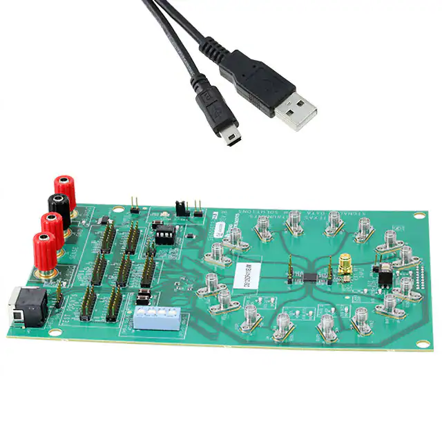


 工商网监
湘ICP备2023018690号
工商网监
湘ICP备2023018690号
