LM27222
LM27222 High-Speed 4.5A Synchronous MOSFET Driver
Literature Number: SNVS306A
�LM27222
High-Speed 4.5A Synchronous MOSFET Driver
General Description
Features
The LM27222 is a dual N-channel MOSFET driver designed
to drive MOSFETs in push-pull configurations as typically
used in synchronous buck regulators. The LM27222 takes
the PWM output from a controller and provides the proper
timing and drive levels to the power stage MOSFETs. Adaptive shoot-through protection prevents damaging and efficiency reducing shoot-through currents, thus ensuring a robust design capable of being used with nearly any MOSFET.
The adaptive shoot-through protection circuitry also reduces
the dead time down to as low as 10ns, ensuring the highest
operating efficiency. The peak sourcing and sinking current
for each driver of the LM27222 is about 3A and 4.5Amps
respectively with a Vgs of 5V. System performance is also
enhanced by keeping propagation delays down to 8ns. Efficiency is once again improved at all load currents by supporting synchronous, non-synchronous, and diode emulation
modes through the LEN pin. The minimum output pulse
width realized at the output of the MOSFETs is as low as
30ns. This enables high operating frequencies at very high
conversion ratios in buck regulator designs. To support low
power states in notebook systems, the LM27222 draws only
5µA from the 5V rail when the IN and LEN inputs are low or
floating.
n
n
n
n
n
n
n
n
n
n
n
Adaptive shoot-through protection
10ns dead time
8ns propagation delay
30ns minimum on-time
0.4Ω pull-down and 0.9Ω pull-up drivers
4.5A peak driving current
MOSFET tolerant design
5µA quiescent current
30V maximum input voltage in buck configuration
4V to 6.85V operating voltage
SO-8 and LLP packages
Applications
n
n
n
n
High Current Buck And Boost Voltage Converters
Fast Transient DC/DC Power Supplies
Single Ended Forward Output Rectification
CPU And GPU Core Voltage Regulators
Typical Application
20117902
FIGURE 1.
© 2006 National Semiconductor Corporation
DS201179
www.national.com
LM27222 High-Speed 4.5A Synchronous MOSFET Driver
March 2006
�LM27222
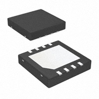
Connection Diagram
20117901
Top View
SO-8 (NS Package # M08A) θJA = 172˚C/W
or
LLP-8 (NS Package # SDC08A) θJA = 39˚C/W
Ordering Information
Order Number
Size
NSC Drawing #
LM27222M
SO-8
M08A
LM27222MX
LM27222SD
LLP-8
SDC08A
LM27222SDX
Package Type
Supplied As
Rail
95 Units/Rail
Tape and Reel
2500 Units/Reel
Tape and Reel
1000 Units/Reel
Tape and Reel
4500 Units/Reel
Pin Descriptions
Pin #
Pin Name
Pin Function
1
SW
High-side driver return. Should be connected to the common node of high and low-side MOSFETs.
2
HG
High-side gate drive output. Should be connected to the high-side MOSFET gate. Pulled down
internally to SW with a 10K resistor to prevent spurious turn on of the high-side MOSFET when the
driver is off.
3
CB
Bootstrap. Accepts a bootstrap voltage for powering the high-side driver.
4
IN
Accepts a PWM signal from a controller. Active High. Pulled down internally to GND with a 150K
resistor to prevent spurious turn on of the high-side MOSFET when the controller is inactive.
5
LEN
Low-side gate enable. Active High. Pulled down internally to GND with a 150K resistor to prevent
spurious turn-on of the low-side MOSFET when the controller is inactive.
6
VCC
Connect to +5V supply.
7
LG
Low-side gate drive output. Should be connected to low-side MOSFET gate. Pulled down internally to
GND with a 10K resistor to prevent spurious turn on of the low-side MOSFET when the driver is off.
8
GND
www.national.com
Ground.
2
�LM27222
Block Diagram
20117903
3
www.national.com
�LM27222
Absolute Maximum Ratings (Note 1)
Power Dissipation (Note 3)
If Military/Aerospace specified devices are required,
please contact the National Semiconductor Sales Office/
Distributors for availability and specifications.
Storage Temperature
VCC to GND
-0.3V to 7V
CB to GND
-0.3V to 36V
CB to SW
-0.3V to 7V
SW to GND (Note 2)
-2V to 36V
LEN, IN, LG to GND
-0.3V to VCC + 0.3V ≤ 7V
HG to GND
−65˚ to 150˚C
ESD Susceptibility
Human Body Model
2kV
Operating Ratings (Note 1)
VCC
4V to 6.85V
Junction Temperature Range
−40˚ to 125˚C
CB (max)
-0.3V to 36V
Junction Temperature
720mW
33V
+150˚C
Electrical Characteristics (Note 4)
VCC = CB = 5V, SW = GND = 0V, unless otherwise specified. Typicals and limits appearing in plain type apply for TA = TJ =
+25˚C. Limits appearing in boldface type apply over the entire operating temperature range (-40˚C ≤ TJ ≤ 125˚C).
Symbol
Parameter
Conditions
Min
Typ
Max
Units
5
15
µA
POWER SUPPLY
Iq_op
Operating Quiescent Current
IN = 0V, LEN = 0V
30
IN = 0V, LEN = 5V
500
540
650
µA
825
HIGH-SIDE DRIVER
Peak Pull-up Current
3
A
2.5
Ω
1.5
Ω
RH-pu
Pull-up Rds_on
RH-pd
Pull-down Rds_on
ISW = IHG = 0.3A
0.4
t4
Rise Time
Timing Diagram, CLOAD = 3.3nF
17
t6
Fall Time
Timing Diagram, CLOAD = 3.3nF
12
ns
t3
Pull-up Dead Time
Timing Diagram
9.5
ns
t5
Pull-down Delay
Timing Diagram
16.5
ns
30
ns
3.2
A
ICB = IHG = 0.3A
0.9
Peak Pull-down Current
ton_min
4.5
Minimum Positive Output
Pulse Width
A
ns
LOW-SIDE DRIVER
Peak Pull-up Current
RL-pu
Pull-up Rds_on
IVCC = ILG = 0.3A
0.9
Peak Pull-down Current
RL-pd
2.5
Ω
1.5
Ω
4.5
A
Pull-down Rds_on
IGND = ILG = 0.3A
0.4
t8
Rise Time
Timing Diagram, CLOAD = 3.3nF
17
t2
Fall Time
Timing Diagram, CLOAD = 3.3nF
14
ns
t7
Pull-up Dead Time
Timing Diagram
11.5
ns
t1
Pull-down Delay
Timing Diagram
7.7
ns
HG-SW Pull-down Resistance
10k
Ω
LG-GND Pull-down
Resistance
10k
Ω
LEN-GND Pull-down
Resistance
150K
Ω
IN-GND Pull-down Resistance
150K
Ω
IN = 0V, Source Current
50
nA
IN = 5V, Sink Current
33
µA
ns
PULL-DOWN RESISTANCES
LEAKAGE CURRENTS
Ileak_IN
IN pin Leakage Current
www.national.com
4
�(Continued)
VCC = CB = 5V, SW = GND = 0V, unless otherwise specified. Typicals and limits appearing in plain type apply for TA = TJ =
+25˚C. Limits appearing in boldface type apply over the entire operating temperature range (-40˚C ≤ TJ ≤ 125˚C).
Symbol
Ileak_LEN
Parameter
LEN pin Leakage Current
Conditions
Min
Typ
Max
Units
LEN = 0V, Source Current
200
nA
LEN = 5V, Sink Current
33
µA
LOGIC
VIH_LEN
LEN Low to High Threshold
VIL_LEN
Low to High Transition
LEN High to Low Threshold
High to Low Transition
VIH_IN
IN Low to High Threshold
Low to High Transition
VIL_IN
IN High to Low Threshold
High to Low Transition
Threshold Hysteresis
65
% of VCC
65
% of VCC
30
% of VCC
30
% of VCC
0.7
V
Note 1: Absolute Maximum Ratings are limits beyond which damage to the device may occur. Operating ratings are conditions under which the device operates
correctly. Operating Ratings do not imply guaranteed performance limits.
Note 2: The SW pin can have -2V to -0.5 volts applied for a maximum duty cycle of 10% with a maximum period of 1 second. There is no duty cycle or maximum
period limitation for a SW pin voltage range of -0.5V to 30 Volts.
Note 3: Maximum allowable power dissipation is a function of the maximum junction temperature, TJMAX, the junction-to-ambient thermal resistance, θJA, and the
ambient temperature, TA. The maximum allowable power dissipation at any ambient temperature is calculated using: PMAX = (TJMAX-TA) / θJA. The junction-toambient thermal resistance, θJA, for the LM27222M, it is 165˚C/W. For a TJMAX of 150˚C and TA of 25˚C, the maximum allowable power dissipation is 0.76W. The
θJA for the LM27222SD is 42˚C/W. For a TJMAX of 150˚C and TA of 25˚C, the maximum allowable power dissipation is 3W.
Note 4: Min and Max limits are 100% production tested at 25˚C. Limits over the operating temperature range are guaranteed through correlation using Statistical
Quality Control (SQC) methods. Limits are used to calculate National’s Average Outgoing Quality Level (AOQL).
Timing Diagram
20117904
5
www.national.com
LM27222
Electrical Characteristics (Note 4)
�LM27222
Typical Waveforms
20117908
20117907
FIGURE 3. PWM High-to-Low Transition at IN Input
FIGURE 2. PWM Low-to-High Transition at IN Input
20117909
FIGURE 4. LEN Operation
The typical waveforms are from a circuit similar to Figure 1 with:
Q1: 2 x Si7390DP
Q2: 2 x Si7356DP
L1: 0.4 µH
VIN: 12V
www.national.com
6
�LM27222
Application Information
GENERAL
The LM27222 is designed for high speed and high operating
reliability. The driver can handle very narrow, down to zero,
PWM pulses in a guaranteed, deterministic way. Therefore,
the HG and LG outputs are always in predictable states. No
latches are used in the HG and LG control logic so the
drivers cannot get "stuck" in the wrong state. The driver
design allows for powering up with a pre-biasing voltage
being present at the regulator output. To reduce conduction
losses in DC-DC converters with low duty factors the
LM27222 driver can be powered from a 6.5V ± 5% power
rail.
It is recommended to use the same power rail for both the
controller and driver. If two different power rails are used,
never allow the PWM pulse magnitude at the IN input or the
control voltage at the LEN input to be above the driver VCC
voltage or unpredictable HG and LG outputs pulse widths
may result.
20117906
MINIMUM PULSE WIDTH
As the input pulse width to the IN pin is decreased, the pulse
width of the high-side gate drive (HG-SW) also decreases.
However, for input pulse widths 60ns and smaller, the
HG-SW remains constant at 30ns. Thus the minimum pulse
width of the driver output is 30ns. Figure 5 shows an input
pulse at the IN pin 20ns wide, and the output of the driver, as
measured between the nodes HG and SW is a 30ns wide
pulse. Figure 6 shows the variation of the SW node pulse
width vs IN pulse width. At the IN pin, if a falling edge is
followed by a rising edge within 5ns, the HG may ignore the
rising edge and remain low until the IN pin toggles again. If a
rising edge is followed by a falling edge within 5ns, the pulse
may be completely ignored.
FIGURE 6.
ADAPTIVE SHOOT-THROUGH PROTECTION
The LM27222 prevents shoot-through power loss by ensuring that both the high- and low-side MOSFETs are not conducting at the same time. When the IN signal rises, LG is first
pulled down. The adaptive shoot-through protection circuit
waits for LG to reach 0.9V before turning on HG. Similarly,
when IN goes low, HG is pulled down first, and the circuit
turns LG on only after the voltage difference between the
high-side gate and the switch node, i.e. HG-SW, has fallen to
0.9V.
It is possible in some applications that at power-up the
driver’s SW pin is above 3V in either buck or boost comverter applications. For instance, in a buck configuration a
pre-biasing voltage can be either a voltage from anothert
power rail connected to the load, or a leakage voltage
through the load, or it can be an output capacitor precharged above 3V while no significant load is present. In a
boost application it can be an input voltage rail above 3V.
In the case of insufficient initial CB-SW voltage (less than
2V) such as when the output rail is pre-biased, the shootthrough protection circuit holds LG low for about 170ns,
beginning from the instant when IN goes high. After the
170ns delay, the status of LG is dictated by LEN and IN.
Once LG goes high and SW goes low, the bootstrap capacitor will be charged up (assuming SW is grounded for long
enough time). As a result, CB-SW will be close to 5V and the
LM27222 will now fully support synchronous operation.
The dead-time between the high- and low-side pulses is kept
as small as possible to minimize conduction through the
body diode of the low-side MOSFET(s).
20117905
FIGURE 5. Min On Time
7
www.national.com
�LM27222
Application Information
4.
The high-current loop between the high-side and lowside MOSFETs and the input capacitors should be as
small as possible.
5. There should be enough copper area near the MOSFETs and the inductor for heat dissipation. Vias may
also be added to carry the heat to other layers.
(Continued)
POWER DISSIPATION
The power dissipated in the driver IC when switching synchronously can be calculated as follows:
TYPICAL APPLICATION CIRCUIT DESCRIPITON
The Application Example on the following page shows the
LM27222 being used with National’s LM27212, a 2-phase
hysteretic current mode controller. Although this circuit is
capable of operating from 5V to 28V, the components are
optimized for an input voltage range of 9V to 28V. The
high-side FET is selected for low gate charge to reduce
switching losses. For low duty cycles, the average current
through the high-side FET is relatively small and thus we
trade off higher conduction losses for lower switching losses.
The low-side FET is selected solely on RDS_ON to minimize
conduction losses. If the input voltage range were 4V to 6V,
the MOSFET selection should be changed. First, much lower
voltage FETs can be used, and secondly, high-side FET
RDS_ON becomes a larger loss factor than the switching
losses. Of course with a lower input voltage, the input capacitor voltage rating can be reduced and the inductor value
can be reduced as well. For a 4V to 6V application, the
inductor can be reduced to 200nH to 300nH. The switching
frequency of the LM27212 is determined by the allowed
ripple current in the inductor. This circuit is set for approximately 300kHz. At lower input voltages, higher frequencies
are possible without suffering a significant efficiency loss.
Although the LM27222 can support operating frequencies up
to 2MHz in many applications, the LM27212 should be limited to about 1MHz. The control architecture of the LM27212
and the low propagation times of the LM27222 potentially
gives this solution the fastest transient response in the
industry.
where fSW = switching frequency
VCC = voltage at the VCC pin,
QG_H = total gate charge of the (parallel combination of the)
high-side MOSFET(s)
QG_L = total gate charge of the (parallel combination of the)
low-side MOSFET(s)
RG_H = gate resistance of the (parallel combination of the)
high-side MOSFET(s)
RG_L = gate resistance of the (parallel combination of the)
low-side MOSFET(S)
RH_pu = pull-up RDS_ON of the high-side driver
RH_pd = pull-down RDS_ON of the high-side driver
RL_pu = pull-up RDS_ON of the low-side driver
RL_pd = pull-down RDS_ON of the low-side driver
PC BOARD LAYOUT GUIDELINES
1. Place the driver as close to the MOSFETs as possible.
2. HG, SW, LG, GND: Run short, thick traces between the
driver and the MOSFETs. To minimize parasitics, the
traces for HG and SW should run parallel and close to
each other. The same is true for LG and GND.
3. Driver VCC: Place the decoupling capacitor close to the
VCC and GND pins.
www.national.com
8
�* Q1, Q3: 2 x Si7390DP
** Q2, Q4: 2 x Si7356DP
Application Example
20117920
LM27222
9
www.national.com
�LM27222
Physical Dimensions
inches (millimeters) unless otherwise noted
8-Lead Small Outline Package
Order Number: LM27222M, LM27222MX
NS Package Number M08A
8-Lead LLP Package
Order Number: LM27222SD, LM27222SDX
NS Package Number SDC08A
www.national.com
10
�LM27222 High-Speed 4.5A Synchronous MOSFET Driver
Notes
National does not assume any responsibility for use of any circuitry described, no circuit patent licenses are implied and National reserves
the right at any time without notice to change said circuitry and specifications.
For the most current product information visit us at www.national.com.
LIFE SUPPORT POLICY
NATIONAL’S PRODUCTS ARE NOT AUTHORIZED FOR USE AS CRITICAL COMPONENTS IN LIFE SUPPORT DEVICES OR SYSTEMS
WITHOUT THE EXPRESS WRITTEN APPROVAL OF THE PRESIDENT AND GENERAL COUNSEL OF NATIONAL SEMICONDUCTOR
CORPORATION. As used herein:
1. Life support devices or systems are devices or systems
which, (a) are intended for surgical implant into the body, or
(b) support or sustain life, and whose failure to perform when
properly used in accordance with instructions for use
provided in the labeling, can be reasonably expected to result
in a significant injury to the user.
2. A critical component is any component of a life support
device or system whose failure to perform can be reasonably
expected to cause the failure of the life support device or
system, or to affect its safety or effectiveness.
BANNED SUBSTANCE COMPLIANCE
National Semiconductor manufactures products and uses packing materials that meet the provisions of the Customer Products
Stewardship Specification (CSP-9-111C2) and the Banned Substances and Materials of Interest Specification (CSP-9-111S2) and contain
no ‘‘Banned Substances’’ as defined in CSP-9-111S2.
Leadfree products are RoHS compliant.
National Semiconductor
Americas Customer
Support Center
Email: new.feedback@nsc.com
Tel: 1-800-272-9959
www.national.com
National Semiconductor
Europe Customer Support Center
Fax: +49 (0) 180-530 85 86
Email: europe.support@nsc.com
Deutsch Tel: +49 (0) 69 9508 6208
English Tel: +44 (0) 870 24 0 2171
Français Tel: +33 (0) 1 41 91 8790
National Semiconductor
Asia Pacific Customer
Support Center
Email: ap.support@nsc.com
National Semiconductor
Japan Customer Support Center
Fax: 81-3-5639-7507
Email: jpn.feedback@nsc.com
Tel: 81-3-5639-7560
�IMPORTANT NOTICE
Texas Instruments Incorporated and its subsidiaries (TI) reserve the right to make corrections, modifications, enhancements, improvements,
and other changes to its products and services at any time and to discontinue any product or service without notice. Customers should
obtain the latest relevant information before placing orders and should verify that such information is current and complete. All products are
sold subject to TI’s terms and conditions of sale supplied at the time of order acknowledgment.
TI warrants performance of its hardware products to the specifications applicable at the time of sale in accordance with TI’s standard
warranty. Testing and other quality control techniques are used to the extent TI deems necessary to support this warranty. Except where
mandated by government requirements, testing of all parameters of each product is not necessarily performed.
TI assumes no liability for applications assistance or customer product design. Customers are responsible for their products and
applications using TI components. To minimize the risks associated with customer products and applications, customers should provide
adequate design and operating safeguards.
TI does not warrant or represent that any license, either express or implied, is granted under any TI patent right, copyright, mask work right,
or other TI intellectual property right relating to any combination, machine, or process in which TI products or services are used. Information
published by TI regarding third-party products or services does not constitute a license from TI to use such products or services or a
warranty or endorsement thereof. Use of such information may require a license from a third party under the patents or other intellectual
property of the third party, or a license from TI under the patents or other intellectual property of TI.
Reproduction of TI information in TI data books or data sheets is permissible only if reproduction is without alteration and is accompanied
by all associated warranties, conditions, limitations, and notices. Reproduction of this information with alteration is an unfair and deceptive
business practice. TI is not responsible or liable for such altered documentation. Information of third parties may be subject to additional
restrictions.
Resale of TI products or services with statements different from or beyond the parameters stated by TI for that product or service voids all
express and any implied warranties for the associated TI product or service and is an unfair and deceptive business practice. TI is not
responsible or liable for any such statements.
TI products are not authorized for use in safety-critical applications (such as life support) where a failure of the TI product would reasonably
be expected to cause severe personal injury or death, unless officers of the parties have executed an agreement specifically governing
such use. Buyers represent that they have all necessary expertise in the safety and regulatory ramifications of their applications, and
acknowledge and agree that they are solely responsible for all legal, regulatory and safety-related requirements concerning their products
and any use of TI products in such safety-critical applications, notwithstanding any applications-related information or support that may be
provided by TI. Further, Buyers must fully indemnify TI and its representatives against any damages arising out of the use of TI products in
such safety-critical applications.
TI products are neither designed nor intended for use in military/aerospace applications or environments unless the TI products are
specifically designated by TI as military-grade or "enhanced plastic." Only products designated by TI as military-grade meet military
specifications. Buyers acknowledge and agree that any such use of TI products which TI has not designated as military-grade is solely at
the Buyer's risk, and that they are solely responsible for compliance with all legal and regulatory requirements in connection with such use.
TI products are neither designed nor intended for use in automotive applications or environments unless the specific TI products are
designated by TI as compliant with ISO/TS 16949 requirements. Buyers acknowledge and agree that, if they use any non-designated
products in automotive applications, TI will not be responsible for any failure to meet such requirements.
Following are URLs where you can obtain information on other Texas Instruments products and application solutions:
Products
Applications
Audio
www.ti.com/audio
Communications and Telecom www.ti.com/communications
Amplifiers
amplifier.ti.com
Computers and Peripherals
www.ti.com/computers
Data Converters
dataconverter.ti.com
Consumer Electronics
www.ti.com/consumer-apps
DLP® Products
www.dlp.com
Energy and Lighting
www.ti.com/energy
DSP
dsp.ti.com
Industrial
www.ti.com/industrial
Clocks and Timers
www.ti.com/clocks
Medical
www.ti.com/medical
Interface
interface.ti.com
Security
www.ti.com/security
Logic
logic.ti.com
Space, Avionics and Defense
www.ti.com/space-avionics-defense
Power Mgmt
power.ti.com
Transportation and Automotive www.ti.com/automotive
Microcontrollers
microcontroller.ti.com
Video and Imaging
RFID
www.ti-rfid.com
OMAP Mobile Processors
www.ti.com/omap
Wireless Connectivity
www.ti.com/wirelessconnectivity
TI E2E Community Home Page
www.ti.com/video
e2e.ti.com
Mailing Address: Texas Instruments, Post Office Box 655303, Dallas, Texas 75265
Copyright © 2011, Texas Instruments Incorporated
�


 工商网监
湘ICP备2023018690号
工商网监
湘ICP备2023018690号
