Product
Folder
Sample &
Buy
Technical
Documents
Support &
Community
Tools &
Software
LM224K, LM224KA, LM324, LM324A, LM324K, LM324KA, LM2902
LM124, LM124A, LM224, LM224A, LM2902V, LM2902K, LM2902KV, LM2902KAV
SLOS066W – SEPTEMBER 1975 – REVISED MARCH 2015
LMx24, LMx24x, LMx24xx, LM2902, LM2902x, LM2902xx, LM2902xxx Quadruple
Operational Amplifiers
1 Features
2 Applications
•
•
•
•
•
•
•
•
1
•
•
•
•
•
•
•
•
2-kV ESD Protection for:
– LM224K, LM224KA
– LM324K, LM324KA
– LM2902K, LM2902KV, LM2902KAV
Wide Supply Ranges
– Single Supply: 3 V to 32 V
(26 V for LM2902)
– Dual Supplies: ±1.5 V to ±16 V
(±13 V for LM2902)
Low Supply-Current Drain Independent of
Supply Voltage: 0.8 mA Typical
Common-Mode Input Voltage Range Includes
Ground, Allowing Direct Sensing Near Ground
Low Input Bias and Offset Parameters
– Input Offset Voltage: 3 mV Typical
MM A Versions: 2 mV Typical
– Input Offset Current: 2 nA Typical
– Input Bias Current: 20 nA Typical
MMA Versions: 15 nA Typical
Differential Input Voltage Range Equal to
Maximum-Rated Supply Voltage:
32 V (26 V for LM2902)
Open-Loop Differential Voltage Amplification:
100 V/mV Typical
Internal Frequency Compensation
On Products Compliant to MIL-PRF-38535,
All Parameters are Tested Unless Otherwise
Noted. On All Other Products, Production
Processing Does Not Necessarily Include Testing
of All Parameters.
•
•
•
•
Blu-ray Players and Home Theaters
Chemical and Gas Sensors
DVD Recorders and Players
Digital Multimeter: Bench and Systems
Digital Multimeter: Handhelds
Field Transmitter: Temperature Sensors
Motor Control: AC Induction, Brushed DC,
Brushless DC, High-Voltage, Low-Voltage,
Permanent Magnet, and Stepper Motor
Oscilloscopes
TV: LCD and Digital
Temperature Sensors or Controllers Using
Modbus
Weigh Scales
3 Description
These devices consist of four independent high-gain
frequency-compensated operational amplifiers that
are designed specifically to operate from a single
supply or split supply over a wide range of voltages.
Device Information(1)
PART NUMBER
LMx24, LMx24x,
LMx24xx, LM2902,
LM2902x,
LM2902xx,
LM2902xxx
LM124, LM124A
PACKAGE
BODY SIZE (NOM)
SOIC (14)
8.65 mm × 3.91 mm
CDIP (14)
19.56 mm × 6.67 mm
PDIP (14)
19.30 mm × 6.35 mm
CFP (14)
9.21 mm × 5.97 mm
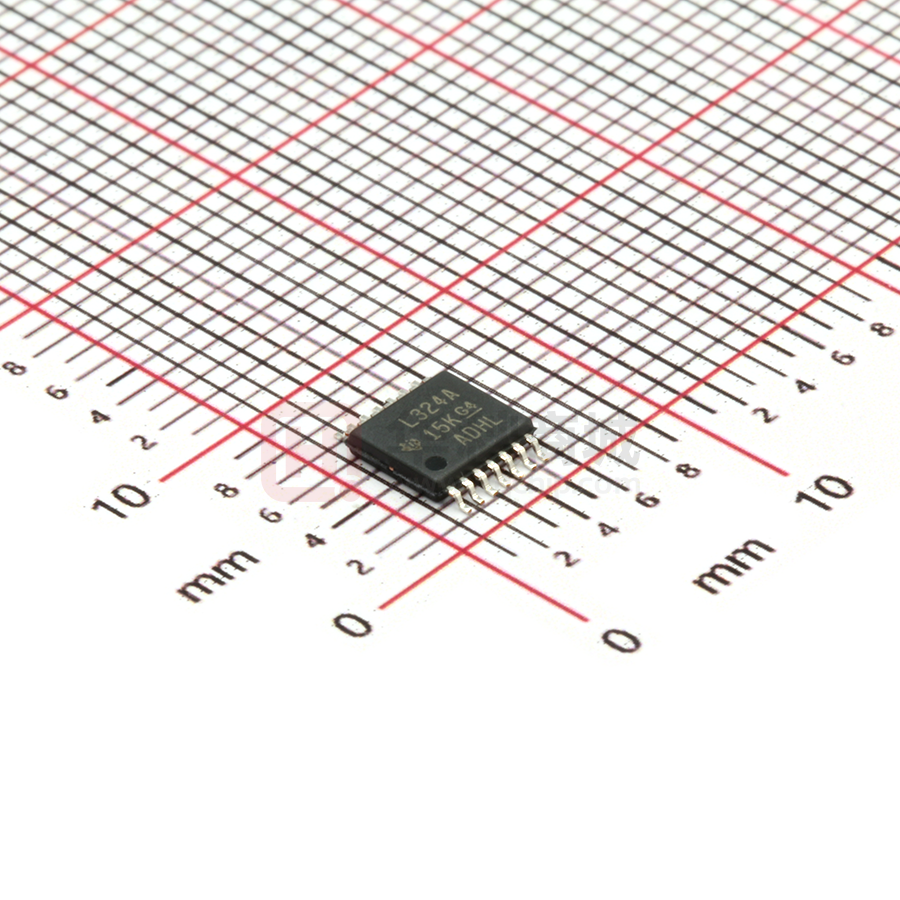
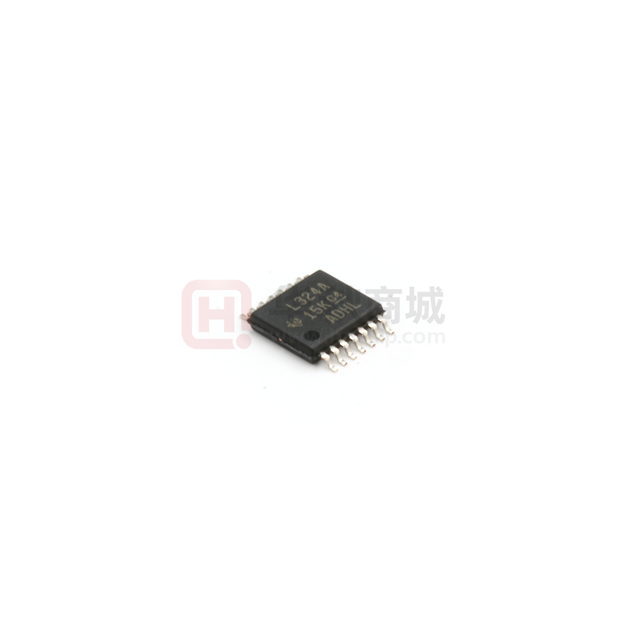
TSSOP (14)
5.00 mm × 4.40 mm
SO (14)
9.20 mm × 5.30 mm
SSOP (14)
6.20 mm × 5.30 mm
LCCC (20)
8.90 mm × 8.90 mm
(1) For all available packages, see the orderable addendum at
the end of the data sheet.
Symbol (Each Amplifier)
−
IN−
OUT
+
IN+
1
An IMPORTANT NOTICE at the end of this data sheet addresses availability, warranty, changes, use in safety-critical applications,
intellectual property matters and other important disclaimers. PRODUCTION DATA.
�LM224K, LM224KA, LM324, LM324A, LM324K, LM324KA, LM2902
LM124, LM124A, LM224, LM224A, LM2902V, LM2902K, LM2902KV, LM2902KAV
SLOS066W – SEPTEMBER 1975 – REVISED MARCH 2015
www.ti.com
Table of Contents
1
2
3
4
5
6
Features ..................................................................
Applications ...........................................................
Description .............................................................
Revision History.....................................................
Pin Configuration and Functions .........................
Specifications.........................................................
1
1
1
2
3
4
6.1
6.2
6.3
6.4
6.5
6.6
6.7
4
4
4
5
5
6
Absolute Maximum Ratings ......................................
ESD Ratings ............................................................
Recommended Operating Conditions.......................
Thermal Information ..................................................
Electrical Characteristics for LMx24 and LM324K ....
Electrical Characteristics for LM2902 and LM2902V
Electrical Characteristics for LMx24A and
LM324KA ...................................................................
6.8 Operating Conditions ................................................
6.9 Typical Characteristics ..............................................
7
8
6
7
8
Parameter Measurement Information .................. 9
Detailed Description ............................................ 10
8.1
8.2
8.3
8.4
9
Overview .................................................................
Functional Block Diagram .......................................
Feature Description.................................................
Device Functional Modes........................................
10
10
11
11
Application and Implementation ........................ 12
9.1 Application Information............................................ 12
9.2 Typical Application ................................................. 12
10 Power Supply Recommendations ..................... 13
11 Layout................................................................... 13
11.1 Layout Guidelines ................................................. 13
11.2 Layout Examples................................................... 14
12 Device and Documentation Support ................. 15
12.1
12.2
12.3
12.4
12.5
Documentation Support .......................................
Related Links ........................................................
Trademarks ...........................................................
Electrostatic Discharge Caution ............................
Glossary ................................................................
15
15
15
15
15
13 Mechanical, Packaging, and Orderable
Information ........................................................... 15
4 Revision History
NOTE: Page numbers for previous revisions may differ from page numbers in the current version.
Changes from Revision V (January 2014) to Revision W
Page
•
Added Applications ................................................................................................................................................................. 1
•
Added Device Information table ............................................................................................................................................. 1
•
Added Device and Documentation Support section............................................................................................................. 15
•
Added Mechanical, Packaging, and Orderable Information section..................................................................................... 15
Changes from Revision U (August 2010) to Revision V
Page
•
Updated document to new TI data sheet format - no specification changes. ........................................................................ 1
•
Updated Features ................................................................................................................................................................... 1
•
Removed Ordering Information table ..................................................................................................................................... 3
•
Added ESD warning. ............................................................................................................................................................ 15
2
Submit Documentation Feedback
Copyright © 1975–2015, Texas Instruments Incorporated
Product Folder Links: LM224K LM224KA LM324 LM324A LM324K LM324KA LM2902 LM124 LM124A LM224
LM224A LM2902V LM2902K LM2902KV LM2902KAV
�LM224K, LM224KA, LM324, LM324A, LM324K, LM324KA, LM2902
LM124, LM124A, LM224, LM224A, LM2902V, LM2902K, LM2902KV, LM2902KAV
www.ti.com
SLOS066W – SEPTEMBER 1975 – REVISED MARCH 2015
5 Pin Configuration and Functions
FK Package
20-Pin LCCC
(Top View)
1IN−
1OUT
NC
4OUT
4IN−
D, DB, J, N, NS, PW, W
14-Pin SOIC, SSOP, CDIP, PDIP, SO, TSSOP, CFP
(Top View)
1IN+
NC
VCC
NC
2IN+
4
3 2 1 20 19
18
17
5
6
16
7
15
14
9 10 11 12 13
4IN+
NC
GND
NC
3IN+
1
14
2
13
3
12
4
11
5
10
6
9
7
8
4OUT
4IN−
4IN+
GND
3IN+
3IN−
3OUT
2IN−
2OUT
NC
3OUT
3IN−
8
1OUT
1IN−
1IN+
VCC
2IN+
2IN−
2OUT
Pin Functions
PIN
LCCC NO.
SOIC, SSOP,
CDIP, PDIP,
SO, TSSOP,
CFP NO.
1IN–
3
2
I
Negative input
1IN+
4
3
I
Positive input
1OUT
2
1
O
Output
2IN–
9
6
I
Negative input
2IN+
8
5
I
Positive input
2OUT
10
7
O
Output
3IN–
13
9
I
Negative input
3IN+
14
10
I
Positive input
3OUT
12
8
O
Output
4IN–
19
13
I
Negative input
4IN+
18
12
I
Positive input
4OUT
20
14
O
Output
GND
16
11
—
Ground
—
—
Do not connect
4
—
Power supply
NAME
I/O
DESCRIPTION
1
5
NC
7
11
15
17
VCC
6
Copyright © 1975–2015, Texas Instruments Incorporated
Submit Documentation Feedback
Product Folder Links: LM224K LM224KA LM324 LM324A LM324K LM324KA LM2902 LM124 LM124A LM224
LM224A LM2902V LM2902K LM2902KV LM2902KAV
3
�LM224K, LM224KA, LM324, LM324A, LM324K, LM324KA, LM2902
LM124, LM124A, LM224, LM224A, LM2902V, LM2902K, LM2902KV, LM2902KAV
SLOS066W – SEPTEMBER 1975 – REVISED MARCH 2015
www.ti.com
6 Specifications
6.1 Absolute Maximum Ratings
over operating free-air temperature range (unless otherwise noted) (1)
LMx24, LMx24x,
LMx24xx, LM2902x,
LM2902xx, LM2902xxx
LM2902
Supply voltage, VCC (2)
Differential input voltage, VID
MIN
MAX
MIN
MAX
±13
26
±16
32
V
±32
V
–0.3
to 32
V
(3)
±26
Input voltage, VI (either input)
–0.3
Duration of output short circuit (one amplifier) to ground at (or
below) TA = 25°C, VCC ≤ 15 V (4)
26
Unlimited
Operating virtual junction temperature, TJ
FK package
Lead temperature 1.6 mm (1/16 inch)
from case for 60 seconds
J or W package
300
Storage temperature, Tstg
(1)
(2)
(3)
(4)
Unlimited
150
Case temperature for 60 seconds
UNIT
–65
150
–65
150
°C
260
°C
300
°C
150
°C
Stresses beyond those listed under Absolute Maximum Ratings may cause permanent damage to the device. These are stress ratings
only, and functional operation of the device at these or any other conditions beyond those indicated under Recommended Operating
Conditions is not implied. Exposure to absolute-maximum-rated conditions for extended periods may affect device reliability.
All voltage values (except differential voltages and VCC specified for the measurement of IOS) are with respect to the network GND.
Differential voltages are at IN+, with respect to IN−.
Short circuits from outputs to VCC can cause excessive heating and eventual destruction.
6.2 ESD Ratings
VALUE
UNIT
LM224K, LM224KA, LM324K, LM324KA, LM2902K, LM2902KV, LM2902KAV
V(ESD)
Electrostatic discharge
Human-body model (HBM), per ANSI/ESDA/JEDEC JS-001 (1)
±2000
Charged-device model (CDM), per JEDEC specification JESD22-C101
±1000
V
LM124, LM124A, LM224, LM224A, LM324, LM324A, LM2902, LM2902V
V(ESD)
(1)
Electrostatic discharge
Human-body model (HBM), per ANSI/ESDA/JEDEC JS-001 (1)
±500
Charged-device model (CDM), per JEDEC specification JESD22-C101
±1000
V
JEDEC document JEP155 states that 500-V HBM allows safe manufacturing with a standard ESD control process.
6.3 Recommended Operating Conditions
over operating free-air temperature range (unless otherwise noted)
LMx24, LMx24x, LMx24xx,
LM2902x, LM2902xx, LM2902xxx
LM2902
MIN
MAX
MIN
UNIT
MAX
VCC Supply voltage
3
26
3
30
V
VCM Common-mode voltage
0
VCC – 2
0
VCC – 2
V
–55
125
LM324
0
70
LM224
–25
85
LM124
TA Operating free air
temperature
4
LM2904
Submit Documentation Feedback
–40
125
°C
Copyright © 1975–2015, Texas Instruments Incorporated
Product Folder Links: LM224K LM224KA LM324 LM324A LM324K LM324KA LM2902 LM124 LM124A LM224
LM224A LM2902V LM2902K LM2902KV LM2902KAV
�LM224K, LM224KA, LM324, LM324A, LM324K, LM324KA, LM2902
LM124, LM124A, LM224, LM224A, LM2902V, LM2902K, LM2902KV, LM2902KAV
www.ti.com
SLOS066W – SEPTEMBER 1975 – REVISED MARCH 2015
6.4 Thermal Information
LMx24, LM2902
DB
(SSOP)
N (PDIP)
NS (SO)
PW
(TSSOP)
FK
(LCCC)
J (CDIP)
W (CFP)
14 PINS
14 PINS
14 PINS
14 PINS
14 PINS
20 PINS
14 PINS
14 PINS
Junction-toambient thermal
resistance
86
86
80
76
113
—
—
—
Junction-to-case
(top) thermal
resistance
—
THERMAL METRIC
RθJA
(2) (3)
RθJC (4)
(1)
(2)
(3)
(4)
LMx24
D (SOIC)
(1)
UNIT
°C/W
—
—
—
—
5.61
15.05
14.65
For more information about traditional and new thermal metrics, see the IC Package Thermal Metrics application report, SPRA953.
Short circuits from outputs to VCC can cause excessive heating and eventual destruction.
Maximum power dissipation is a function of TJ(max), RθJA, and TA. The maximum allowable power dissipation at any allowable ambient
temperature is PD = (TJ(max) – TA)/RθJA. Operating at the absolute maximum TJ of 150°C can affect reliability.
Maximum power dissipation is a function of TJ(max), RθJA, and TC. The maximum allowable power dissipation at any allowable case
temperature is PD = (TJ(max) – TC)/RθJC. Operating at the absolute maximum TJ of 150°C can affect reliability.
6.5 Electrical Characteristics for LMx24 and LM324K
at specified free-air temperature, VCC = 5 V (unless otherwise noted)
PARAMETER
VIO
Input offset voltage
IIO
Input offset current
IIB
Input bias current
VICR
Common-mode input voltage range
TEST CONDITIONS (1)
VCC = 5 V to MAX, VIC = VICRmin,
VO = 1.4 V
TA (2)
LM124, LM224
MIN
25°C
2
VCC = 5 V to MAX
RL = 2 kΩ
25°C
RL = 10 kΩ
25°C
–20
–250
–500
0 to
VCC – 2
VCC – 1.5
VCC – 1.5
26
27
Common-mode rejection ratio
VIC = VICRmin
kSVR
Supply-voltage rejection ratio
(ΔVCC /ΔVIO)
VO1/ VO2
Crosstalk attenuation
(2)
(3)
–150
0 to
VCC – 2
Full range
CMRR
(1)
50
150
0 to
VCC – 1.5
RL ≥ 10 kΩ
AVD
Supply current (four amplifiers)
2
V
V
VCC = 15 V, VO = 1 V to 11 V,
RL ≥ 2 kΩ
ICC
30
0 to
VCC – 1.5
26
Large-signal differential voltage
amplification
Short-circuit output current
9
–300
Full range
RL ≤ 10 kΩ
IOS
–20
RL = 2 kΩ
Low-level output voltage
Full range
28
5
27
28
25
100
20
100
5
20
mV
25°C
50
Full range
25
25°C
70
80
65
80
dB
25°C
65
100
65
100
dB
V/mV
f = 1 kHz to 20 kHz
25°C
VCC = 15 V,
VID = 1 V,
VO = 0
25°C
–20
Full range
–10
25°C
10
VCC = 15 V,
VID = –1 V,
VO = 15 V
7
nA
VOL
Output current
3
100
Full range
Full range
IO
MAX
nA
Full range
VO = 1.4 V
VCC = MAX
5
UNIT
TYP (3)
mV
25°C
High-level output voltage
3
MIN
7
25°C
VOH
MAX
Full range
25°C
VO = 1.4 V
LM324, LM324K
TYP (3)
15
120
–30
120
–60
–20
–30
dB
–60
Source
–10
mA
20
10
30
12
20
Sink
Full range
5
VID = –1 V, VO = 200 mV
25°C
12
5
VCC at 5 V, VO = 0,
GND at –5 V
25°C
±40
±60
±40
±60
VO = 2.5 V, no load
Full range
0.7
1.2
0.7
1.2
VCC = MAX, VO = 0.5 VCC,
no load
Full range
1.4
3
1.4
3
μA
30
mA
mA
All characteristics are measured under open-loop conditions, with zero common-mode input voltage, unless otherwise specified. MAX
VCC for testing purposes is 26 V for LM2902 and 30 V for the others.
Full range is –55°C to 125°C for LM124, –25°C to 85°C for LM224, and 0°C to 70°C for LM324.
All typical values are at TA = 25°C
Copyright © 1975–2015, Texas Instruments Incorporated
Submit Documentation Feedback
Product Folder Links: LM224K LM224KA LM324 LM324A LM324K LM324KA LM2902 LM124 LM124A LM224
LM224A LM2902V LM2902K LM2902KV LM2902KAV
5
�LM224K, LM224KA, LM324, LM324A, LM324K, LM324KA, LM2902
LM124, LM124A, LM224, LM224A, LM2902V, LM2902K, LM2902KV, LM2902KAV
SLOS066W – SEPTEMBER 1975 – REVISED MARCH 2015
www.ti.com
6.6 Electrical Characteristics for LM2902 and LM2902V
at specified free-air temperature, VCC = 5 V (unless otherwise noted)
TEST CONDITIONS (1)
PARAMETER
VIO
VCC = 5 V to MAX,
VIC = VICRmin,
VO = 1.4 V
Input offset voltage
ΔVIO/ΔT
Input offset voltage temperature drift
LM2902
TA (2)
Non-A-suffix
devices
MIN
25°C
Input offset current
ΔIIO/ΔT
Input offset voltage temperature drift
3
1
4
2
VCC = 5 V to MAX
10
25°C
Large-signal differential voltage
amplification
CMRR
Common-mode rejection ratio
VIC = VICRmin
kSVR
Supply-voltage rejection ratio
(ΔVCC /ΔVIO)
VO1/ VO2
Crosstalk attenuation
Supply current (four amplifiers)
(1)
(2)
(3)
–250
pA/°C
–20
–250
–500
–500
0 to
VCC – 1.5
0 to
VCC – 1.5
0 to
VCC – 2
0 to
VCC – 2
VCC – 1.5
VCC – 1.5
RL = 2 kΩ
Full range
22
26
RL ≥ 10 kΩ
Full range
23
24
Full range
V
V
27
5
20
5
100
25
20
mV
25°C
25
Full range
15
100
25°C
50
80
60
80
dB
25°C
50
100
60
100
dB
V/mV
f = 1 kHz to 20 kHz
25°C
VCC = 15 V,
VID = 1 V,
VO = 0
25°C
–20
Full range
–10
25°C
10
Full range
5
15
120
120
–30
–60
–20
dB
–30
–60
Source
–10
mA
VCC = 15 V,
VID = –1 V,
VO = 15 V
ICC
–20
25°C
RL = 10 kΩ
AVD
Short-circuit output current
150
nA
VCC = 15 V,
VO = 1 V to 11 V,
RL ≥ 2 kΩ
IOS
50
300
Full range
RL ≤ 10 kΩ
Output current
μV/°C
2
Ful range
Low-level output voltage
IO
50
nA
VCC = MAX
VOL
2
7
Full range
RL = 2 kΩ
High-level output voltage
7
10
Ful range
Full range
VOH
3
Full range
RS = 0 Ω
VO = 1.4 V
Common-mode input voltage range
7
MAX
mV
25°C
VICR
UNIT
TYP (3)
25°C
A-suffix
devices
VO = 1.4 V
Input bias current
MIN
10
25°C
IIB
MAX
Full range
25°C
IIO
LM2902V
TYP (3)
20
10
12
20
Sink
5
μA
VID = –1 V, VO = 200 mV
25°C
30
VCC at 5 V, VO = 0, GND at –5 V
25°C
±40
±60
±40
40
±60
VO = 2.5 V, no load
Full range
0.7
1.2
0.7
1.2
VCC = MAX, VO = 0.5 VCC,
no load
Full range
1.4
3
1.4
3
mA
mA
All characteristics are measured under open-loop conditions, with zero common-mode input voltage, unless otherwise specified. MAX
VCC for testing purposes is 26 V for LM2902 and 32 V for LM2902V.
Full range is –40°C to 125°C for LM2902.
All typical values are at TA = 25°C.
6.7 Electrical Characteristics for LMx24A and LM324KA
at specified free-air temperature, VCC = 5 V (unless otherwise noted)
PARAMETER
TEST CONDITIONS (1)
VIO
Input offset
voltage
VCC = 5 V to 30 V,
VIC = VICRmin,
VO = 1.4 V
IIO
Input offset
current
VO = 1.4 V
IIB
Input bias
current
VO = 1.4 V
(1)
(2)
(3)
6
TA (2)
LM124A
MIN
TYP (3)
LM224A
MAX
25°C
2
Full range
4
25°C
10
Full range
30
MIN
LM324A, LM324KA
TYP (3)
MAX
2
3
MIN
UNIT
TYP (3)
MAX
2
3
mV
4
2
15
5
2
30
nA
25°C
–50
Full range
–100
30
–15
–80
75
–15
–100
nA
–100
–200
All characteristics are measured under open-loop conditions, with zero common-mode input voltage, unless otherwise specified.
Full range is –55°C to 125°C for LM124A, –25°C to 85°C for LM224A, and 0°C to 70°C for LM324A.
All typical values are at TA = 25°C.
Submit Documentation Feedback
Copyright © 1975–2015, Texas Instruments Incorporated
Product Folder Links: LM224K LM224KA LM324 LM324A LM324K LM324KA LM2902 LM124 LM124A LM224
LM224A LM2902V LM2902K LM2902KV LM2902KAV
�LM224K, LM224KA, LM324, LM324A, LM324K, LM324KA, LM2902
LM124, LM124A, LM224, LM224A, LM2902V, LM2902K, LM2902KV, LM2902KAV
www.ti.com
SLOS066W – SEPTEMBER 1975 – REVISED MARCH 2015
Electrical Characteristics for LMx24A and LM324KA (continued)
at specified free-air temperature, VCC = 5 V (unless otherwise noted)
TEST CONDITIONS (1)
PARAMETER
VICR
Common-mode
input voltage
range
25°C
VCC = 30 V
Full range
High-level
output voltage
VCC = 30 V
kSVR
Supply-voltage
rejection ratio
(ΔVCC /ΔVIO)
VO1/ VO2
Crosstalk
attenuation
ICC
Supply current
(four amplifiers)
0 to
VCC – 2
VCC – 1.5
27
VIC = VICRmin
IOS
0 to
VCC – 2
27
Common-mode
rejection ratio
Short-circuit
output current
0 to
VCC − 2
Full range
CMRR
MIN
0 to
VCC – 1.5
RL≥ 10 kΩ
VCC = 15 V,
VO = 1 V to 11 V,
RL ≥ 2 kΩ
LM324A, LM324KA
MAX
0 to
VCC – 1.5
26
Large-signal
differential
voltage
amplification
TYP (3)
0 to
VCC − 1.5
VCC – 1.5
AVD
Full range
20
50
UNIT
MAX
V
26
28
5
100
TYP (3)
V
27
28
20
100
5
25
20
mV
25°C
50
100
Full range
25
25
25°C
70
70
80
65
80
dB
25°C
65
65
100
65
100
dB
120
dB
V/mV
f = 1 kHz to 20 kHz
VCC = 15 V,
VID = –1 V,
VO = 15 V
MIN
26
RL ≤ 10 kΩ
Output current
LM224A
MAX
VCC − 1.5
25°C
Low-level output
voltage
IO
TYP (3)
Full range
VOL
VCC = 15 V,
VID = 1 V,
VO = 0
LM124A
MIN
RL= 2 kΩ
RL = 2 kΩ
VOH
TA (2)
25°C
120
15
120
25°C
–20
–20
Full range
–10
–10
25°C
10
10
–30
–60
–20
–30
–60
Source
–10
mA
20
1
30
12
20
Sink
Full range
5
5
VID = −1 V, VO = 200 mV
25°C
12
12
5
VCC at 5 V, GND at –5 V,
VO = 0
25°C
±40
±60
±40
±60
±40
±60
VO = 2.5 V, no load
Full range
0.7
1.2
0.7
1.2
0.7
1.2
VCC = 30 V, VO = 15 V,
no load
Full range
1.4
3.
1.4
3
1.4
3
μA
30
mA
mA
6.8 Operating Conditions
VCC = ±15 V, TA = 25°C
PARAMETER
TEST CONDITIONS
TYP
UNIT
SR
Slew rate at unity gain
RL = 1 MΩ, CL = 30 pF, VI = ±10 V (see Figure 7)
0.5
V/μs
B1
Unity-gain bandwidth
RL = 1 MΩ, CL = 20 pF (see Figure 7)
1.2
MHz
Vn
Equivalent input noise voltage
RS = 100 Ω, VI = 0 V, f = 1 kHz (see Figure 8)
35
nV/√Hz
Copyright © 1975–2015, Texas Instruments Incorporated
Submit Documentation Feedback
Product Folder Links: LM224K LM224KA LM324 LM324A LM324K LM324KA LM2902 LM124 LM124A LM224
LM224A LM2902V LM2902K LM2902KV LM2902KAV
7
�LM224K, LM224KA, LM324, LM324A, LM324K, LM324KA, LM2902
LM124, LM124A, LM224, LM224A, LM2902V, LM2902K, LM2902KV, LM2902KAV
SLOS066W – SEPTEMBER 1975 – REVISED MARCH 2015
www.ti.com
6.9 Typical Characteristics
10
Output Voltage Referenced to +Vcc (V)
8
Output Voltage (V)
5
3
2
1
0.5
0.3
0.2
0.1
0.05
0.03
0.02
VCC = 15 V
VCC = 5 V
VCC = 30 V
0.01
0.001
0.01
0.1 0.2 0.5 1 2 3 5 710 20
Output Sink Current (mA)
VCC = 15 V
7
6
5
4
3
2
1
0.001
50 100
0.01
D001
Figure 1. Output Sinking Characteristics
0.1 0.2 0.5 1 2 3 5 710 20
Output Source Current (mA)
50 100
D002
Figure 2. Output Sourcing Characteristics
0.09
3.25
3
0.08
2.75
0.07
Output Voltage (V)
2.5
Iout (A)
0.06
0.05
0.04
0.03
2.25
2
1.75
1.5
1.25
1
0.02
Input
Output
0.75
0.01
0.5
0
-55 -40 -25 -10
0.25
5
20 35 50 65
Temperature (qC)
80
0
95 110 125
10
15
20
25
30
Time (PS)
35
40
45
50
D004
Figure 4. Voltage Follower Large Signal Response (50 pF)
90
20
80
17.5
70
Output Swing (Vpp)
Common-Mode Rejection Ratio (dB)
Figure 3. Source Current Limiting
60
50
40
30
15
12.5
10
7.5
5
20
2.5
10
0
100 200
500 1000
10000
Frequency (Hz)
100000
Figure 5. Common-Mode Rejection Ratio
8
5
D003
Submit Documentation Feedback
1000000
D006
0
1000 2000
5000 10000
100000
Frequency (Hz)
1000000
D007
Figure 6. Maximum Output Swing vs. Frequency
(VCC = 15 V)
Copyright © 1975–2015, Texas Instruments Incorporated
Product Folder Links: LM224K LM224KA LM324 LM324A LM324K LM324KA LM2902 LM124 LM124A LM224
LM224A LM2902V LM2902K LM2902KV LM2902KAV
�LM224K, LM224KA, LM324, LM324A, LM324K, LM324KA, LM2902
LM124, LM124A, LM224, LM224A, LM2902V, LM2902K, LM2902KV, LM2902KAV
www.ti.com
SLOS066W – SEPTEMBER 1975 – REVISED MARCH 2015
7 Parameter Measurement Information
900 Ω
VCC+
VCC+
−
VI
VO
+
100 Ω
−
VI = 0 V
RS
VCC−
CL
RL
VO
+
VCC−
Figure 7. Unity-Gain Amplifier
Copyright © 1975–2015, Texas Instruments Incorporated
Figure 8. Noise-Test Circuit
Submit Documentation Feedback
Product Folder Links: LM224K LM224KA LM324 LM324A LM324K LM324KA LM2902 LM124 LM124A LM224
LM224A LM2902V LM2902K LM2902KV LM2902KAV
9
�LM224K, LM224KA, LM324, LM324A, LM324K, LM324KA, LM2902
LM124, LM124A, LM224, LM224A, LM2902V, LM2902K, LM2902KV, LM2902KAV
SLOS066W – SEPTEMBER 1975 – REVISED MARCH 2015
www.ti.com
8 Detailed Description
8.1 Overview
These devices consist of four independent high-gain frequency-compensated operational amplifiers that are
designed specifically to operate from a single supply over a wide range of voltages. Operation from split supplies
also is possible if the difference between the two supplies is 3 V to 32 V (3 V to 26 V for the LM2902 device),
and VCC is at least 1.5 V more positive than the input common-mode voltage. The low supply-current drain is
independent of the magnitude of the supply voltage.
Applications include transducer amplifiers, DC amplification blocks, and all the conventional operational-amplifier
circuits that now can be more easily implemented in single-supply-voltage systems. For example, the LM124
device can be operated directly from the standard 5-V supply that is used in digital systems and provides the
required interface electronics, without requiring additional ±15-V supplies.
8.2 Functional Block Diagram
VCC
≈6-µA
Current
Regulator
≈6-µA
Current
Regulator
≈100-µA
Current
Regulator
OUT
IN−
†
≈50-µA
Current
Regulator
IN+
†
GND
To Other
Amplifiers
COMPONENT COUNT
(total device)
Epi-FET
Transistors
Diodes
Resistors
Capacitors
†
10
1
95
4
11
4
ESD protection cells - available on LM324K and LM324KA only
Submit Documentation Feedback
Copyright © 1975–2015, Texas Instruments Incorporated
Product Folder Links: LM224K LM224KA LM324 LM324A LM324K LM324KA LM2902 LM124 LM124A LM224
LM224A LM2902V LM2902K LM2902KV LM2902KAV
�LM224K, LM224KA, LM324, LM324A, LM324K, LM324KA, LM2902
LM124, LM124A, LM224, LM224A, LM2902V, LM2902K, LM2902KV, LM2902KAV
www.ti.com
SLOS066W – SEPTEMBER 1975 – REVISED MARCH 2015
8.3 Feature Description
8.3.1 Unity-Gain Bandwidth
Gain bandwidth product is found by multiplying the measured bandwidth of an amplifier by the gain at which that
bandwidth was measured. These devices have a high gain bandwidth of 1.2 MHz.
8.3.2 Slew Rate
The slew rate is the rate at which an operational amplifier can change its output when there is a change on the
input. These devices have a 0.5-V/μs slew rate.
8.3.3 Input Common Mode Range
The valid common mode range is from device ground to VCC – 1.5 V (VCC – 2 V across temperature). Inputs may
exceed VCC up to the maximum VCC without device damage. At least one input must be in the valid input
common mode range for output to be correct phase. If both inputs exceed valid range then output phase is
undefined. If either input is less than –0.3 V then input current should be limited to 1 mA and output phase is
undefined.
8.4 Device Functional Modes
These devices are powered on when the supply is connected. This device can be operated as a single supply
operational amplifier or dual supply amplifier depending on the application.
Copyright © 1975–2015, Texas Instruments Incorporated
Submit Documentation Feedback
Product Folder Links: LM224K LM224KA LM324 LM324A LM324K LM324KA LM2902 LM124 LM124A LM224
LM224A LM2902V LM2902K LM2902KV LM2902KAV
11
�LM224K, LM224KA, LM324, LM324A, LM324K, LM324KA, LM2902
LM124, LM124A, LM224, LM224A, LM2902V, LM2902K, LM2902KV, LM2902KAV
SLOS066W – SEPTEMBER 1975 – REVISED MARCH 2015
www.ti.com
9 Application and Implementation
NOTE
Information in the following applications sections is not part of the TI component
specification, and TI does not warrant its accuracy or completeness. TI’s customers are
responsible for determining suitability of components for their purposes. Customers should
validate and test their design implementation to confirm system functionality.
9.1 Application Information
The LMx24 and LM2902 operational amplifiers are useful in a wide range of signal conditioning applications.
Inputs can be powered before VCC for flexibility in multiple supply circuits.
9.2 Typical Application
A typical application for an operational amplifier in an inverting amplifier. This amplifier takes a positive voltage
on the input, and makes it a negative voltage of the same magnitude. In the same manner, it also makes
negative voltages positive.
RF
RI
Vsup+
VOUT
VIN
+
Vsup-
Figure 9. Application Schematic
9.2.1 Design Requirements
The supply voltage must be chosen such that it is larger than the input voltage range and output range. For
instance, this application will scale a signal of ±0.5 V to ±1.8 V. Setting the supply at ±12 V is sufficient to
accommodate this application.
9.2.2 Detailed Design Procedure
Determine the gain required by the inverting amplifier using Equation 1 and Equation 2:
(1)
(2)
Once the desired gain is determined, choose a value for RI or RF. Choosing a value in the kilohm range is
desirable because the amplifier circuit will use currents in the milliamp range. This ensures the part will not draw
too much current. This example will choose 10 kΩ for RI which means 36 kΩ will be used for RF. This was
determined by Equation 3.
(3)
12
Submit Documentation Feedback
Copyright © 1975–2015, Texas Instruments Incorporated
Product Folder Links: LM224K LM224KA LM324 LM324A LM324K LM324KA LM2902 LM124 LM124A LM224
LM224A LM2902V LM2902K LM2902KV LM2902KAV
�LM224K, LM224KA, LM324, LM324A, LM324K, LM324KA, LM2902
LM124, LM124A, LM224, LM224A, LM2902V, LM2902K, LM2902KV, LM2902KAV
www.ti.com
SLOS066W – SEPTEMBER 1975 – REVISED MARCH 2015
Typical Application (continued)
9.2.3 Application Curve
2
VIN
1.5
VOUT
1
Volts
0.5
0
-0.5
-1
-1.5
-2
0
0.5
1
Time (ms)
1.5
2
Figure 10. Input and Output Voltages of the Inverting Amplifier
10 Power Supply Recommendations
CAUTION
Supply voltages larger than 32 V for a single supply, or outside the range of ±16 V for
a dual supply can permanently damage the device (see the Absolute Maximum
Ratings).
Place 0.1-μF bypass capacitors close to the power-supply pins to reduce errors coupling in from noisy or high
impedance power supplies. For more detailed information on bypass capacitor placement, refer to the Layout.
11 Layout
11.1 Layout Guidelines
For best operational performance of the device, use good PCB layout practices, including:
• Noise can propagate into analog circuitry through the power pins of the circuit as a whole, as well as the
operational amplifier. Bypass capacitors are used to reduce the coupled noise by providing low impedance
power sources local to the analog circuitry.
– Connect low-ESR, 0.1-μF ceramic bypass capacitors between each supply pin and ground, placed as
close to the device as possible. A single bypass capacitor from V+ to ground is applicable for single
supply applications.
• Separate grounding for analog and digital portions of circuitry is one of the simplest and most-effective
methods of noise suppression. One or more layers on multilayer PCBs are usually devoted to ground planes.
A ground plane helps distribute heat and reduces EMI noise pickup. Make sure to physically separate digital
and analog grounds, paying attention to the flow of the ground current.
• To reduce parasitic coupling, run the input traces as far away from the supply or output traces as possible. If
it is not possible to keep them separate, it is much better to cross the sensitive trace perpendicular as
opposed to in parallel with the noisy trace.
• Place the external components as close to the device as possible. Keeping RF and RG close to the inverting
input minimizes parasitic capacitance, as shown in Layout Examples.
• Keep the length of input traces as short as possible. Always remember that the input traces are the most
sensitive part of the circuit.
• Consider a driven, low-impedance guard ring around the critical traces. A guard ring can significantly reduce
leakage currents from nearby traces that are at different potentials.
Copyright © 1975–2015, Texas Instruments Incorporated
Submit Documentation Feedback
Product Folder Links: LM224K LM224KA LM324 LM324A LM324K LM324KA LM2902 LM124 LM124A LM224
LM224A LM2902V LM2902K LM2902KV LM2902KAV
13
�LM224K, LM224KA, LM324, LM324A, LM324K, LM324KA, LM2902
LM124, LM124A, LM224, LM224A, LM2902V, LM2902K, LM2902KV, LM2902KAV
SLOS066W – SEPTEMBER 1975 – REVISED MARCH 2015
www.ti.com
11.2 Layout Examples
Place components close to
device and to each other to
reduce parasitic errors
Run the input traces as far
away from the supply lines
as possible
RF
NC
NC
IN1í
VCC+
IN1+
OUT
VCCí
NC
VS+
Use low-ESR, ceramic
bypass capacitor
RG
GND
VIN
RIN
GND
Only needed for
dual-supply
operation
GND
VS(or GND for single supply)
VOUT
Ground (GND) plane on another layer
Figure 11. Operational Amplifier Board Layout for Noninverting Configuration
VIN
RIN
RG
+
VOUT
RF
Figure 12. Operational Amplifier Schematic for Noninverting Configuration
14
Submit Documentation Feedback
Copyright © 1975–2015, Texas Instruments Incorporated
Product Folder Links: LM224K LM224KA LM324 LM324A LM324K LM324KA LM2902 LM124 LM124A LM224
LM224A LM2902V LM2902K LM2902KV LM2902KAV
�LM224K, LM224KA, LM324, LM324A, LM324K, LM324KA, LM2902
LM124, LM124A, LM224, LM224A, LM2902V, LM2902K, LM2902KV, LM2902KAV
www.ti.com
SLOS066W – SEPTEMBER 1975 – REVISED MARCH 2015
12 Device and Documentation Support
12.1 Documentation Support
12.1.1 Related Documentation
For related documentation, see the following:
• Circuit Board Layout Techniques, SLOA089
12.2 Related Links
The table below lists quick access links. Categories include technical documents, support and community
resources, tools and software, and quick access to sample or buy.
Table 1. Related Links
PARTS
PRODUCT FOLDER
SAMPLE & BUY
TECHNICAL
DOCUMENTS
TOOLS &
SOFTWARE
SUPPORT &
COMMUNITY
LM124
Click here
Click here
Click here
Click here
Click here
LM124A
Click here
Click here
Click here
Click here
Click here
LM224
Click here
Click here
Click here
Click here
Click here
LM224A
Click here
Click here
Click here
Click here
Click here
LM324
Click here
Click here
Click here
Click here
Click here
LM324A
Click here
Click here
Click here
Click here
Click here
LM2902
Click here
Click here
Click here
Click here
Click here
LM2902V
Click here
Click here
Click here
Click here
Click here
LM224K
Click here
Click here
Click here
Click here
Click here
LM224KA
Click here
Click here
Click here
Click here
Click here
LM324K
Click here
Click here
Click here
Click here
Click here
LM324KA
Click here
Click here
Click here
Click here
Click here
LM2902K
Click here
Click here
Click here
Click here
Click here
LM2902KV
Click here
Click here
Click here
Click here
Click here
LM2902KAV
Click here
Click here
Click here
Click here
Click here
12.3 Trademarks
All trademarks are the property of their respective owners.
12.4 Electrostatic Discharge Caution
These devices have limited built-in ESD protection. The leads should be shorted together or the device placed in conductive foam
during storage or handling to prevent electrostatic damage to the MOS gates.
12.5 Glossary
SLYZ022 — TI Glossary.
This glossary lists and explains terms, acronyms and definitions.
13 Mechanical, Packaging, and Orderable Information
The following pages include mechanical packaging and orderable information. This information is the most
current data available for the designated devices. This data is subject to change without notice and revision of
this document. For browser based versions of this data sheet, refer to the left hand navigation.
Copyright © 1975–2015, Texas Instruments Incorporated
Submit Documentation Feedback
Product Folder Links: LM224K LM224KA LM324 LM324A LM324K LM324KA LM2902 LM124 LM124A LM224
LM224A LM2902V LM2902K LM2902KV LM2902KAV
15
�PACKAGE OPTION ADDENDUM
www.ti.com
21-May-2019
PACKAGING INFORMATION
Orderable Device
Status
(1)
Package Type Package Pins Package
Drawing
Qty
Eco Plan
Lead/Ball Finish
MSL Peak Temp
(2)
(6)
(3)
Op Temp (°C)
Device Marking
(4/5)
5962-7704301VCA
ACTIVE
CDIP
J
14
1
TBD
A42
N / A for Pkg Type
-55 to 125
5962-9950403V9B
ACTIVE
XCEPT
KGD
0
100
TBD
Call TI
N / A for Pkg Type
-55 to 125
5962-9950403VCA
ACTIVE
CDIP
J
14
1
TBD
A42
N / A for Pkg Type
-55 to 125
5962-9950403VC
A
LM124AJQMLV
77043012A
ACTIVE
LCCC
FK
20
1
TBD
POST-PLATE
N / A for Pkg Type
-55 to 125
77043012A
LM124FKB
7704301CA
ACTIVE
CDIP
J
14
1
TBD
A42
N / A for Pkg Type
-55 to 125
7704301CA
LM124JB
7704301DA
ACTIVE
CFP
W
14
1
TBD
A42
N / A for Pkg Type
-55 to 125
7704301DA
LM124WB
77043022A
ACTIVE
LCCC
FK
20
1
TBD
POST-PLATE
N / A for Pkg Type
-55 to 125
77043022A
LM124AFKB
7704302CA
ACTIVE
CDIP
J
14
1
TBD
A42
N / A for Pkg Type
-55 to 125
7704302CA
LM124AJB
7704302DA
ACTIVE
CFP
W
14
1
TBD
A42
N / A for Pkg Type
-55 to 125
7704302DA
LM124AWB
JM38510/11005BCA
ACTIVE
CDIP
J
14
1
TBD
A42
N / A for Pkg Type
-55 to 125
JM38510
/11005BCA
LM124AFKB
ACTIVE
LCCC
FK
20
1
TBD
POST-PLATE
N / A for Pkg Type
-55 to 125
77043022A
LM124AFKB
LM124AJ
ACTIVE
CDIP
J
14
1
TBD
A42
N / A for Pkg Type
-55 to 125
LM124AJ
LM124AJB
ACTIVE
CDIP
J
14
1
TBD
A42
N / A for Pkg Type
-55 to 125
7704302CA
LM124AJB
LM124AWB
ACTIVE
CFP
W
14
1
TBD
A42
N / A for Pkg Type
-55 to 125
7704302DA
LM124AWB
LM124D
ACTIVE
SOIC
D
14
50
Green (RoHS
& no Sb/Br)
CU NIPDAU
Level-1-260C-UNLIM
-55 to 125
LM124
LM124DG4
ACTIVE
SOIC
D
14
50
Green (RoHS
& no Sb/Br)
CU NIPDAU
Level-1-260C-UNLIM
-55 to 125
LM124
Addendum-Page 1
5962-7704301VC
A
LM124JQMLV
Samples
�PACKAGE OPTION ADDENDUM
www.ti.com
21-May-2019
Orderable Device
Status
(1)
Package Type Package Pins Package
Drawing
Qty
Eco Plan
Lead/Ball Finish
MSL Peak Temp
(2)
(6)
(3)
Op Temp (°C)
Device Marking
(4/5)
LM124DR
ACTIVE
SOIC
D
14
2500
Green (RoHS
& no Sb/Br)
CU NIPDAU
Level-1-260C-UNLIM
-55 to 125
LM124
LM124DRG4
ACTIVE
SOIC
D
14
2500
Green (RoHS
& no Sb/Br)
CU NIPDAU
Level-1-260C-UNLIM
-55 to 125
LM124
LM124FKB
ACTIVE
LCCC
FK
20
1
TBD
POST-PLATE
N / A for Pkg Type
-55 to 125
77043012A
LM124FKB
LM124J
ACTIVE
CDIP
J
14
1
TBD
A42
N / A for Pkg Type
-55 to 125
LM124J
LM124JB
ACTIVE
CDIP
J
14
1
TBD
A42
N / A for Pkg Type
-55 to 125
7704301CA
LM124JB
LM124W
ACTIVE
CFP
W
14
1
TBD
A42
N / A for Pkg Type
-55 to 125
LM124W
LM124WB
ACTIVE
CFP
W
14
1
TBD
A42
N / A for Pkg Type
-55 to 125
7704301DA
LM124WB
LM224AD
ACTIVE
SOIC
D
14
50
Green (RoHS
& no Sb/Br)
CU NIPDAU
Level-1-260C-UNLIM
-25 to 85
LM224A
LM224ADR
ACTIVE
SOIC
D
14
2500
Green (RoHS
& no Sb/Br)
CU NIPDAU | CU SN
Level-1-260C-UNLIM
-25 to 85
LM224A
LM224ADRE4
ACTIVE
SOIC
D
14
2500
Green (RoHS
& no Sb/Br)
CU NIPDAU
Level-1-260C-UNLIM
-25 to 85
LM224A
LM224ADRG4
ACTIVE
SOIC
D
14
2500
Green (RoHS
& no Sb/Br)
CU NIPDAU
Level-1-260C-UNLIM
-25 to 85
LM224A
LM224AN
ACTIVE
PDIP
N
14
25
Green (RoHS
& no Sb/Br)
CU NIPDAU
N / A for Pkg Type
-25 to 85
LM224AN
LM224D
ACTIVE
SOIC
D
14
50
Green (RoHS
& no Sb/Br)
CU NIPDAU
Level-1-260C-UNLIM
-25 to 85
LM224
LM224DG4
ACTIVE
SOIC
D
14
50
Green (RoHS
& no Sb/Br)
CU NIPDAU
Level-1-260C-UNLIM
-25 to 85
LM224
LM224DR
ACTIVE
SOIC
D
14
2500
Green (RoHS
& no Sb/Br)
CU NIPDAU | CU SN
Level-1-260C-UNLIM
-25 to 85
LM224
LM224DRG3
ACTIVE
SOIC
D
14
2500
Green (RoHS
& no Sb/Br)
CU SN
Level-1-260C-UNLIM
-25 to 85
LM224
LM224DRG4
ACTIVE
SOIC
D
14
2500
Green (RoHS
& no Sb/Br)
CU NIPDAU
Level-1-260C-UNLIM
-25 to 85
LM224
LM224KAD
ACTIVE
SOIC
D
14
50
Green (RoHS
& no Sb/Br)
CU NIPDAU
Level-1-260C-UNLIM
-25 to 85
LM224KA
Addendum-Page 2
Samples
�PACKAGE OPTION ADDENDUM
www.ti.com
21-May-2019
Orderable Device
Status
(1)
Package Type Package Pins Package
Drawing
Qty
Eco Plan
Lead/Ball Finish
MSL Peak Temp
(2)
(6)
(3)
Op Temp (°C)
Device Marking
(4/5)
LM224KADG4
ACTIVE
SOIC
D
14
50
Green (RoHS
& no Sb/Br)
CU NIPDAU
Level-1-260C-UNLIM
-25 to 85
LM224KA
LM224KADR
ACTIVE
SOIC
D
14
2500
Green (RoHS
& no Sb/Br)
CU NIPDAU
Level-1-260C-UNLIM
-25 to 85
LM224KA
LM224KADRG4
ACTIVE
SOIC
D
14
2500
Green (RoHS
& no Sb/Br)
CU NIPDAU
Level-1-260C-UNLIM
-25 to 85
LM224KA
LM224KAN
ACTIVE
PDIP
N
14
25
Green (RoHS
& no Sb/Br)
CU NIPDAU
N / A for Pkg Type
-25 to 85
LM224KAN
LM224KDR
ACTIVE
SOIC
D
14
2500
Green (RoHS
& no Sb/Br)
CU NIPDAU
Level-1-260C-UNLIM
-25 to 85
LM224K
LM224KDRG4
ACTIVE
SOIC
D
14
2500
Green (RoHS
& no Sb/Br)
CU NIPDAU
Level-1-260C-UNLIM
-25 to 85
LM224K
LM224KN
ACTIVE
PDIP
N
14
25
Green (RoHS
& no Sb/Br)
CU NIPDAU
N / A for Pkg Type
-25 to 85
LM224KN
LM224N
ACTIVE
PDIP
N
14
25
Green (RoHS
& no Sb/Br)
CU NIPDAU
N / A for Pkg Type
-25 to 85
LM224N
LM224NE4
ACTIVE
PDIP
N
14
25
Green (RoHS
& no Sb/Br)
CU NIPDAU
N / A for Pkg Type
-25 to 85
LM224N
LM2902D
ACTIVE
SOIC
D
14
50
Green (RoHS
& no Sb/Br)
CU NIPDAU
Level-1-260C-UNLIM
-40 to 125
LM2902
LM2902DR
ACTIVE
SOIC
D
14
2500
Green (RoHS
& no Sb/Br)
CU NIPDAU | CU SN
Level-1-260C-UNLIM
-40 to 125
LM2902
LM2902DRE4
ACTIVE
SOIC
D
14
2500
Green (RoHS
& no Sb/Br)
CU NIPDAU
Level-1-260C-UNLIM
-40 to 125
LM2902
LM2902DRG3
ACTIVE
SOIC
D
14
2500
Green (RoHS
& no Sb/Br)
CU SN
Level-1-260C-UNLIM
-40 to 125
LM2902
LM2902DRG4
ACTIVE
SOIC
D
14
2500
Green (RoHS
& no Sb/Br)
CU NIPDAU
Level-1-260C-UNLIM
-40 to 125
LM2902
LM2902KAVQDR
ACTIVE
SOIC
D
14
2500
Green (RoHS
& no Sb/Br)
CU NIPDAU
Level-1-260C-UNLIM
-40 to 125
L2902KA
LM2902KAVQDRG4
ACTIVE
SOIC
D
14
2500
Green (RoHS
& no Sb/Br)
CU NIPDAU
Level-1-260C-UNLIM
-40 to 125
L2902KA
LM2902KAVQPWR
ACTIVE
TSSOP
PW
14
2000
Green (RoHS
& no Sb/Br)
CU NIPDAU
Level-1-260C-UNLIM
-40 to 125
L2902KA
LM2902KAVQPWRG4
ACTIVE
TSSOP
PW
14
2000
Green (RoHS
& no Sb/Br)
CU NIPDAU
Level-1-260C-UNLIM
-40 to 125
L2902KA
Addendum-Page 3
Samples
�PACKAGE OPTION ADDENDUM
www.ti.com
21-May-2019
Orderable Device
Status
(1)
Package Type Package Pins Package
Drawing
Qty
Eco Plan
Lead/Ball Finish
MSL Peak Temp
(2)
(6)
(3)
Op Temp (°C)
Device Marking
(4/5)
LM2902KD
ACTIVE
SOIC
D
14
50
Green (RoHS
& no Sb/Br)
CU NIPDAU
Level-1-260C-UNLIM
-40 to 125
LM2902K
LM2902KDB
ACTIVE
SSOP
DB
14
80
Green (RoHS
& no Sb/Br)
CU NIPDAU
Level-1-260C-UNLIM
-40 to 125
L2902K
LM2902KDG4
ACTIVE
SOIC
D
14
50
Green (RoHS
& no Sb/Br)
CU NIPDAU
Level-1-260C-UNLIM
-40 to 125
LM2902K
LM2902KDR
ACTIVE
SOIC
D
14
2500
Green (RoHS
& no Sb/Br)
CU NIPDAU
Level-1-260C-UNLIM
-40 to 125
LM2902K
LM2902KN
ACTIVE
PDIP
N
14
25
Green (RoHS
& no Sb/Br)
CU NIPDAU
N / A for Pkg Type
-40 to 125
LM2902KN
LM2902KNSR
ACTIVE
SO
NS
14
2000
Green (RoHS
& no Sb/Br)
CU NIPDAU
Level-1-260C-UNLIM
-40 to 125
LM2902K
LM2902KNSRG4
ACTIVE
SO
NS
14
2000
Green (RoHS
& no Sb/Br)
CU NIPDAU
Level-1-260C-UNLIM
-40 to 125
LM2902K
LM2902KPW
ACTIVE
TSSOP
PW
14
90
Green (RoHS
& no Sb/Br)
CU NIPDAU
Level-1-260C-UNLIM
-40 to 125
L2902K
LM2902KPWE4
ACTIVE
TSSOP
PW
14
90
Green (RoHS
& no Sb/Br)
CU NIPDAU
Level-1-260C-UNLIM
-40 to 125
L2902K
LM2902KPWR
ACTIVE
TSSOP
PW
14
2000
Green (RoHS
& no Sb/Br)
CU NIPDAU
Level-1-260C-UNLIM
-40 to 125
L2902K
LM2902KVQDR
ACTIVE
SOIC
D
14
2500
Green (RoHS
& no Sb/Br)
CU NIPDAU
Level-1-260C-UNLIM
-40 to 125
L2902KV
LM2902KVQDRG4
ACTIVE
SOIC
D
14
2500
Green (RoHS
& no Sb/Br)
CU NIPDAU
Level-1-260C-UNLIM
-40 to 125
L2902KV
LM2902KVQPWR
ACTIVE
TSSOP
PW
14
2000
Green (RoHS
& no Sb/Br)
CU NIPDAU
Level-1-260C-UNLIM
-40 to 125
L2902KV
LM2902KVQPWRG4
ACTIVE
TSSOP
PW
14
2000
Green (RoHS
& no Sb/Br)
CU NIPDAU
Level-1-260C-UNLIM
-40 to 125
L2902KV
LM2902N
ACTIVE
PDIP
N
14
25
Green (RoHS
& no Sb/Br)
CU NIPDAU | CU SN
N / A for Pkg Type
-40 to 125
LM2902N
LM2902NE4
ACTIVE
PDIP
N
14
25
Pb-Free
(RoHS)
CU NIPDAU
N / A for Pkg Type
-40 to 125
LM2902N
LM2902NSR
ACTIVE
SO
NS
14
2000
Green (RoHS
& no Sb/Br)
CU NIPDAU
Level-1-260C-UNLIM
-40 to 125
LM2902
LM2902PW
ACTIVE
TSSOP
PW
14
90
Green (RoHS
& no Sb/Br)
CU NIPDAU
Level-1-260C-UNLIM
-40 to 125
L2902
Addendum-Page 4
Samples
�PACKAGE OPTION ADDENDUM
www.ti.com
21-May-2019
Orderable Device
Status
(1)
Package Type Package Pins Package
Drawing
Qty
Eco Plan
Lead/Ball Finish
MSL Peak Temp
(2)
(6)
(3)
Op Temp (°C)
Device Marking
(4/5)
LM2902PWR
ACTIVE
TSSOP
PW
14
2000
Green (RoHS
& no Sb/Br)
CU NIPDAU | CU SN
Level-1-260C-UNLIM
-40 to 125
L2902
LM2902PWRE4
ACTIVE
TSSOP
PW
14
2000
Green (RoHS
& no Sb/Br)
CU NIPDAU
Level-1-260C-UNLIM
-40 to 125
L2902
LM2902PWRG3
ACTIVE
TSSOP
PW
14
2000
Green (RoHS
& no Sb/Br)
CU SN
Level-1-260C-UNLIM
-40 to 125
L2902
LM2902PWRG4
ACTIVE
TSSOP
PW
14
2000
Green (RoHS
& no Sb/Br)
CU NIPDAU
Level-1-260C-UNLIM
-40 to 125
L2902
LM324AD
ACTIVE
SOIC
D
14
50
Green (RoHS
& no Sb/Br)
CU NIPDAU
Level-1-260C-UNLIM
0 to 70
LM324A
LM324ADBR
ACTIVE
SSOP
DB
14
2000
Green (RoHS
& no Sb/Br)
CU NIPDAU
Level-1-260C-UNLIM
0 to 70
LM324A
LM324ADE4
ACTIVE
SOIC
D
14
50
Green (RoHS
& no Sb/Br)
CU NIPDAU
Level-1-260C-UNLIM
0 to 70
LM324A
LM324ADR
ACTIVE
SOIC
D
14
2500
Green (RoHS
& no Sb/Br)
CU NIPDAU | CU SN
Level-1-260C-UNLIM
0 to 70
LM324A
LM324ADRE4
ACTIVE
SOIC
D
14
2500
Green (RoHS
& no Sb/Br)
CU NIPDAU
Level-1-260C-UNLIM
0 to 70
LM324A
LM324ADRG4
ACTIVE
SOIC
D
14
2500
Green (RoHS
& no Sb/Br)
CU NIPDAU
Level-1-260C-UNLIM
0 to 70
LM324A
LM324AN
ACTIVE
PDIP
N
14
25
Green (RoHS
& no Sb/Br)
CU NIPDAU
N / A for Pkg Type
0 to 70
LM324AN
LM324ANSR
ACTIVE
SO
NS
14
2000
Green (RoHS
& no Sb/Br)
CU NIPDAU
Level-1-260C-UNLIM
0 to 70
LM324A
LM324ANSRG4
ACTIVE
SO
NS
14
2000
Green (RoHS
& no Sb/Br)
CU NIPDAU
Level-1-260C-UNLIM
0 to 70
LM324A
LM324APW
ACTIVE
TSSOP
PW
14
90
Green (RoHS
& no Sb/Br)
CU NIPDAU
Level-1-260C-UNLIM
0 to 70
L324A
LM324APWE4
ACTIVE
TSSOP
PW
14
90
Green (RoHS
& no Sb/Br)
CU NIPDAU
Level-1-260C-UNLIM
0 to 70
L324A
LM324APWR
ACTIVE
TSSOP
PW
14
2000
Green (RoHS
& no Sb/Br)
CU NIPDAU | CU SN
Level-1-260C-UNLIM
0 to 70
L324A
LM324APWRG4
ACTIVE
TSSOP
PW
14
2000
Green (RoHS
& no Sb/Br)
CU NIPDAU
Level-1-260C-UNLIM
0 to 70
L324A
LM324D
ACTIVE
SOIC
D
14
50
Green (RoHS
& no Sb/Br)
CU NIPDAU
Level-1-260C-UNLIM
0 to 70
LM324
Addendum-Page 5
Samples
�PACKAGE OPTION ADDENDUM
www.ti.com
21-May-2019
Orderable Device
Status
(1)
Package Type Package Pins Package
Drawing
Qty
Eco Plan
Lead/Ball Finish
MSL Peak Temp
(2)
(6)
(3)
Op Temp (°C)
Device Marking
(4/5)
LM324DE4
ACTIVE
SOIC
D
14
50
Green (RoHS
& no Sb/Br)
CU NIPDAU
Level-1-260C-UNLIM
0 to 70
LM324
LM324DG4
ACTIVE
SOIC
D
14
50
Green (RoHS
& no Sb/Br)
CU NIPDAU
Level-1-260C-UNLIM
0 to 70
LM324
LM324DR
ACTIVE
SOIC
D
14
2500
Green (RoHS
& no Sb/Br)
CU NIPDAU | CU SN
Level-1-260C-UNLIM
0 to 70
LM324
LM324DRE4
ACTIVE
SOIC
D
14
2500
Green (RoHS
& no Sb/Br)
CU NIPDAU
Level-1-260C-UNLIM
0 to 70
LM324
LM324DRG3
ACTIVE
SOIC
D
14
2500
Green (RoHS
& no Sb/Br)
CU SN
Level-1-260C-UNLIM
0 to 70
LM324
LM324DRG4
ACTIVE
SOIC
D
14
2500
Green (RoHS
& no Sb/Br)
CU NIPDAU
Level-1-260C-UNLIM
0 to 70
LM324
LM324KAD
ACTIVE
SOIC
D
14
50
Green (RoHS
& no Sb/Br)
CU NIPDAU
Level-1-260C-UNLIM
0 to 70
LM324KA
LM324KADR
ACTIVE
SOIC
D
14
2500
Green (RoHS
& no Sb/Br)
CU NIPDAU
Level-1-260C-UNLIM
0 to 70
LM324KA
LM324KADRG4
ACTIVE
SOIC
D
14
2500
Green (RoHS
& no Sb/Br)
CU NIPDAU
Level-1-260C-UNLIM
0 to 70
LM324KA
LM324KAN
ACTIVE
PDIP
N
14
25
Green (RoHS
& no Sb/Br)
CU NIPDAU
N / A for Pkg Type
0 to 70
LM324KAN
LM324KANSR
ACTIVE
SO
NS
14
2000
Green (RoHS
& no Sb/Br)
CU NIPDAU
Level-1-260C-UNLIM
0 to 70
LM324KA
LM324KAPW
ACTIVE
TSSOP
PW
14
90
Green (RoHS
& no Sb/Br)
CU NIPDAU
Level-1-260C-UNLIM
0 to 70
L324KA
LM324KAPWR
ACTIVE
TSSOP
PW
14
2000
Green (RoHS
& no Sb/Br)
CU NIPDAU
Level-1-260C-UNLIM
0 to 70
L324KA
LM324KAPWRG4
ACTIVE
TSSOP
PW
14
2000
Green (RoHS
& no Sb/Br)
CU NIPDAU
Level-1-260C-UNLIM
0 to 70
L324KA
LM324KDR
ACTIVE
SOIC
D
14
2500
Green (RoHS
& no Sb/Br)
CU NIPDAU
Level-1-260C-UNLIM
0 to 70
LM324K
LM324KN
ACTIVE
PDIP
N
14
25
Green (RoHS
& no Sb/Br)
CU NIPDAU
N / A for Pkg Type
0 to 70
LM324KN
LM324KNSR
ACTIVE
SO
NS
14
2000
Green (RoHS
& no Sb/Br)
CU NIPDAU
Level-1-260C-UNLIM
0 to 70
LM324K
LM324KPW
ACTIVE
TSSOP
PW
14
90
Green (RoHS
& no Sb/Br)
CU NIPDAU
Level-1-260C-UNLIM
0 to 70
L324K
Addendum-Page 6
Samples
�PACKAGE OPTION ADDENDUM
www.ti.com
21-May-2019
Orderable Device
Status
(1)
Package Type Package Pins Package
Drawing
Qty
Eco Plan
Lead/Ball Finish
MSL Peak Temp
(2)
(6)
(3)
Op Temp (°C)
Device Marking
(4/5)
LM324KPWR
ACTIVE
TSSOP
PW
14
2000
Green (RoHS
& no Sb/Br)
CU NIPDAU
Level-1-260C-UNLIM
0 to 70
L324K
LM324N
ACTIVE
PDIP
N
14
25
Green (RoHS
& no Sb/Br)
CU NIPDAU | CU SN
N / A for Pkg Type
0 to 70
LM324N
LM324NE3
ACTIVE
PDIP
N
14
25
Pb-Free
(RoHS)
CU SN
N / A for Pkg Type
0 to 70
LM324N
LM324NE4
ACTIVE
PDIP
N
14
25
Green (RoHS
& no Sb/Br)
CU NIPDAU
N / A for Pkg Type
0 to 70
LM324N
LM324NSR
ACTIVE
SO
NS
14
2000
Green (RoHS
& no Sb/Br)
CU NIPDAU
Level-1-260C-UNLIM
0 to 70
LM324
LM324NSRE4
ACTIVE
SO
NS
14
2000
Green (RoHS
& no Sb/Br)
CU NIPDAU
Level-1-260C-UNLIM
0 to 70
LM324
LM324NSRG4
ACTIVE
SO
NS
14
2000
Green (RoHS
& no Sb/Br)
CU NIPDAU
Level-1-260C-UNLIM
0 to 70
LM324
LM324PW
ACTIVE
TSSOP
PW
14
90
Green (RoHS
& no Sb/Br)
CU NIPDAU
Level-1-260C-UNLIM
0 to 70
L324
LM324PWR
ACTIVE
TSSOP
PW
14
2000
Green (RoHS
& no Sb/Br)
CU NIPDAU | CU SN
Level-1-260C-UNLIM
0 to 70
L324
LM324PWRE4
ACTIVE
TSSOP
PW
14
2000
Green (RoHS
& no Sb/Br)
CU NIPDAU
Level-1-260C-UNLIM
0 to 70
L324
LM324PWRG3
ACTIVE
TSSOP
PW
14
2000
Green (RoHS
& no Sb/Br)
CU SN
Level-1-260C-UNLIM
0 to 70
L324
LM324PWRG4
ACTIVE
TSSOP
PW
14
2000
Green (RoHS
& no Sb/Br)
CU NIPDAU
Level-1-260C-UNLIM
0 to 70
L324
M38510/11005BCA
ACTIVE
CDIP
J
14
1
TBD
A42
N / A for Pkg Type
-55 to 125
JM38510
/11005BCA
(1)
The marketing status values are defined as follows:
ACTIVE: Product device recommended for new designs.
LIFEBUY: TI has announced that the device will be discontinued, and a lifetime-buy period is in effect.
NRND: Not recommended for new designs. Device is in production to support existing customers, but TI does not recommend using this part in a new design.
PREVIEW: Device has been announced but is not in production. Samples may or may not be available.
OBSOLETE: TI has discontinued the production of the device.
(2)
RoHS: TI defines "RoHS" to mean semiconductor products that are compliant with the current EU RoHS requirements for all 10 RoHS substances, including the requirement that RoHS substance
do not exceed 0.1% by weight in homogeneous materials. Where designed to be soldered at high temperatures, "RoHS" products are suitable for use in specified lead-free processes. TI may
reference these types of products as "Pb-Free".
Addendum-Page 7
Samples
�PACKAGE OPTION ADDENDUM
www.ti.com
21-May-2019
RoHS Exempt: TI defines "RoHS Exempt" to mean products that contain lead but are compliant with EU RoHS pursuant to a specific EU RoHS exemption.
Green: TI defines "Green" to mean the content of Chlorine (Cl) and Bromine (Br) based flame retardants meet JS709B low halogen requirements of


 工商网监
湘ICP备2023018690号
工商网监
湘ICP备2023018690号