User's Guide
SNVA074A – May 2004 – Revised May 2013
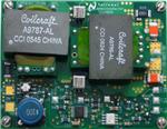
AN-1299 LM5041 Evaluation Board
1
Introduction
The LM5041 evaluation board is designed to provide the design engineer with a fully functional current fed
push-pull power converter to evaluate the LM5041 controller, and also the LM5101 buck stage gate driver,
in a typical environment. Another name often used for the current fed push-pull is a “Cascaded” topology.
The performance of the evaluation board is as follows:
• Input range: 35V to 80V
• Output voltage: 2.5V
• Output current: 0 to 50A
• Measured efficiency: 89% at 50A, 91% at 20A
• Board size: 2.3 × 3.0 × 0.5 inches
• Load Regulation: 0.1%
• Line Regulation: 0.1%
• Line UVLO, Current Limit
The printed circuit board consists of 4 layers of 3 ounce copper on FR4 material with a total thickness of
0.050 inches. Soldermask has been omitted from some areas to facilitate cooling. The unit is designed for
continuous operation at rated load at < 40°C and a minimum airflow of 200 CFM.
2
Theory of Operation
The current fed push-pull converter is a buck type converter consisting of a buck regulation stage followed
by (cascaded by) a push-pull isolation stage that also provides voltage reduction in the transformer. The
buck stage is synchronous, the upper and lower MOSFETS are both N-channel, which are driven by the
LM5101 high voltage buck stage driver. The signals to the driver are provided by the LM5041, which
drives the push-pull stage directly.
The push-pull stage is fed directly from the buck inductor current. The push-pull duty cycles actually
overlap slightly so that there is always a current path for the buck inductor. One cycle of the buck regulator
is provided for each of the push and pull switching events providing proper flux balance in the transformer.
Operating the transformer with both primary windings active during the brief overlap time does not present
a problem to either the current source or the transformer. When both windings are active the
magnetomotive force of the transformer breaks down and the impedance at the VPP node decreases
toward zero. At that time, the inductor source current divides evenly between the primary windings. Some
losses are avoided in the current fed push-pull topology since switching losses require the presence of
both voltage and current.
The output stage uses synchronous rectification to avoid consuming a large percentage of the 2.5 volt
output by the forward voltage drop of a typical Schottky rectifier.
Feedback from the output is processed by an amplifier and reference and then coupled back to the
LM5041 controller through an optocoupler.
All trademarks are the property of their respective owners.
SNVA074A – May 2004 – Revised May 2013
Submit Documentation Feedback
AN-1299 LM5041 Evaluation Board
Copyright © 2004–2013, Texas Instruments Incorporated
1
�Powering and Loading Considerations
www.ti.com
Buck Stage
Push-Pull Stage
VOUT
VPP
35V - 80V
VDD
HB
VCC
VIN
HD
HI
HO
HS
LD
LI
LM5041
LO
LM5101
VSS
PUSH
FEED
BACK
PULL
FB
Figure 1. Simplified Cascaded Push-Pull Converter
3
Powering and Loading Considerations
When applying power to the LM5041 evaluation board certain precautions need to be followed. 125W is a
considerable amount of continuous power. A failure or mistake can present itself in a very alarming
manner. A few simple rules can easily prevent any startling surprises.
4
Proper Connections
When operated at low input voltages the UUT can draw over 4A of current at full load. The maximum
rated output current for the evaluation board is 50A. Be sure to choose the correct connector and wire size
when attaching the source supply and the load. Monitor the current into and out of the UUT (evaluation
board or unit under test). Monitor the voltage directly at the output terminals of the UUT. The voltage drop
across the load connecting wires will give inaccurate measurements. For accurate efficiency
measurements, the same precautions should be taken, attaching a meter directly at the UUT input
terminals.
5
Source Power
The evaluation board can be viewed as a constant power load. At low input line voltage (35V) the input
current can exceed 4A, while at high input line voltage the input current will be approximately 1.8A.
Therefore to fully test the LM5041 evaluation board a DC power supply capable of at least 80V and 5A is
required. The power supply must have adjustments for both voltage and current. An accurate readout of
output current is desirable since the current is not subject to loss in the cables as in the voltage.
The power supply and cabling must present a low impedance to the UUT. Insufficient cabling or a high
impedance power supply will droop during power supply application with the UUT inrush current. If large
enough, this droop will cause a chattering condition upon power up. This chattering condition is an
interaction with the UUT undervoltage lockout, the cabling impedance and the inrush current.
2
AN-1299 LM5041 Evaluation Board
SNVA074A – May 2004 – Revised May 2013
Submit Documentation Feedback
Copyright © 2004–2013, Texas Instruments Incorporated
�Loading
www.ti.com
6
Loading
WARNING
The high temperatures reached by even the most adequately rated
resistors may burn you or melt your benchtop.
An appropriate electronic load specified down to 2.0V is desirable. The resistance of a maximum load is
0.050Ω. You need thick cables! Consult a wire chart if needed. If resistor banks are used there are certain
precautions to be taken. The wattage and current ratings must be adequate for a 50A, 125W supply.
Monitor both current and voltage at all times.
7
Air Flow
Full rated power should never be attempted without providing the specified 200 CFM of air flow over the
UUT. This can be provided by a stand-alone fan.
8
Powering Up
Using the shutdown pin provided will allow powering up the source supply with the current level set low. It
is suggested that the load be kept quite nominal during the first power up. Set the current limit of the
source supply to provide about 1 1/2 times the wattage of the load. As you remove the connection from
the shutdown pin to ground, immediately check for 2.5 volts at the output.
A most common occurrence, that will prove unnerving, is when the current limit set on the source supply is
insufficient for the load. The result is similar to having the high source impedance referred to earlier. The
interaction of the source supply folding back and the UUT going into undervoltage shutdown will start an
oscillation, or chatter, that may have highly undesirable consequences.
A quick efficiency check is the best way to confirm that everything is operating properly. If something is a
miss you can be reasonably sure that it will affect the efficiency adversely. Few parameters can be
incorrect in a switching power supply without creating losses and potentially damaging heat.
Scope
80 Volt, 5 Amp
Power Supply
with Current
Meter
Volt-meter
-
Evaluation Board
+
IN
Volt-meter
Current-meter
+
ON/OFF
(SHUTDOWN)
OUT
200 Watt, 60 Amp
Electrinic Load
-
+
Jumper
Figure 2. Typical Evaluation Setup
SNVA074A – May 2004 – Revised May 2013
Submit Documentation Feedback
AN-1299 LM5041 Evaluation Board
Copyright © 2004–2013, Texas Instruments Incorporated
3
�Performance Characteristics
www.ti.com
9
Performance Characteristics
9.1
Turn-on Waveforms
When applying power to the LM5041 evaluation board a certain sequence of events must occur. Soft-start
capacitor values and other components allow for a minimal output voltage for a short time until the
feedback loop can stabilize without overshoot. Figure 3 and Figure 4 show typical turn-on waveforms at no
load and at a load of 50A. Input voltage, output voltage and output current are shown.
9.2
Output Ripple Waveforms
Figure 5 shows output ripple for a load of 40A. The waveforms should be measured directly across the
output capacitors using a short tip-type ground lead on the scope probe. Bandwidth limiting may also
prove useful.
Trace 1: Input Voltage, no load Volts/div = 10.0V
Trace 2: Output Voltage, no load Volts/div = 1.0V
Trace 3: Output Current, no load Amps/div = 20.0A
Horizontal Resolution = 1µs/div
Figure 3. Typical Turn-on Waveform at No Load
Trace 1: Input Voltage, no loadVolts/div = 10.0V
Trace 2: Output Voltage, no load Volts/div = 1.0V
Trace 3: Output Current, no load Amps/div = 20.0A
Horizontal Resolution = 1µs/div
Figure 4. Typical Turn-on Waveform at a Load of 50A
4
AN-1299 LM5041 Evaluation Board
SNVA074A – May 2004 – Revised May 2013
Submit Documentation Feedback
Copyright © 2004–2013, Texas Instruments Incorporated
�Performance Characteristics
www.ti.com
Conditions: Input Voltage = 48VDC
Output Current = 40A
Bandwidth Limit = 25MHz
Measured Ripple = 90mV pp
Trace 1: Output Ripple Voltage Volts/div = 50mV
Horizontal Resolution = 5µs/div
Figure 5. Output Ripple for a Load of 40A.
Figure 6 shows typical waveforms seen at the buck stage switching node at the input to L2 inductor, trace
3. It also shows the typical waveforms at the push-pull terminals of the main transformer, traces 1 and 2.
The input voltage was 60VDC and the load current was 20.0A.
Figure 7 and Figure 8 show the typical waveforms seen when measuring the drain-source voltage and
current of the push-pull MOSFETS. The upper two traces are the drain-source voltages and the lower two
traces are the corresponding drain-source currents. The input voltage was 48VDC and the load current
was 20.0A. Figure 8 is identical to Figure 7 except for the expanded time scale. The current waveforms
show the characteristic ramp imparted by the buck stage which is responsible for regulation of the output
voltage.
Trace 1: Push-pull at transformer,Side A, load = 20.0A Volts/div = 20.0V
Trace 2: Push-pull at transformer,Side B, load = 20.0A Volts/div = 20.0V
Trace 3: Buck Stage Switching Node, Load = 20.0A Volts/div = 50.0V
Horizontal Resolution = 2µs/div
Figure 6. Typical Waveforms seen at the Buck Stage Switching Node
SNVA074A – May 2004 – Revised May 2013
Submit Documentation Feedback
AN-1299 LM5041 Evaluation Board
Copyright © 2004–2013, Texas Instruments Incorporated
5
�Performance Characteristics
www.ti.com
Trace 1: Push-pull Mosfet drain-source voltage, side A, load = 20.0A Volts/div = 20.0V
Trace 2: Same as trace 1, side B
Trace 3: Push-pull Mosfet drain-source current, side B, load = 20.0A Amps/div = 1.0A
Trace 4: Same as trace 3, side A
Horizontal Resolution = 1µs/div
Figure 7. Typical Waveforms
Trace 1: Push-pull Mosfet drain-source voltage, side A, load = 20.0A Volts/div = 20.0V
Trace 2: Same as trace 1, side B
Trace 3: Push-pull Mosfet drain-source current, side B, load = 20.0A Amps/div = 1.0A
Trace 4: Same as trace 3, side A
Horizontal Resolution = 1µs/div
Figure 8. Typical Waveforms
6
AN-1299 LM5041 Evaluation Board
SNVA074A – May 2004 – Revised May 2013
Submit Documentation Feedback
Copyright © 2004–2013, Texas Instruments Incorporated
�Bill of Materials
www.ti.com
10
Bill of Materials
The Bill of Materials is listed in Table 1 and includes the manufacturer and part number.
Table 1. Bill of Materials
Item
Qty
Part Number
Description
Value
C
1
C4532X7R2A225M
CAPACITOR, CER, TDK
2.2µ, 100V
C
2
C4532X7R2A225M
CAPACITOR, CER, TDK
2.2µ, 100V
C
3
C4532X7R2A225M
CAPACITOR, CER, TDK
2.2µ, 100V
C
4
C4532X7R2A225M
CAPACITOR, CER, TDK
2.2µ, 100V
C
5
C4532X7R3A103K
CAPACITOR, CER, TDK
0.01µ, 1000V
C
6
C0805C471J5GAC
CAPACITOR, CER, KEMET
470p, 50V
C
7
C3216X7R2E104K
CAPACITOR, CER, TDK
0.1µ, 250V
C
8
C4532X7R1E156M
CAPACITOR, CER, TDK
15µ, 25V
C
9
C2012X7R2A103K
CAPACITOR, CER, TDK
0.01µ, 100V
C
10
C2012X7R2E472K
CAPACITOR, CER, TDK
4700p,250V
C
11
C2012X7R1H104K
CAPACITOR, CER, TDK
0.1µ, 50V
C
12
C3216X7R2E104K
CAPACITOR, CER, TDK
0.1µ, 250V
C
13
C0805C101J1GAC
CAPACITOR, CER, KEMET
100p, 100V
C
14
C0805C101J1GAC
CAPACITOR, CER, KEMET
100p, 100V
C
15
C0805C101J1GAC
CAPACITOR, CER, KEMET
100p, 100V
C
16
C2012X7R1H104K
CAPACITOR, CER, TDK
0.1µ, 50V
C
17
C2012X7R1H104K
CAPACITOR, CER, TDK
0.1µ, 50V
C
18
C2012X7R1H104K
CAPACITOR, CER, TDK
0.1µ, 50V
C
19
C2012X7R1H104K
CAPACITOR, CER, TDK
0.1µ, 50V
C
20
C3216X7R1H334K
CAPACITOR, CER, TDK
0.33µ, 50V
C
21
PCC1986CT-ND
CAPACITOR, CER, PANASONIC
1500p, 100V
C
22
PCC1986CT-ND
CAPACITOR, CER, PANASONIC
1500p, 100V
C
23
C3216X7R1H334K
CAPACITOR, CER, TDK
0.33µ, 50V
C
24
C3216X7R1H334K
CAPACITOR, CER, TDK
0.33µ, 50V
C
25
C0805C471J5GAC
CAPACITOR, CER, KEMET
470p, 50V
C
26
C0805C471J5GAC
CAPACITOR, CER, KEMET
470p, 50V
C
27
C3216X7R1H334K
CAPACITOR, CER, TDK
0.33µ, 50V
C
28
T520D337M006AS4350
CAPACITOR,TANT,KEMET
330µ, 6.3V
C
29
T520D337M006AS4350
CAPACITOR,TANT,KEMET
330µ, 6.3V
C
30
C4532X7S0G686M
CAPACITOR, CER, TDK
68µ, 4V
C
31
C4532X7S0G686M
CAPACITOR, CER, TDK
68µ, 4V
C
32
C4532X7S0G686M
CAPACITOR, CER, TDK
68µ, 4V
C
33
C4532X7S0G686M
CAPACITOR, CER, TDK
68µ, 4V
C
34
C2012X7R2A102K
CAPACITOR, CER, TDK
1000p, 100V
C
35
C0805C221J5GAC
CAPACITOR, CER, KEMET
220p, 50V
C
36
C2012X7R2A103K
CAPACITOR, CER, TDK
0.01µ, 100V
C
37
C2012X7R1H104K
CAPACITOR, CER, TDK
0.1µ, 50V
C
38
PCC1996CT-ND
CAPACITOR, CER, PANASONIC
680p, 200V
C
39
C2012X7R1H104K
CAPACITOR, CER, TDK
0.01µ, 50V
C
40
C0805C331J5GAC
CAPACITOR, CER, KEMET
330p, 50V
C
41
C2012X7R2A102K
CAPACITOR, CER, TDK
1000p, 100V
C
42
C1206223K5RAC
CAPACITOR, CER, KEMET
0.022µ, 50V
D
1
CMPD2838-NSA
DIODE, SIGNAL, CENTRAL
D
2
CMPD2838-NSA
DIODE, SIGNAL, CENTRAL
D
3
CMPSH-3C-NSA
DIODE, SIGNAL, CENTRAL
SNVA074A – May 2004 – Revised May 2013
Submit Documentation Feedback
AN-1299 LM5041 Evaluation Board
Copyright © 2004–2013, Texas Instruments Incorporated
7
�Bill of Materials
www.ti.com
Table 1. Bill of Materials (continued)
Item
Qty
Part Number
Description
D
4
BAS56-NSA
DIODE, SIGNAL, CENTRAL
D
5
BAS56-NSA
DIODE, SIGNAL, CENTRAL
D
6
CMPD2838-NSA
DIODE, SIGNAL, CENTRAL
D
7
BAS56-NSA
DIODE, SIGNAL, CENTRAL
D
8
BAS56-NSA
DIODE, SIGNAL, CENTRAL
D
9
CMPD2838-NSA
DIODE, SIGNAL, CENTRAL
D
10
CMPD2838-NSA
DIODE, SIGNAL, CENTRAL
D
11
CMPD2838-NSA
DIODE, SIGNAL, CENTRAL
D
12
CMPD6001S-NSA
DIODE, SIGNAL, CENTRAL
D
13
CRH01CT-ND
DIODE, SIGNAL, TOSHIBA
L
1
SLF12575-100M5R4
L
2
A9787-A, Coilcraft
Value
INPUT CHOKE, TDK
10µH, 5A
PRIMARY CHOKE
60µH, 7.5A
EQ30, Gapped for Al=400, 12Turns, 3C92 material
8
Q
1
SI7456DP
FET, SILICONIX
100V, 25m
Q
2
SI7456DP
FET, SILICONIX
100V, 25m
Q
3
SI7852DP
FET, SILICONIX
80V, 17m
Q
4
SI7852DP
FET, SILICONIX
80V, 17m
Q
5
SI7858DP
FET, SILICONIX
12V, 3m
Q
6
SI7858DP
FET, SILICONIX
12V, 3m
Q
7
SI7858DP
FET, SILICONIX
12V, 3m
Q
8
SI7858DP
FET, SILICONIX
12V, 3m
Q
9
SI7858DP
FET, SILICONIX
12V, 3m
Q
10
SI7858DP
FET, SILICONIX
12V, 3m
Q
11
ZXMN2A03E6
FET, ZETEX
20V, 55m
Q
12
ZXMN2A03E6
FET, ZETEX
20V, 55m
Q
13
ZXMN2A03E6
FET, ZETEX
20V, 55m
Q
14
ZXMN2A03E6
FET, ZETEX
20V, 55m
Q
15
CMPT591E-NSA
PNP, CENTRAL
60V, 1A
Q
16
CMPT591E-NSA
PNP, CENTRAL
60V, 1A
R
1
CRCW12061002F
RESISTOR
10K
R
2
CRCW120610R0F
RESISTOR
10
R
3
CRCW120620R0F
RESISTOR
20
R
4
CRCW12062000F
RESISTOR
200
R
5
CRCW120649R9F
RESISTOR
49.9
R
6
CRCW12061003F
RESISTOR
100K
R
7
CRCW12061001F
RESISTOR
1K
R
8
CRCW12068061F
RESISTOR
8.06K
R
9
CRCW12061652F
RESISTOR
16.5K
R
10
CRCW12062372F
RESISTOR
23.7K
R
11
CRCW12062001F
RESISTOR
2K
R
12
CRCW12064990F
RESISTOR
499
R
13
CRCW12067500F
RESISTOR
750
R
14
CRCW12067500F
RESISTOR
750
R
15
CRCW12065R1J
RESISTOR
5.1
R
16
CRCW12065R1J
RESISTOR
5.1
R
17
CRCW12061002F
RESISTOR
10K
R
18
CRCW12061002F
RESISTOR
10K
AN-1299 LM5041 Evaluation Board
SNVA074A – May 2004 – Revised May 2013
Submit Documentation Feedback
Copyright © 2004–2013, Texas Instruments Incorporated
�Bill of Materials
www.ti.com
Table 1. Bill of Materials (continued)
Item
Qty
Part Number
Description
Value
R
19
CRCW12065R1J
RESISTOR
5.1
R
20
CRCW12065R1J
RESISTOR
5.1
R
21
CRCW2512100J
RESISTOR
10, 1W
R
22
CRCW2512100J
RESISTOR
10, 1W
R
23
CRCW120610R0F
RESISTOR
10
R
24
CRCW120610R0F
RESISTOR
10
R
25
CRCW120610R0F
RESISTOR
10
R
26
CRCW120610R0F
RESISTOR
10
R
27
CRCW12061002F
RESISTOR
10K
R
28
CRCW12061002F
RESISTOR
10K
R
29
CRCW2512100J
RESISTOR
10, 1W
R
30
CRCW2512100J
RESISTOR
10, 1W
R
31
CRCW120610R0F
RESISTOR
10
R
32
CRCW12062102F
RESISTOR
21K
R
33
CRCW12062002F
RESISTOR
20K
R
34
CRCW120610R0F
RESISTOR
10
R
35
CRCW12062002F
RESISTOR
20K
R
36
CRCW12064991F
RESISTOR
4.99K
R
37
CRCW12064991F
RESISTOR
4.99K
R
38
CRCW12061002F
RESISTOR
10K
R
39
CRCW12062002F
RESISTOR
20K
R
40
CRCW2512100J
RESISTOR
10, 1W
R
41
CRCW120610R0F
RESISTOR
10
R
42
CRCW12064991F
RESISTOR
4.99K
R
43
CRCW12061000F
RESISTOR
100
T
1
P8208T, Pulse
CURRENT XFR, PULSE ENG
100:1
T
2
A9786-A, Coilcraft
POWER XFR, COILCRAFT
EQ30, 3C94, 8T,8T,1T,1T,4T
T
3
SM76925, Datatronic
ISOLATION XFR
1:1:1
T
4
SM76925, Datatronic
ISOLATION XFR
1:1:1
U
1
LM5041
CONTROLLER, TEXAS INSTRUMENTS
U
2
LM5101
DUAL HV GATE DRIVER, TEXAS INSTRUMENTS
U
3
MOCD207M
U
4
LM6132
OPAMP, TEXAS INSTRUMENTS
U
5
LM4041
REFERENCE, TEXAS INSTRUMENTS
OPTO-COUPLER, QT OPTO
(4) 1/2 inch STANDOFFs #4
RB 01/21/04
SNVA074A – May 2004 – Revised May 2013
Submit Documentation Feedback
AN-1299 LM5041 Evaluation Board
Copyright © 2004–2013, Texas Instruments Incorporated
9
�PCB Layouts
11
www.ti.com
PCB Layouts
The layers of the printed circuit board are shown in top down order. View is from the top down except for
the bottom silkscreen which is shown viewed from the bottom. Scale is approximately X1.5. The printed
circuit board consists of 4 layers of 3 ounce copper on FR4 material with a total thickness of 0.050 inches.
10
AN-1299 LM5041 Evaluation Board
SNVA074A – May 2004 – Revised May 2013
Submit Documentation Feedback
Copyright © 2004–2013, Texas Instruments Incorporated
�PCB Layouts
www.ti.com
SNVA074A – May 2004 – Revised May 2013
Submit Documentation Feedback
AN-1299 LM5041 Evaluation Board
Copyright © 2004–2013, Texas Instruments Incorporated
11
�PCB Layouts
12
www.ti.com
AN-1299 LM5041 Evaluation Board
SNVA074A – May 2004 – Revised May 2013
Submit Documentation Feedback
Copyright © 2004–2013, Texas Instruments Incorporated
�PCB Layouts
www.ti.com
SNVA074A – May 2004 – Revised May 2013
Submit Documentation Feedback
AN-1299 LM5041 Evaluation Board
Copyright © 2004–2013, Texas Instruments Incorporated
13
�Application Circuit
12
www.ti.com
Application Circuit
Figure 9. Application Circuit: Input 35V to 80V, Output 2.5V, 50A
14
AN-1299 LM5041 Evaluation Board
SNVA074A – May 2004 – Revised May 2013
Submit Documentation Feedback
Copyright © 2004–2013, Texas Instruments Incorporated
�IMPORTANT NOTICE
Texas Instruments Incorporated and its subsidiaries (TI) reserve the right to make corrections, enhancements, improvements and other
changes to its semiconductor products and services per JESD46, latest issue, and to discontinue any product or service per JESD48, latest
issue. Buyers should obtain the latest relevant information before placing orders and should verify that such information is current and
complete. All semiconductor products (also referred to herein as “components”) are sold subject to TI’s terms and conditions of sale
supplied at the time of order acknowledgment.
TI warrants performance of its components to the specifications applicable at the time of sale, in accordance with the warranty in TI’s terms
and conditions of sale of semiconductor products. Testing and other quality control techniques are used to the extent TI deems necessary
to support this warranty. Except where mandated by applicable law, testing of all parameters of each component is not necessarily
performed.
TI assumes no liability for applications assistance or the design of Buyers’ products. Buyers are responsible for their products and
applications using TI components. To minimize the risks associated with Buyers’ products and applications, Buyers should provide
adequate design and operating safeguards.
TI does not warrant or represent that any license, either express or implied, is granted under any patent right, copyright, mask work right, or
other intellectual property right relating to any combination, machine, or process in which TI components or services are used. Information
published by TI regarding third-party products or services does not constitute a license to use such products or services or a warranty or
endorsement thereof. Use of such information may require a license from a third party under the patents or other intellectual property of the
third party, or a license from TI under the patents or other intellectual property of TI.
Reproduction of significant portions of TI information in TI data books or data sheets is permissible only if reproduction is without alteration
and is accompanied by all associated warranties, conditions, limitations, and notices. TI is not responsible or liable for such altered
documentation. Information of third parties may be subject to additional restrictions.
Resale of TI components or services with statements different from or beyond the parameters stated by TI for that component or service
voids all express and any implied warranties for the associated TI component or service and is an unfair and deceptive business practice.
TI is not responsible or liable for any such statements.
Buyer acknowledges and agrees that it is solely responsible for compliance with all legal, regulatory and safety-related requirements
concerning its products, and any use of TI components in its applications, notwithstanding any applications-related information or support
that may be provided by TI. Buyer represents and agrees that it has all the necessary expertise to create and implement safeguards which
anticipate dangerous consequences of failures, monitor failures and their consequences, lessen the likelihood of failures that might cause
harm and take appropriate remedial actions. Buyer will fully indemnify TI and its representatives against any damages arising out of the use
of any TI components in safety-critical applications.
In some cases, TI components may be promoted specifically to facilitate safety-related applications. With such components, TI’s goal is to
help enable customers to design and create their own end-product solutions that meet applicable functional safety standards and
requirements. Nonetheless, such components are subject to these terms.
No TI components are authorized for use in FDA Class III (or similar life-critical medical equipment) unless authorized officers of the parties
have executed a special agreement specifically governing such use.
Only those TI components which TI has specifically designated as military grade or “enhanced plastic” are designed and intended for use in
military/aerospace applications or environments. Buyer acknowledges and agrees that any military or aerospace use of TI components
which have not been so designated is solely at the Buyer's risk, and that Buyer is solely responsible for compliance with all legal and
regulatory requirements in connection with such use.
TI has specifically designated certain components as meeting ISO/TS16949 requirements, mainly for automotive use. In any case of use of
non-designated products, TI will not be responsible for any failure to meet ISO/TS16949.
Products
Applications
Audio
www.ti.com/audio
Automotive and Transportation
www.ti.com/automotive
Amplifiers
amplifier.ti.com
Communications and Telecom
www.ti.com/communications
Data Converters
dataconverter.ti.com
Computers and Peripherals
www.ti.com/computers
DLP® Products
www.dlp.com
Consumer Electronics
www.ti.com/consumer-apps
DSP
dsp.ti.com
Energy and Lighting
www.ti.com/energy
Clocks and Timers
www.ti.com/clocks
Industrial
www.ti.com/industrial
Interface
interface.ti.com
Medical
www.ti.com/medical
Logic
logic.ti.com
Security
www.ti.com/security
Power Mgmt
power.ti.com
Space, Avionics and Defense
www.ti.com/space-avionics-defense
Microcontrollers
microcontroller.ti.com
Video and Imaging
www.ti.com/video
RFID
www.ti-rfid.com
OMAP Applications Processors
www.ti.com/omap
TI E2E Community
e2e.ti.com
Wireless Connectivity
www.ti.com/wirelessconnectivity
Mailing Address: Texas Instruments, Post Office Box 655303, Dallas, Texas 75265
Copyright © 2013, Texas Instruments Incorporated
�


 工商网监
湘ICP备2023018690号
工商网监
湘ICP备2023018690号
