LM5156, LM51561
LM5156,
LM51561
SNVSBI6
– JANUARY
2021
SNVSBI6 – JANUARY 2021
www.ti.com
LM5156x 2.2-MHz Wide VIN 65-V Non-synchronous Boost/SEPIC/Flyback Controller
with Dual Random Spread Spectrum
1 Features
2 Applications
•
•
•
•
•
•
•
•
•
•
•
•
•
•
•
•
•
•
Functional Safety-Capable
– Documentation available to aid functional safety
system design
Suited for wide input operating range battery
applications
– 3.5-V to 60-V operating range (65-V abs max)
– 2.97-V to 16-V when BIAS = VCC
– Minimum boost supply voltage 1.5 V when
BIAS ≥ 3.5 V
– Input transient protection up to 65 V
– Minimized battery drain
• Low shutdown current (IQ ≤ 2.6 µA)
• Low operating current (IQ ≤ 490 µA)
Small solution size and low cost
– Maximum switching frequency of 2.2 MHz
– 12-Pin WSON package (3 mm × 2 mm)
– Integrated error amplifier allows primary-side
regulation without optocoupler (flyback)
EMI mitigation
– Selectable dual random spread spectrum
– Lead-less package
Higher efficiency with low-power dissipation
– 100-mV ±7% accurate current limit threshold
– Strong 1.5-A peak standard MOSFET driver
– Supports external VCC supply
Avoid AM band interference and crosstalk
– Optional clock synchronization
– Dynamically programmable switching frequency
from 100 kHz to 2.2 MHz
Integrated protection features
– Constant peak current limiting over input
voltage
– Optional hiccup mode overload protection (see
the Device Comparison Table)
– Programmable line UVLO
– OVP protection
– Thermal shutdown
±1% accuracy feedback reference
Supports additional slope compensation
Programmable soft start
PGOOD indicator
Create a custom design using the LM5156x with
the WEBENCH® power designer
Multiple-output flyback without optocoupler
LED bias supply
Wide input boost, SEPIC, flyback power module
Portable speaker application
Flyback POE power supply application
Battery-powered boost, SEPIC, flyback
3 Description
The LM5156x (LM5156 and LM51561) device is a
wide input range, non-synchronous boost controller
that uses peak current mode control. The device can
be used in boost, SEPIC, and flyback topologies.
The LM5156x device can start up from a 1-cell battery
with a minimum of 2.97 V if the BIAS pin is connected
to the VCC pin. It can operate with the input supply
voltage as low as 1.5 V if the BIAS pin is greater than
3.5 V.
Device Information
PART NUMBER
PACKAGE(1)
BODY SIZE (NOM)
WSON (12)
3.00 mm × 2.00 mm
LM5156
LM51561
(1)
For all available packages, see the orderable addendum at
the end of the data sheet.
VSUPPLY
VLOAD
BIAS
VCC GATE
UVLO/SYNC
DITHOFF
PGOOD
RT
SS
CS
GND
FB
COMP
Typical Boost Application
An©IMPORTANT
NOTICEIncorporated
at the end of this data sheet addresses availability, warranty, changes, use in
safety-critical
applications,
Copyright
2021 Texas Instruments
Submit
Document
Feedback
intellectual property matters and other important disclaimers. PRODUCTION DATA.
Product Folder Links: LM5156 LM51561
1
�LM5156, LM51561
www.ti.com
SNVSBI6 – JANUARY 2021
Table of Contents
1 Features............................................................................1
2 Applications..................................................................... 1
3 Description.......................................................................1
4 Revision History.............................................................. 2
5 Description (continued).................................................. 3
6 Device Comparison Table...............................................3
7 Pin Configuration and Functions...................................4
8 Specifications.................................................................. 5
8.1 Absolute Maximum Ratings ....................................... 5
8.2 ESD Ratings .............................................................. 5
8.3 Recommended Operating Conditions ........................6
8.4 Thermal Information ...................................................6
8.5 Electrical Characteristics ............................................6
8.6 Typical Characteristics................................................ 9
9 Detailed Description......................................................12
9.1 Overview................................................................... 12
9.2 Functional Block Diagram......................................... 12
9.3 Feature Description...................................................13
9.4 Device Functional Modes..........................................25
10 Application and Implementation................................ 26
10.1 Application Information........................................... 26
10.2 Typical Application.................................................. 26
10.3 System Examples................................................... 31
11 Power Supply Recommendations..............................35
12 Layout...........................................................................36
12.1 Layout Guidelines................................................... 36
12.2 Layout Examples.................................................... 37
13 Device and Documentation Support..........................39
13.1 Device Support....................................................... 39
13.2 Documentation Support.......................................... 39
13.3 Receiving Notification of Documentation Updates..39
13.4 Support Resources................................................. 39
13.5 Trademarks............................................................. 39
13.6 Electrostatic Discharge Caution..............................40
13.7 Glossary..................................................................40
14 Mechanical, Packaging, and Orderable
Information.................................................................... 41
4 Revision History
2
DATE
REVISION
NOTES
January 2021
*
Initial release.
Submit Document Feedback
Copyright © 2021 Texas Instruments Incorporated
Product Folder Links: LM5156 LM51561
�LM5156, LM51561
www.ti.com
SNVSBI6 – JANUARY 2021
5 Description (continued)
The internal VCC regulator also supports BIAS pin operation up to 60 V (65-V absolute maximum) . The
switching frequency is dynamically programmable with an external resistor from 100 kHz to 2.2 MHz. Switching
at 2.2 MHz minimizes AM band interference and allows for a small solution size and fast transient response. To
reduce the EMI of the power supply, the device provides a selectable dual random spread spectrum which
reduces the EMI over the wide frequency range.
The device features a 1.5-A standard MOSFET driver and a low 100-mV current limit threshold. The device also
supports the use of an external VCC supply to improve efficiency. Low operating current and pulse-skipping
operation improve efficiency at light loads.
The device has built-in protection features such as cycle-by-cycle current limit, overvoltage protection, line
UVLO, and thermal shutdown. Hiccup mode overload protection is available in the LM51561 device option.
Additional features include low shutdown IQ, programmable soft start, programmable slope compensation,
precision reference, power-good indicator, and external clock synchronization.
6 Device Comparison Table
DEVICE OPTION
HICCUP MODE PROTECTION
INTERNAL REFERENCE
LM5156
Disabled
1V
LM51561
Enabled
1V
Submit Document Feedback
Copyright © 2021 Texas Instruments Incorporated
Product Folder Links: LM5156 LM51561
3
�LM5156, LM51561
www.ti.com
SNVSBI6 – JANUARY 2021
7 Pin Configuration and Functions
BIAS
1
12
UVLO/SYNC
VCC
2
11
PGOOD
GATE
3
10
RT
4
9
SS
CS
5
8
FB
COMP
6
7
DITHOFF
EP
GND
Figure 7-1. 12-Pin WSON DSS Package (Transparent Top View)
Table 7-1. Pin Functions
PIN
NO.
TYPE(1)
DESCRIPTION
1
BIAS
P
Supply voltage input to the VCC regulator. Connect a bypass capacitor from this pin to GND.
2
VCC
P
Output of the internal VCC regulator and supply voltage input of the MOSFET driver. Connect a
ceramic bypass capacitor from this pin to GND.
3
GATE
O
N-channel MOSFET gate drive output. Connect directly to the gate of the N-channel MOSFET
through a short, low inductance path.
4
GND
G
Ground pin. Connect directly to the ground connection of the sense resistor through a low inductance
wide and short path.
5
CS
I
Current sense input pin. Connect to the positive side of the current sense resistor through a short
path.
6
COMP
O
Output of the internal transconductance error amplifier. Connect the loop compensation components
between this pin and GND.
7
DITHOFF
I
Spread spectrum selection pin. Internal spread spectrum (Clock dithering) is disabled when the pin is
connected to the VCC pin. Connecting the pin to GND enables the internal spread spectrum.
8
FB
I
Inverting input of the error amplifier. Connect a voltage divider from the output to this pin to set output
voltage in boost/SEPIC topologies. Connect the low-side feedback resistor to GND.
9
SS
I
Soft-start time programming pin. An external capacitor and an internal current source set the ramp
rate of the internal error amplifier reference during soft start. Connect the ground connection of the
capacitor to GND.
10
RT
I
Switching frequency setting pin. The switching frequency is programmed by a single resistor
between RT and GND.
11
PGOOD
O
Power-good indicator. An open-drain output which goes low if FB is below the under voltage
threshold. Connect a pullup resistor to the system voltage rail.
Undervoltage lockout programming pin. The converter start-up and shutdown levels can be
programmed by connecting this pin to the supply voltage through a resistor divider. The internal clock
can be synchronized to an external clock by applying a negative pulse signal into the UVLO/
SYNC/EN pin. This pin must not be left floating. Connect to BIAS pin if not used. Connect the lowside UVLO resistor to GND.
12
UVLO/
SYNC/EN
I
—
EP
—
(1)
4
NAME
Exposed pad of the package. The exposed pad must be connected to GND and the large ground
copper plane to decrease thermal resistance.
G = Ground, I = Input, O = Output, P = Power
Submit Document Feedback
Copyright © 2021 Texas Instruments Incorporated
Product Folder Links: LM5156 LM51561
�LM5156, LM51561
www.ti.com
SNVSBI6 – JANUARY 2021
8 Specifications
8.1 Absolute Maximum Ratings
Over the recommended operating junction temperature range(1)
MIN
Input
BIAS to GND
–0.3
65
UVLO to GND
–0.3
VBIAS+0.3
SS to GND(2)
–0.3
3.8
RT to GND(2)
–0.3
3.8
FB to GND
–0.3
4.0
CS to GND(DC)
–0.3
0.3
CS to GND(50ns transient)
Output
-0.3
18
VCC to GND
–0.3
18(3)
GATE to GND (50ns transient)
PGOOD to
GND(4)
Junction temperature, TJ
(6)
Storage temperature, Tstg
(2)
(3)
(4)
(5)
(6)
UNIT
V
–1
DITHOFF to GND
COMP to GND(5)
(1)
MAX
–1
–0.3
18
V
–0.3
–40
150
–55
150
°C
Stresses beyond those listed under Absolute Maximum Ratingsmay cause permanent damage to the device. These are stress ratings
only, which do not imply functional operation of the device at these or any other conditions beyond those indicated under
Recommended Operating Conditions. Exposure to absolute-maximum-rated conditions for extended periods may affect device
reliability.
This pin is not specified to have an external voltage applied.
18 V or VBIAS + 0.3 V whichever is lower
The maximum current sink is limited to 1 mA when VPGOOD>VBIAS.
This pin has an internal max voltage clamp which can handle up to 1.6 mA.
High junction temperatures degrade operating lifetimes. Operating lifetime is de-rated for junction temperatures greater than 125°C.
8.2 ESD Ratings
VALUE
V(ESD)
(1)
(2)
Electrostatic
discharge
Human body model (HBM), per ANSI/ESDA/JEDEC JS-001, all
pins(1)
±2000
Charged device model (CDM), per JEDEC specification JESD22-C101, all pins(2)
±500
UNIT
V
JEDEC document JEP155 states that 500-V HBM allows safe manufacturing with a standard ESD control process.
JEDEC document JEP157 states that 250-V CDM allows safe manufacturing with a standard ESD control process.
Submit Document Feedback
Copyright © 2021 Texas Instruments Incorporated
Product Folder Links: LM5156 LM51561
5
�LM5156, LM51561
www.ti.com
SNVSBI6 – JANUARY 2021
8.3 Recommended Operating Conditions
Over the recommended operating junction temperature range(1)
MIN
Bias input(2)
VBIAS
NOM
2.97
MAX
60
UNIT
V
VVCC
VCC
voltage(3)
2.97
16
V
VDITHOFF
DITHOFF input
0
16
V
VUVLO
UVLO input
0
60
V
VFB
FB input
0
4.0
V
fSW
Typical switching frequency
100
2200
kHz
fSYNC
Synchronization pulse frequency
100
2200
kHz
TJ
Operating junction temperature
–40
125
°C
(1)
(2)
(3)
Operating Ratings are conditions under the device is intended to be functional. For specifications and test conditions, see Electrical
Characteristics.
BIAS pin operating range is from 2.97 V to 16 V when VCC is directly connected to BIAS. BIAS pin operating range is from 3.5 V to 60
V when VCC is supplied from the internal VCC regulator.
This pin voltage should be less than VBIAS + 0.3 V.
8.4 Thermal Information
LM5156x
THERMAL METRIC(1)
DSS(WSON)
UNIT
12 PINS
RθJA
Junction-to-ambient thermal resistance (LM5156EVM-BST)
41.5
°C/W
RθJA
Junction-to-ambient thermal resistance
63.1
°C/W
RθJC(top)
Junction-to-case (top) thermal resistance
62.4
°C/W
RθJB
Junction-to-board thermal resistance
31.6
°C/W
ψJT
Junction-to-top characterization parameter (LM5156EVM-BST)
1.5
°C/W
ψJT
Junction-to-top characterization parameter
2.2
°C/W
ψJB
Junction-to-board characterization parameter (LM5156EVM-BST)
21.8
°C/W
ψJB
Junction-to-board characterization parameter
31.5
°C/W
RθJC(bot)
Junction-to-case (bottom) thermal resistance
10.7
°C/W
(1)
For more information about traditional and new thermal metrics, see the Semiconductor and IC Package Thermal Metrics application
report.
8.5 Electrical Characteristics
Typical values correspond to TJ = 25°C. Minimum and maximum limits apply over TJ = -40°C to 125°C. Unless otherwise
stated, VBIAS = 12 V, RT = 9.09 kΩ
PARAMETER
TEST CONDITIONS
MIN
TYP
MAX
UNIT
SUPPLY CURRENT
ISHUTDOWN(BIAS)
IOPERATING(BIAS)
BIAS shutdown current
VBIAS = 12 V, VUVLO = 0 V
2.6
5
uA
BIAS operating current
VBIAS = 12 V, VUVLO = 2.0 V, VFB =
VREF, RT = 220 kΩ
490
550
uA
6.85
7
VCC REGULATOR
VVCC-REG
VVCC-UVLO(RISING)
IVCC-CL
VCC regulation
VBIAS = 8 V, No load
6.5
VCC regulation
VBIAS = 8 V, IVCC = 35 mA
6.5
VCC UVLO threshold
VCC rising
VCC UVLO hysteresis
VCC falling
VCC sourcing current limit
VBIAS = 10 V, VVCC = 0 V
2.75
2.85
0.063
35
V
V
110
2.95
V
V
mA
ENABLE
6
Submit Document Feedback
Copyright © 2021 Texas Instruments Incorporated
Product Folder Links: LM5156 LM51561
�LM5156, LM51561
www.ti.com
SNVSBI6 – JANUARY 2021
Typical values correspond to TJ = 25°C. Minimum and maximum limits apply over TJ = -40°C to 125°C. Unless otherwise
stated, VBIAS = 12 V, RT = 9.09 kΩ
PARAMETER
TEST CONDITIONS
MIN
TYP
MAX
UNIT
VEN(RISING)
Enable threshold
EN rising
0.4
0.52
0.7
V
VEN(FALLING)
Enable threshold
EN falling
0.33
0.49
0.63
V
VEN(HYS)
Enable hysteresis
EN falling
0.03
V
UVLO/SYNC
VUVLO(RISING)
UVLO / SYNC threshold
UVLO rising
1.425
1.5
1.575
V
VUVLO(FALLING)
UVLO / SYNC threshold
UVLO falling
1.370
1.45
1.520
V
VUVLO(HYS)
UVLO / SYNC threshold
hysteresis
UVLO falling
IUVLO
UVLO hysteresis current
VUVLO = 1.6 V
0.05
4
5
V
6
uA
SPREAD SPECTRUM
VDITHOFF(RISING)
Clock dithering threshold
DITHOFF rising, VBIAS = 4 V
1.1
1.7
2.1
V
VDITHOFF(FALLING)
Clock dithering threshold
DITHOFF falling, VBIAS = 4 V
0.6
1.2
1.8
V
VDITHOFF(HYS)
Clock dithering threshold
hysteresis
DITHOFF falling, VBIAS = 4 V
0.5
V
SS
ISS
Soft-start current
9
SS pull-down switch RDSON
10
11
55
uA
Ω
PULSE WIDTH MODULATION
fsw1
Switching frequency
RT = 220 kΩ, VBIAS = 4 V
85
100
115
kHz
1980
2200
2420
kHz
fsw2
Switching frequency
RT = 9.09 kΩ, VBIAS = 4 V
tON(MIN)
Minimum on-time
RT = 9.09 kΩ
50
ns
DMAX1
Maximum duty cycle limit
RT = 9.09 kΩ, VBIAS = 4 V
80
85
90
%
DMAX2
Maximum duty cycle limit
RT = 220 kΩ, VBIAS = 4 V
90
93
96
%
22.5
30
37.5
uA
93
100
107
mV
CURRENT SENSE
ISLOPE
Peak slope compensation current RT = 220 kΩ
VCLTH
Current Limit threshold (CS-GND)
HICCUP MODE PROTECTION (LM51561)
Hiccup enable cycles
Hiccup timer reset cycles
64
Cycles
8
Cycles
ERROR AMPLIFIER
VREF
FB reference
LM5156, LM51561
0.99
Gm
Transconductance
COMP sourcing current
VCOMP = 1.2 V
180
2.5
1
1.01
2
COMP clamp voltage
COMP rising (VUVLO = 2.0 V)
COMP clamp voltage
COMP falling
Over-voltage threshold
FB rising (referece to VREF)
Over-voltage threshold
FB falling (referece to VREF)
PGOOD pulldown switch RDSON
1 mA sinking
Under-voltage threshold
FB falling (referece to VREF)
Under-voltage threshold
FB rising (referece to VREF)
High-state voltage drop
Low-state voltage drop
V
mA/V
uA
2.8
V
1
1.1
V
110
113
%
OVP
VOVTH
107
105
%
PGOOD
VUVTH
90
87
90
Ω
93
%
95
%
100 mA sinking
0.25
V
100 mA sourcing
0.15
V
MOSFET DRIVER
Submit Document Feedback
Copyright © 2021 Texas Instruments Incorporated
Product Folder Links: LM5156 LM51561
7
�LM5156, LM51561
www.ti.com
SNVSBI6 – JANUARY 2021
Typical values correspond to TJ = 25°C. Minimum and maximum limits apply over TJ = -40°C to 125°C. Unless otherwise
stated, VBIAS = 12 V, RT = 9.09 kΩ
PARAMETER
TEST CONDITIONS
MIN
TYP
MAX
UNIT
THERMAL SHUTDOWN
TTSD
Thermal shutdown threshold
Temperature rising
Thermal shutdown hysteresis
8
Submit Document Feedback
175
°C
15
°C
Copyright © 2021 Texas Instruments Incorporated
Product Folder Links: LM5156 LM51561
�LM5156, LM51561
www.ti.com
SNVSBI6 – JANUARY 2021
8.6 Typical Characteristics
110
2200
108
Frequency, RT=220k: (kHz)
2000
Frequency (kHz)
1800
1600
1400
1200
1000
800
600
106
2280
102
2240
100
2200
98
2160
96
2080
200
90
-40
20
30 40 50 60 70
RT Resistor (k:)
100
2040
-20
0
20
200 250
40
60
80 100
Temperature (qC)
120
140
2000
160
D002
Figure 8-2. Frequency vs Temperature
D001
Figure 8-1. Frequency vs RT Resistance
7
12
6
BIAS
VCC
10
5
Voltage (V)
8
4
3
6
4
2
2
1
0
0
0
20
40
60
IVCC (mA)
80
100
120
0
2
4
D003
Figure 8-3. VVCC vs IVCC
6
VBIAS (V)
8
10
12
D004
Figure 8-4. VVCC vs VBIAS (No Load)
105
20
RSL=0:
RSL=1k:
19
104
Current Limit Threshold (mV)
Peak Inductor Current in Current Limit (A)
2120
RT=9.09kOhm
94
92
910
2320
RT=220kOhm
104
400
0
VVCC (V)
2400
RT=220k:
RT=9.09k: 2360
Frequency, RT=9.09k: (kHz)
2400
18
17
16
15
14
13
12
11
10
20
30
40
50
60
Duty Cycle (%)
70
80
90
102
101
100
99
98
97
96
FSW=440kHz, RS=6m:, LM=1.2PH, VLOAD=10V
10
0
103
100
95
-40
-20
D005
Figure 8-5. Peak Current Limit vs Duty Cycle
0
20
40
60
80 100
Temperature (qC)
120
140
160
D006
Figure 8-6. Current Limit Threshold vs
Temperature
Submit Document Feedback
Copyright © 2021 Texas Instruments Incorporated
Product Folder Links: LM5156 LM51561
9
�LM5156, LM51561
www.ti.com
SNVSBI6 – JANUARY 2021
1.01
1.008
1.004
EN Threshold (V)
FB Reference (V)
1.006
1.002
1
0.998
0.996
0.994
0.992
0.99
-40
-20
0
20
40
60
80 100
Temperature (qC)
120
140
160
0.56
0.55
0.54
0.53
0.52
0.51
0.5
0.49
0.48
0.47
0.46
0.45
0.44
0.43
-40
EN Falling
EN Rising
-20
0
20
40
60
80 100
Temperature (qC)
D007
Figure 8-7. FB Reference vs Temperature
120
140
160
D008
Figure 8-8. EN Threshold vs Temperature
4.5
530
BIAS Shutdown Current (PA)
BIAS Operating Current (PA)
4
520
510
500
490
480
3.5
3
2.5
2
1.5
1
0.5
VFB=VREF, RT=221k:, VVCC=7V, COMP=1.75V
470
0
5
10
15
20
25
30 35
VBIAS (V)
40
45
50
55
60
0
Figure 8-9. IOPERATING(BIAS) Including RT Current vs
VBIAS
15
20
25 30 35
VBIAS (V)
40
45
50
55
60
D010
200
4.4
180
4.2
Minimum On-Time (ns)
BIAS Shutdown Current (PA)
10
Figure 8-10. ISHUTDOWN(BIAS) vs VBIAS
4.6
4
3.8
3.6
3.4
BIAS=12V
BIAS=45V
3.2
3
2.8
2.4
-40
160
140
120
100
80
60
2.6
40
-20
0
20
40
60
80 100
Temperature (qC)
120
140
160
0
250
500
D011
Figure 8-11. ISHUTDOWN vs Temperature
10
5
D009
750 1000 1250 1500 1750 2000 2250 2500
Frequency (kHz)
D012
Figure 8-12. tON(MIN) vs Frequency
Submit Document Feedback
Copyright © 2021 Texas Instruments Incorporated
Product Folder Links: LM5156 LM51561
�LM5156, LM51561
SNVSBI6 – JANUARY 2021
11
2
10.8
1.8
10.6
1.6
Peak Driver Current (A)
Soft-Start Current (PA)
www.ti.com
10.4
10.2
10
9.8
9.6
9.4
-20
0
20
40
60
80 100
Temperature (qC)
120
140
0.6
Isource (A)
Isink (A)
0
160
2
4
6
D013
8
10
VVCC (V)
12
14
16
D014
Figure 8-14. Peak Driver Current vs VCC
95
1.56
UVLO rising
UVLO falling
94
Maximum Duty Cycle Limit (%)
1.54
UVLO Threshold (V)
1
0.8
0.2
Figure 8-13. ISS vs Temperature
1.52
1.5
1.48
1.46
1.44
1.42
1.4
-40
1.2
0.4
9.2
9
-40
1.4
93
92
91
90
89
88
87
86
-20
0
20
40
60
80 100
Temperature (qC)
120
140
160
85
0
250
D015
Figure 8-15. UVLO Threshold vs Temperature
500
750 1000 1250 1500 1750 2000 2250
Frequency (kHz)
D016
Figure 8-16. Maximum Duty Cycle vs Frequency
Submit Document Feedback
Copyright © 2021 Texas Instruments Incorporated
Product Folder Links: LM5156 LM51561
11
�LM5156, LM51561
www.ti.com
SNVSBI6 – JANUARY 2021
9 Detailed Description
9.1 Overview
The LM5156x device is a wide input range, non-synchronous boost controller that uses peak-current-mode
control. The device can be used in boost, SEPIC, and flyback topologies.
The device can start up from a 1-cell battery with a minimum of 2.97 V if the BIAS pin is connected to the VCC
pin. It can operate with the input supply voltage as low as 1.5 V if the BIAS pin is greater than 3.5 V. The internal
VCC regulator also supports BIAS pin operation up to 60 V (65-V absolute maximum) . The switching frequency
is dynamically programmable with an external resistor from 100 kHz to 2.2 MHz. Switching at 2.2 MHz minimizes
AM band interference and allows for a small solution size and fast transient response. To reduce the EMI of the
power supply, the device provides an optional dual random spread spectrum, which reduces the EMI over the
wide frequency span.
The device features a 1.5-A standard MOSFET driver and a low 100-mV current limit threshold. The device also
supports the use of an external VCC supply to improve efficiency. Low operating current and pulse skipping
operation improve efficiency at light loads.
The device has built-in protection features such as cycle-by-cycle current limit, overvoltage protection, line
UVLO, and thermal shutdown. Hiccup mode overload protection is available in the LM51561 device option.
Additional features include low shutdown IQ, programmable soft start, programmable slope compensation,
precision reference, power good indicator, and external clock synchronization.
9.2 Functional Block Diagram
VSUPPLY
D1
LM
VLOAD
CIN
COUT
RFBT
RLOAD
FB
PGOOD
VUVTH
IUVLO
VCC_OK
±
FB
VSUPPLY
VUVLO
RUVLOT
RUVLOB
RFBB
BIAS
+
±
TSD
VOVTH
+
UVLO/
SYNC
VEN
+
RUN
SYNC
Detector
Clock_Sync
VCC_EN
ISS
VCC
Regulator
VCC_EN
+
±
OVP
BIAS
±
VCS1
+
VCSTH
±
TSD
Optional
Hiccup Mode
C/L Comparator
VCC_OK
S
Q
R
Q
VCC
CVCC
VCC
UVLO
GATE
OVP
SS
CSS
VREF
VCS2
+
+
±
Q1
+
ISLOPE
CS
±
GCOMP
FB
COMP
PWM Comparator
Clock
Clock_Sync
Generator
DITHOFF
RCOMP
RT
VCS1
VCS2
RS
GND
RT
CCOMP
12
Submit Document Feedback
Copyright © 2021 Texas Instruments Incorporated
Product Folder Links: LM5156 LM51561
�LM5156, LM51561
www.ti.com
SNVSBI6 – JANUARY 2021
9.3 Feature Description
9.3.1 Line Undervoltage Lockout (UVLO/SYNC/EN Pin)
The device has a dual-level UVLO circuit. During power-on, if the BIAS pin voltage is greater than 2.7 V, and the
UVLO pin voltage is in between the enable threshold (VEN) and the UVLO threshold (VUVLO) for more than 1.5 µs
(see Section 9.3.6 for more details), the device starts up and an internal configuration starts. The device typically
requires a 65-µs internal start-up delay before entering standby mode. In standby mode, the VCC regulator and
RT regulator are operational, SS pin is grounded, and there is no switching at the GATE output.
IUVLO
VSUPPLY
VUVLO
RUVLOT
±
RUN
+
UVLO/
SYNC
VEN
RUVLOB
+
VCC_EN
±
Figure 9-1. Line UVLO and Enable
When the UVLO pin voltage is above the UVLO threshold, the device enters run mode. In the run mode, a softstart sequence starts if the VCC voltage is greater than 4.5 V, or 50 µs after the VCC voltage exceeds the 2.85-V
VCC UV threshold (VVCC-UVLO), whichever comes first. UVLO hysteresis is accomplished with an internal 50-mV
voltage hysteresis and an additional 5-μA current source that is switched on or off. When the UVLO pin voltage
exceeds the UVLO threshold, the current source is enabled to quickly raise the voltage at the UVLO pin. When
the UVLO pin voltage falls below the UVLO threshold, the current source is disabled, causing the voltage at the
UVLO pin to fall quickly. When the UVLO pin voltage is less than the enable threshold (VEN), the device enters
shutdown mode after a 35-µs (typical) delay with all functions disabled.
65-µs (typical)
internal start-up delay
BIAS
= VSUPPLY
50-µs
VCC UV delay
> 3 cycles
2.7 V
1.5 V
0.55 V
Standby
UVLO
Shutdown
VCC
4.5 V
2.85 V
1V
1.5 µs
SS is grounded
with 2 cycles
delay
UVLO should be greater than
0.55 V more than 1.5 µs to start-up
SS
GATE
TSS
SS VLOAD
=
1V
VLOAD(TARGET)
VLOAD
Figure 9-2. Boost Start-Up Waveforms Case 1: Start-Up by 2.85-V VCC UVLO, UVLO Toggle After Start-Up
Submit Document Feedback
Copyright © 2021 Texas Instruments Incorporated
Product Folder Links: LM5156 LM51561
13
�LM5156, LM51561
www.ti.com
SNVSBI6 – JANUARY 2021
50-µs
VCC UV delay
65-µs (typical)
internal start-up delay
> 35 µs
BIAS
= VSUPPLY
65-µs (typical)
internal start-up delay
2.7 V
1.5 V
0.52 V
Standby
UVLO
4.5 V
2.85 V
Shutdown
1V
VCC
1.5 µs
SS is grounded
with 2 cycles
delay
UVLO should be greater than
0.55 V more than 1.5µs to start-up
SS
GATE
tSS
SS VLOAD
=
1V
VLOAD(TARGET)
VLOAD
Figure 9-3. Boost Start-Up Waveforms Case 2: Start-Up When VCC > 4.5 V, EN Toggle After Start-Up
The external UVLO resistor divider must be designed so that the voltage at the UVLO pin is greater than 1.5 V
(typical) when the input voltage is in the desired operating range. The values of RUVLOT and RUVLOB can be
calculated as shown in Equation 1 and Equation 2.
VSUPPLY(ON) u
RUVLOT
VUVLO(FALLING)
VUVLO(RISING)
VSUPPLY(OFF)
IUVLO
(1)
where
•
•
VSUPPLY(ON) is the desired start-up voltage of the converter.
VSUPPLY(OFF) is the desired turnoff voltage of the converter.
RUVLOB
VUVLO(RISING) u RUVLOT
VSUPPLY(ON)
VUVLO(RISING)
(2)
UVLO capacitor (C UVLO) is required in case the input voltage drops below VSUPPLY(OFF) momentarily during startup or during a severe load transient at the low input voltage. If the required UVLO capacitor is large, an
additional series UVLO resistor (RUVLOS) can be used to quickly raise the voltage at the UVLO pin when the 5μA hysteresis current turns on.
14
Submit Document Feedback
Copyright © 2021 Texas Instruments Incorporated
Product Folder Links: LM5156 LM51561
�LM5156, LM51561
www.ti.com
SNVSBI6 – JANUARY 2021
IUVLO
VSUPPLY
VUVLO
RUVLOT
RUVLOS
±
RUN
+
RUVLOB
UVLO/SYNC
CUVLO
Figure 9-4. Line UVLO Using Three UVLO Resistors
Do not leave the UVLO pin floating. Connect to the BIAS pin if not used.
9.3.2 High Voltage VCC Regulator (BIAS, VCC Pin)
The device has an internal wide input VCC regulator which is sourced from the BIAS pin. The wide input VCC
regulator allows the BIAS pin to be connected directly to supply voltages from 3.5 V to 60 V.
The VCC regulator turns on when the device is in the standby or run mode. When the BIAS pin voltage is below
the VCC regulation target, the VCC output tracks the BIAS with a small dropout voltage. When the BIAS pin
voltage is greater than the VCC regulation target, the VCC regulator provides 6.85-V supply for the N-channel
MOSFET driver.
The VCC regulator sources current into the capacitor connected to the VCC pin with a minimum of 35-mA
capability. The recommended VCC capacitor value is from 1 µF to 4.7 µF.
The device supports a wide input range from 3.5 V to 60 V in normal configuration. By connecting the BIAS pin
directly to the VCC pin, the device supports inputs from 2.97 V to 16 V. This configuration is recommended when
the device starts up from a 1-cell battery.
VSUPPLY (2.97V
16V)
BIAS
VLOAD
VCC GATE
UVLO/SYNC
DITHOFF
PGOOD
RT
SS
CS
GND
FB
COMP
Figure 9-5. 2.97-V Start-Up (BIAS = VCC)
The minimum supply voltage after start-up can be further decreased by supplying the BIAS pin from the boost
converter output or from an external power supply as shown in Figure 9-6.
Submit Document Feedback
Copyright © 2021 Texas Instruments Incorporated
Product Folder Links: LM5156 LM51561
15
�LM5156, LM51561
www.ti.com
SNVSBI6 – JANUARY 2021
VSUPPLY
VLOAD
VLOAD
BIAS
UVLO > VUVLO(RISING)
VCC GATE
UVLO/SYNC
DITHOFF
PGOOD
RT
SS
CS
GND
FB
COMP
Figure 9-6. Decrease the Minimum Operating Voltage After Start-Up
In flyback topology, the internal power dissipation of the device can be decreased by supplying the VCC using an
additional transformer winding. In this configuration, the external VCC supply voltage must be greater than the
VCC regulation target (VVCC-REG), and the BIAS pin voltage must be greater the VCC voltage because the VCC
regulator includes a diode between VCC and BIAS.
VSUPPLY
BIAS
VCC GATE
UVLO/SYNC
DITHOFF
PGOOD
RT
SS
CS
GND
FB
COMP
Figure 9-7. External VCC Supply (BIAS ≥ VCC)
If the voltage of the external VCC bias supply is greater than the BIAS pin voltage, use an external blocking
diode from the input power supply to the BIAS pin to prevent the external bias supply from passing current to the
boost input supply through VCC.
9.3.3 Soft Start (SS Pin)
The soft-start feature helps the converter gradually reach the steady state operating point, thus reducing start-up
stresses and surges. The device regulates the FB pin to the SS pin voltage or the internal reference, whichever
is lower.
At start-up, the internal 10-μA soft-start current source (ISS) turns on 50 µs after the VCC voltage exceeds the
2.85-VCC UV threshold, or if the VCC voltage is greater than 4.5 V, whichever comes first. The soft-start current
gradually increases the voltage on an external soft-start capacitor connected to the SS pin. This results in a
gradual rise of the output voltage. The SS pin is pulled down to ground by an internal switch when the VCC is
less than VCC UVLO threshold, the UVLO is less than the UVLO threshold, during hiccup mode off-time or
thermal shutdown.
16
Submit Document Feedback
Copyright © 2021 Texas Instruments Incorporated
Product Folder Links: LM5156 LM51561
�LM5156, LM51561
www.ti.com
SNVSBI6 – JANUARY 2021
In boost topology, soft-start time (tSS) varies with the input supply voltage. The soft-start time in boost topology is
calculated as shown in Equation 3.
tSS
CSS §
VSUPPLY ·
u ¨1
¸
ISS ©
VLOAD ¹
(3)
In SEPIC topology, the soft-start time (tSS) is calculated as follows.
tSS
CSS
ISS
(4)
TI recommends choosing soft-start time long enough so that the converter can start up without going into an
overcurrent state. See Section 9.3.11 for more detailed information.
Figure 9-8 shows an implementation of primary side soft start in flyback topology.
FB
SS COMP
Figure 9-8. Primary-Side Soft Start in Flyback
Figure 9-9 shows an implementation of secondary side soft start in flyback topology.
VLOAD
Secondary Side
Soft-start
Figure 9-9. Secondary-Side Soft Start in Flyback
9.3.4 Switching Frequency (RT Pin)
The switching frequency of the device can be set by a single RT resistor connected between the RT and the
GND pins. The resistor value to set the RT switching frequency (fRT) is calculated as shown in Equation 5.
RT
2.21u 1010
fRT(TYPICAL)
955
(5)
The RT pin is regulated to 0.5 V by the internal RT regulator when the device is enabled.
Submit Document Feedback
Copyright © 2021 Texas Instruments Incorporated
Product Folder Links: LM5156 LM51561
17
�LM5156, LM51561
www.ti.com
SNVSBI6 – JANUARY 2021
9.3.5 Dual Random Spread Spectrum (DRSS)
The device provides a digital spread spectrum which reduces the EMI of the power supply over a wide frequency
range. This function is dynamically selectable during operation. The internal modulator dithers the internal clock
when the DITHOFF pin is less than 1.0 V or the pin is grounded, and it stops clock dithering when the DITHOFF
pin is greater than 2.0 V or the pin is connected to VCC. When an external synchronization clock is applied to
the SYNC pin, the internal spread spectrum is disabled. DRSS (a) combines a low-frequency triangular
modulation profile (b) with a high frequency cycle-by-cycle random modulation profile (c). The low frequency
triangular modulation improves performance in lower radio frequency bands (for example, the AM band), while
the high frequency random modulation improves performance in higher radio frequency bands (for example, the
FM band). In addition, the frequency of the triangular modulation is further modulated randomly to reduce the
likelihood of any audible tones. To minimize output voltage ripple caused by spread spectrum, duty cycle is
modified on a cycle-by-cycle basis to maintain a nearly constant duty cycle when dithering is enabled (see
Figure 9-10).
Frequency
0.156 x fSW
fSW
(a) Low + High Frequency
Random Modulation
(b) Low Frequency
Random Modulation
(c) High Frequency
Random Modulation
DITHER ON
(DITHOFF=GND)
DITHER OFF
(DITHOFF=VCC)
Figure 9-10. Dual Random Spread Spectrum
9.3.6 Clock Synchronization (UVLO/SYNC/EN Pin)
The switching frequency of the device can be synchronized to an external clock by pulling down the UVLO/
SYNC pin. The internal clock of the device is synchronized at the falling edge, but ignores the falling edge input
during the forced off-time which is determined by the maximum duty cycle limit. The external synchronization
clock must pull down the UVLO/SYNC pin voltage below 1.45 V (typical). The duty cycle of the pulldown pulse is
not limited, but the minimum pulldown pulse width must be greater than 150 ns, and the minimum pullup pulse
width must be greater than 250 ns. Figure 9-11 shows an implementation of the remote shutdown function. The
UVLO pin can be pulled down by a discrete MOSFET or an open-drain output of an MCU. In this configuration,
the device stops switching immediately after the UVLO pin is grounded, and the device shuts down 35 µs
(typical) after the UVLO pin is grounded.
VSUPPLY
MCU
UVLO/SYNC
SHUTDOWN
Figure 9-11. UVLO and Shutdown
18
Submit Document Feedback
Copyright © 2021 Texas Instruments Incorporated
Product Folder Links: LM5156 LM51561
�LM5156, LM51561
www.ti.com
SNVSBI6 – JANUARY 2021
Figure 9-12 shows an implementation of shutdown and clock synchronization functions together. In this
configuration, the device stops switching immediately when the UVLO pin is grounded, and the device shuts
down if fSYNC stays in high logic state for longer than 35 µs (typical) (UVLO is in low logic state for more than 35
µs (typical)). The device runs at the fSYNC if clock pulses are provided after the device is enabled.
VSUPPLY
MCU
UVLO/SYNC
FSYNC
Figure 9-12. UVLO, Shutdown, and Clock Synchronization
Duty Cycle [%]
Figure 9-14 and Figure 9-15 show implementations of standby and clock synchronization functions together. In
this configuration, the device stops switching immediately if fSYNC stays in high logic state and enters standby
mode if fSYNC stays in high logic state for longer than two switching cycles. The device runs at fSYNC if clock
pulses are provided. Since the device can be enabled when the UVLO pin voltage is greater than the enable
threshold for more than 1.5 µs, the configurations in Figure 9-14 and Figure 9-15 are recommended if the
external clock synchronization pulses are provided from the start before the device is enabled. This 1.5-µs
requirement can be relaxed when the duty cycle of the synchronization pulse is greater than 50%. Figure 9-13
shows the required minimum duty cycle to start up by synchronization pulses. When the switching frequency is
greater than 1.1 MHz, the UVLO pin voltage should be greater than the enable threshold for more than 1.5 µs
before applying the external synchronization pulse.
80
75
70
65
60
55
50
45
40
35
30
25
20
15
100
200
300
400
500 600 700
fSW [kHz]
800
900 1000 1100
SUby
Figure 9-13. Required Duty Cycle to Start Up by SYNC
VSUPPLY
MCU
UVLO/SYNC
>0.7V
FSYNC
Figure 9-14. UVLO, Standby, and Clock Synchronization (a)
Submit Document Feedback
Copyright © 2021 Texas Instruments Incorporated
Product Folder Links: LM5156 LM51561
19
�LM5156, LM51561
www.ti.com
SNVSBI6 – JANUARY 2021
VSUPPLY
UVLO/SYNC
MCU
FSYNC
Figure 9-15. UVLO, Standby, and Clock Synchronization (b)
If the UVLO function is not required, the shutdown and clock synchronization functions can be implemented
together by using one push-pull output of the MCU. In this configuration, the device shuts down if fSYNC stays in
low logic state for longer than 35 µs (typical). The device is enabled if fSYNC stays in high logic state for longer
than 1.5 µs. The device runs at the fSYNC if clock pulses are provided after the device is enabled. Also, in this
configuration, it is recommended to apply the external clock pulses after the BIAS is supplied. By limiting the
current flowing into the UVLO pin below 1 mA using a current limiting resistor, the external clock pulses can be
supplied before the BIAS is supplied (see Figure 9-16).
MCU
10
UVLO/SYNC
FSYNC
Figure 9-16. Shutdown and Clock Synchronization
Figure 9-17 shows an implementation of inverted enable using external circuit.
VSUPPLY
UVLO/SYNC
LMV431
Figure 9-17. Inverted UVLO
The external clock frequency (fSYNC) must be within +25% and –30% of fRT(TYPICAL). Because the maximum duty
cycle limit and the peak current limit with slope resistor (RSL) are affected by the clock synchronization, take
extra care when using the clock synchronization function. See Section 9.3.7, Section 9.3.8, and Section 9.3.12
for more information.
9.3.7 Current Sense and Slope Compensation (CS Pin)
The device has a low-side current sense and provides both fixed and optional programmable slope
compensation ramps, which help prevent subharmonic oscillation at high duty cycle. Both fixed and
programmable slope compensation ramps are added to the sensed inductor current input for the PWM
20
Submit Document Feedback
Copyright © 2021 Texas Instruments Incorporated
Product Folder Links: LM5156 LM51561
�LM5156, LM51561
www.ti.com
SNVSBI6 – JANUARY 2021
operation, but only the programmable slope compensation ramp is added to the sensed inductor current input
(see Figure 9-18). For an accurate peak current limit operation over the input supply voltage, TI recommends
using only the fixed slope compensation (see Figure 8-5).
The device can generate the programmable slope compensation ramp using an external slope resistor (RSL) and
a sawtooth current source with a slope of 30 μA × fRT. This current flows out of the CS pin.
Current Limit
Comparator
±
ISLOPE
VCSTH
CS
VCS1
+
RSL(optional)
VCS2
+
RF (optional)
RS
CF (optional)
GCOMP =0.142
VSLOPE + offset
±
PWM
Comparator
COMP
RCOMP
CHF
(optional)
CCOMP
Figure 9-18. Current Sensing and Slope Compensation
Programmable Slope
Compensation Ramp
V
Fixed Slope
Compensation
Ramp
ISLOPE × RSL × D
V
Programmable Slope
Compensation Ramp
VSLOPE × D + 0.17V
ISLOPE × RSL × D
Sensed Inductor
Current (RS × ILM)
Figure 9-19. Slope Compensation Ramp (a) at PWM
Comparator Input
Sensed Inductor
Current (RS × ILM)
Figure 9-20. Slope Compensation Ramp (b) at
Current Limit Comparator Input
Use Equation 6 to calculate the value of the peak slope current (ISLOPE) and use Equation 7 to calculate the
value of the peak slope voltage (VSLOPE).
ISLOPE
VSLOPE
30PA u
fRT
fSYNC
40mV u
(6)
fRT
fSYNC
(7)
where
•
fSYNC = fRT if clock synchronization is not used.
Submit Document Feedback
Copyright © 2021 Texas Instruments Incorporated
Product Folder Links: LM5156 LM51561
21
�LM5156, LM51561
www.ti.com
SNVSBI6 – JANUARY 2021
According to peak current mode control theory, the slope of the compensation ramp must be greater than half of
the sensed inductor current falling slope to prevent subharmonic oscillation at high duty cycle. Therefore, the
minimum amount of slope compensation in boost topology should satisfy the following inequality:
0.5 u
VLOAD
VF
VSUPPLY
LM
u RS u Margin
40mV u fSW
(8)
where
•
VF is a forward voltage drop of D1, the external diode
The recommended margin to cover non-ideal factors is 1.2. If required, RSL can be added to further increase the
slope of the compensation ramp. Typically 82% of the sensed inductor current falling slope is known as an
optimal amount of the slope compensation. The RSL value to achieve 82% of the sensed inductor current falling
slope is calculated as shown in Equation 9.
0.82 u
VLOAD
VF
VSUPPLY
LM
u RS
30uA u RSL
40mV u fSW
(9)
If clock synchronization is not used, the fSW frequency equals the fRT frequency. If clock synchronization is used,
the fSW frequency equals the fSYNC frequency. The maximum value for the RSL resistance is 2 kΩ.
9.3.8 Current Limit and Minimum On-time (CS Pin)
The device provides cycle-by-cycle peak current limit protection that turns off the MOSFET when the sum of the
inductor current and the programmable slope compensation ramp reaches the current limit threshold (VCLTH).
Peak inductor current limit (IPEAK-CL) in steady state is calculated as shown in Equation 10.
VCLTH
IPEAK
30PA u RSL u
CL
fRT
fSYNC
uD
RS
(10)
The practical duty cycle is greater than the estimated due to voltage drops across the MOSFET and sense
resistor. The estimated duty cycle is calculated as shown in Equation 11.
D
1
VSUPPLY
VLOAD VF
(11)
Boost converters have a natural pass-through path from the supply to the load through the high-side power
diode (D1). Because of this path and the minimum on-time limitation of the device, boost converters cannot
provide current limit protection when the output voltage is close to or less than the input supply voltage. The
minimum on-time is shown in Figure 8-12 and is calculated as Equation 12.
t ON(MIN) |
800 u 10 15
1
4 u 10
8 u RT
6
(12)
If required, a small external RC filter (RF, CF) at the CS pin can be added to overcome the large leading edge
spike of the current sense signal. Select an RF value in the range of 10 Ω to 200 Ω and a CF value in the range
of 100 pF to 2 nF. Because of the effect of this RC filter, the peak current limit is not valid when the on-time is
less than 2 × RF × CF. To fully discharge the CF during the off-time, the RC time constant should satisfy the
following inequality.
22
Submit Document Feedback
Copyright © 2021 Texas Instruments Incorporated
Product Folder Links: LM5156 LM51561
�LM5156, LM51561
www.ti.com
SNVSBI6 – JANUARY 2021
3 u RF u CF
1 D
fSW
(13)
9.3.9 Feedback and Error Amplifier (FB, COMP Pin)
The feedback resistor divider is connected to an internal transconductance error amplifier which features high
output resistance (RO = 10 MΩ) and wide bandwidth (BW = 7 MHz). The internal transconductance error
amplifier sources current, which is proportional to the difference between the FB pin and the SS pin voltage or
the internal reference, whichever is lower. The internal transconductance error amplifier provides symmetrical
sourcing and sinking capability during normal operation and reduces its sinking capability when the FB is greater
than OVP threshold.
To set the output regulation target, select the feedback resistor values as shown in Equation 14.
VLOAD
§R
VREF u ¨ FBT
© RFBB
·
1¸
¹
(14)
The output of the error amplifier is connected to the COMP pin, allowing the use of a Type 2 loop compensation
network. RCOMP, CCOMP, and optional CHF loop compensation components configure the error amplifier gain and
phase characteristics to achieve a stable loop response. The absolute maximum voltage rating of the FB pin is
3.8 V. If necessary, especially during automotive load dump transient, the feedback resistor divider input can be
clamped with an external zener diode.
The COMP pin features internal clamps. The maximum COMP clamp limits the maximum COMP pin voltage
below its absolute maximum rating even in shutdown. The minimum COMP clamp limits the minimum COMP pin
voltage in order to start switching as soon as possible during no load to heavy load transition. The minimum
COMP clamp is disabled when FB is connected to ground in flyback topology.
9.3.10 Power-Good Indicator (PGOOD pin)
The device has a power-good indicator (PGOOD) to simplify sequencing and supervision. The PGOOD switches
to a high impedance open-drain state when the FB pin voltage is greater than the feedback under voltage
threshold (VUVTH), the VCC is greater than the VCC UVLO threshold and the UVLO/EN is greater than the EN
threshold. A 25-μs deglitch filter prevents any false pulldown of the PGOOD due to transients. The
recommended minimum pullup resistor value is 10 kΩ.
Due to the internal diode path from the PGOOD pin to the BIAS pin, the PGOOD pin voltage cannot be greater
than VBIAS+ 0.3 V.
9.3.11 Hiccup Mode Overload Protection (LM51561 Only)
To further protect the converter during prolonged current limit conditions, the LM51561 device option provides a
hiccup mode overload protection. The internal hiccup mode fault timer of the device counts the PWM clock
cycles when the cycle-by-cycle current limiting occurs after soft start is finished. When the hiccup mode fault
timer detects 64 cycles of current limiting, an internal hiccup mode off-timer forces the device to stop switching
and pulls down SS. Then, the device will restart after 32 768 cycles of hiccup mode off-time. The 64-cycle hiccup
mode fault timer is reset if eight consecutive switching cycles occur without exceeding the current limit threshold.
The soft-start time must be long enough not to trigger the hiccup mode protection after the soft start is finished.
Submit Document Feedback
Copyright © 2021 Texas Instruments Incorporated
Product Folder Links: LM5156 LM51561
23
�LM5156, LM51561
www.ti.com
SNVSBI6 – JANUARY 2021
64 cycles of
current limit
32768 hiccup
mode off cycles
60 cycles of
current limit
7 normal
switching
cycles
4 cycles of
current limit
32768 hiccup
mode off cycles
Inductor Current
Time
Figure 9-21. Hiccup Mode Overload Protection
To avoid an unexpected hiccup mode operation during a harsh load transient condition, it is recommended to
have more margin when programming the peak-current limit.
9.3.12 Maximum Duty Cycle Limit and Minimum Input Supply Voltage
When designing boost converters, the maximum duty cycle should be reviewed at the minimum supply voltage.
The minimum input supply voltage that can achieve the target output voltage is limited by the maximum duty
cycle limit, and it can be estimated as follows.
VSUPPLY(MIN) | VLOAD
VF u 1 DMAX
ISUPPLY(MAX) u RDCR ISUPPLY(MAX) u RDS(ON) RS u DMAX
(15)
where
•
•
•
ISUPPLY(MAX) is the maximum input current
RDCR is the DC resistance of the inductor
RDS(ON) is the on-resistance of the MOSFET
DMAX1
DMAX2
1 0.1u
fSYNC
fRT
(16)
1 100ns u fSW
(17)
The minimum input supply voltage can be further decreased by supplying fSYNC, which is less than fRT. DMAX is
DMAX1 or DMAX2, whichever is lower.
9.3.13 MOSFET Driver (GATE Pin)
The device provides an N-channel MOSFET driver that can source or sink a peak current of 1.5 A. The peak
sourcing current is larger when supplying an external VCC that is higher than 6.75 V VCC regulation target.
During start-up, especially when the input voltage range is below the VCC regulation target, the VCC voltage
must be sufficient to completely enhance the MOSFET. If the MOSFET drive voltage is lower than the MOSFET
gate plateau voltage during start-up, the boost converter may not start up properly and it can stick at the
maximum duty cycle in a high power dissipation state. This condition can be avoided by selecting a lower
threshold N-channel MOSFET switch and setting the VSUPPLY(ON) greater than 6 to 7 V. Because the internal
VCC regulator has a limited sourcing capability, the MOSFET gate charge should satisfy the following inequality.
QG@ VCC u fSW
35mA
(18)
An internal 1-MΩ resistor is connected between GATE and GND to prevent a false turnon during shutdown. In
boost topology, switch node dV/dT must be limited during the 65-µs internal start-up delay to avoid a false
turnon, which is caused by the coupling through CDG parasitic capacitance of the MOSFET.
24
Submit Document Feedback
Copyright © 2021 Texas Instruments Incorporated
Product Folder Links: LM5156 LM51561
�LM5156, LM51561
www.ti.com
SNVSBI6 – JANUARY 2021
9.3.14 Overvoltage Protection (OVP)
The device has OVP for the output voltage. OVP is sensed at the FB pin. If the voltage at the FB pin rises above
the overvoltage threshold (VOVTH), OVP is triggered and switching stops. During OVP, the internal error amplifier
is operational, but the maximum source and sink capability is decreased to 40 µA.
9.3.15 Thermal Shutdown (TSD)
An internal thermal shutdown turns off the VCC regulator, disables switching, and pulls down the SS when the
junction temperature exceeds the thermal shutdown threshold (TTSD). After the temperature is decreased by
15°C, the VCC regulator is enabled again and the device performs a soft start.
9.4 Device Functional Modes
9.4.1 Shutdown Mode
If the UVLO pin voltage is below the enable threshold for longer than 35 µs (typical), the device goes to the
shutdown mode with all functions disabled. In shutdown mode, the device decreases the BIAS pin current
consumption to below 2.6 μA (typical)
9.4.2 Standby Mode
If the UVLO pin voltage is greater than the enable threshold and below the UVLO threshold for longer than 1.5
µs, the device is in standby mode with the VCC regulator operational, RT regulator operational, SS pin
grounded, and no switching at the GATE output. The PGOOD is activated when the VCC voltage is greater than
the VCC UV threshold.
9.4.3 Run Mode
If the UVLO pin voltage is above the UVLO threshold and the VCC voltage is sufficient, the device enters RUN
mode. In this mode, soft start starts 50 µs after the VCC voltage exceeds the 2.85 VCC UV threshold, or if the
VCC voltage is greater than 4.5 V, whichever comes first.
Submit Document Feedback
Copyright © 2021 Texas Instruments Incorporated
Product Folder Links: LM5156 LM51561
25
�LM5156, LM51561
www.ti.com
SNVSBI6 – JANUARY 2021
10 Application and Implementation
Note
Information in the following applications sections is not part of the TI component specification, and TI
does not warrant its accuracy or completeness. TI’s customers are responsible for determining
suitability of components for their purposes, as well as validating and testing their design
implementation to confirm system functionality.
10.1 Application Information
How to Design a Boost Converter Using LM5156x explains how to design boost, SEPIC, and Flyback converters
using the device. This comprehensive application note includes component selections and loop response
optimization.
10.2 Typical Application
Figure 10-1 shows all optional components to design a boost converter.
CSNB
RSNB
LM
VSUPPLY
RBIAS
CBIAS
CIN
DG
CVCC
RUVLOS
BIAS
Q1
VCC GATE
RF
RSL
PGOOD
RT
SS
CF
GND
DITHOFF
RPG
RLOAD
+
±
RFBT
CS
UVLO/SYNC
RUVLOB
MCU_VCC
COUT1 COUT2
D1
RG
RUVLOT
CUVLO
VLOAD
RS
RFBB
FB
COMP
RCOMP CCOMP
RT
CSS
CHF
Figure 10-1. Typical Boost Converter Circuit With Optional Components
10.2.1 Design Requirements
Table 10-1 shows the intended input, output, and performance parameters for this application example.
Table 10-1. Design Example Parameters
DESIGN PARAMETER
VALUE
Minimum input supply voltage (VSUPPLY(MIN))
6V
Target output voltage (VLOAD)
24 V
Maximum load current (ILOAD)
2 A (≈ 48 Watt)
Typical switching frequency (fSW)
440 kHz
10.2.2 Detailed Design Procedure
Use the LM5155x / LM5156x Boost Quick Start Calculator to expedite the process of designing of a regulator for
a given application based on the LM5156x device.
The LM5156x device is also WEBENCH® Designer enabled. The WEBENCH software uses an iterative design
procedure and accesses comprehensive data bases of components when generating a design.
26
Submit Document Feedback
Copyright © 2021 Texas Instruments Incorporated
Product Folder Links: LM5156 LM51561
�LM5156, LM51561
www.ti.com
SNVSBI6 – JANUARY 2021
10.2.2.1 Custom Design With WEBENCH® Tools
Click here to create a custom design using the LM5156x device with the WEBENCH® Power Designer.
1. Start by entering the input voltage (VIN), output voltage (VOUT), and output current (IOUT) requirements.
2. Optimize the design for key parameters such as efficiency, footprint, and cost using the optimizer dial.
3. Compare the generated design with other possible solutions from Texas Instruments.
The WEBENCH Power Designer provides a customized schematic along with a list of materials with real-time
pricing and component availability.
In most cases, these actions are available:
• Run electrical simulations to see important waveforms and circuit performance
• Run thermal simulations to understand board thermal performance
• Export customized schematic and layout into popular CAD formats
• Print PDF reports for the design, and share the design with colleagues
Get more information about WEBENCH tools at www.ti.com/WEBENCH.
10.2.2.2 Recommended Components
Table 10-2 shows a recommended list of materials for this typical application.
Table 10-2. List of Materials (1)
REFERENCE
DESIGNATOR
QTY.
SPECIFICATION
MANUFACTURER
PART NUMBER
RT
1
RES, 49.9 k, 1%, 0.1 W, AEC-Q200 Grade 0, 0603
Vishay-Dale
CRCW060349K9FKEA
RFBT
1
RES, 47.0 k, 1%, 0.1 W, AEC-Q200 Grade 0, 0603
Vishay-Dale
CRCW060347K0FKEA
RFBB
1
RES, 2.0 k, 5%, 0.1 W, AEC-Q200 Grade 0, 0603
Vishay-Dale
CRCW06032K00JNEA
LM
1
Inductor, Shielded, Composite, 6.8 µH, 18.5 A, 0.01 Ω,
SMD
Coilcraft
XAL1010-682MEB
RS
1
RES, 0.008, 1%, 3 W, AEC-Q200 Grade 0, 2512 WIDE
Susumu
KRL6432E-M-R008-F-T1
RSL
1
RES, 0, 5%, 0.1 W, 0603
Yageo America
RC0603JR-070RL
COUT1
3
CAP, CERM, 4.7 µF, 50 V, ±10%, X7R, 1210
TDK
C3225X7R1H475K250AB
COUT2 (Bulk)
2
CAP, Aluminum Polymer, 100 µF, 50 V, ±20%, 0.025 Ω,
AEC-Q200 Grade 2, D10xL10mm SMD
Chemi-Con
HHXB500ARA101MJA0G
CIN1
6
CAP, CERM, 10 µF, 50 V, ±10%, X7R, 1210
MuRata
GRM32ER71H106KA12L
CIN2 (Bulk)
1
CAP, Polymer Hybrid, 100 µF, 50 V, ±20%, 28 Ω, 10x10
SMD
Panasonic
EEHZC1H101P
Q1
1
MOSFET, N-CH, 40 V, 50 A, AEC-Q101, SON-8
Infineon
IPC50N04S5L5R5ATMA1
D1
1
Schottky, 60 V, 10 A, AEC-Q101, CFP15
Nexperia
PMEG060V100EPDZ
RCOMP
1
RES, 11.3 k, 1%, 0.1 W, AEC-Q200 Grade 0, 0603
Vishay-Dale
CRCW060311K3FKEA
CCOMP
1
CAP, CERM, 0.022 µF, 100 V, ±10%, X7R, AEC-Q200
Grade 1, 0603
TDK
CGA3E2X7R2A223K080AA
CHF
1
CAP, CERM, 220 pF, 20 V, ±5%, C0G/NP0, AEC-Q200
Grade 1, 0603
TDK
CGA3E2C0G1H221J080AA
RUVLOT
1
RES, 21.0 k, 1%, 0.1 W, AEC-Q200 Grade 0, 0603
Vishay-Dale
CRCW060321K0FKEA
RUVLOB
1
RES, 7.32 k, 1%, 0.1 W, AEC-Q200 Grade 0, 0603
Vishay-Dale
CRCW06037K32FKEA
RUVLOS
0
N/A
N/A
N/A
CSS
1
CAP, CERM, 0.22 µF, 50 V, ±10%, X7R, AEC-Q200
Grade 1, 0603
TDK
CGA3E3X7R1H224K080AB
DG
0
N/A
N/A
N/A
RG
1
RES, 0, 5%, 0.1 W, 0603
Yageo America
RC0603JR-070RL
CF
1
CAP, CERM, 100 pF, 50 V, ±1%, C0G/NP0, 0603
Kemet
C0603C101F5GACTU
RF
1
RES, 100, 1%, 0.1 W, 0603
Yageo America
RC0603FR-07100RL
Submit Document Feedback
Copyright © 2021 Texas Instruments Incorporated
Product Folder Links: LM5156 LM51561
27
�LM5156, LM51561
www.ti.com
SNVSBI6 – JANUARY 2021
Table 10-2. List of Materials (1) (continued)
REFERENCE
DESIGNATOR
QTY.
SPECIFICATION
MANUFACTURER
PART NUMBER
RSNB
0
N/A
N/A
N/A
CSNB
0
N/A
N/A
N/A
RBIAS
1
RES, 0, 5%, 0.1 W, AEC-Q200 Grade 0, 0603
Panasonic
ERJ-3GEY0R00V
CL10B103KB8NCNC
(1)
CBIAS
1
CAP, CERM, 0.01 µF, 50 V, ±10%, X7R, 0603
Samsung ElectroMechanics
CVCC
1
CAP, CERM, 1 µF, 16 V, ±20%, X7R, AEC-Q200 Grade
1, 0603
MuRata
GCM188R71C105MA64D
RPG
1
RES, 24.9 k, 1%, 0.1 W, 0603
Yageo America
RC0603FR-0724K9L
See Third-party Products Disclaimer
10.2.2.3 Inductor Selection (LM)
When selecting the inductor, consider three key parameters: inductor current ripple ratio (RR), falling slope of the
inductor current, and RHP zero frequency (fRHP).
Inductor current ripple ratio is selected to have a balance between core loss and copper loss. The falling slope of
the inductor current must be low enough to prevent subharmonic oscillation at high duty cycle (additional RSL
resistor is required if not). Higher fRHP (= lower inductance) allows a higher crossover frequency and is always
preferred when using a small value output capacitor.
The inductance value can be selected to set the inductor current ripple between 30% and 70% of the average
inductor current as a good compromise between RR, FRHP, and inductor falling slope.
10.2.2.4 Output Capacitor (COUT)
There are a few ways to select the proper value of output capacitor (COUT). The output capacitor value can be
selected based on output voltage ripple, output overshoot, or undershoot due to load transient.
The ripple current rating of the output capacitors must be enough to handle the output ripple current. By using
multiple output capacitors, the ripple current can be split. In practice, ceramic capacitors are placed closer to the
diode and the MOSFET than the bulk aluminum capacitors to absorb the majority of the ripple current.
10.2.2.5 Input Capacitor
The input capacitors decrease the input voltage ripple. The required input capacitor value is a function of the
impedance of the source power supply. More input capacitors are required if the impedance of the source power
supply is not low enough.
10.2.2.6 MOSFET Selection
The MOSFET gate driver of the device is sourced from VCC. The maximum gate charge is limited by the 35-mA
VCC sourcing current limit.
A leadless package is preferred for high switching-frequency designs. The MOSFET gate capacitance should be
small enough so that the gate voltage is fully discharged during the off-time.
10.2.2.7 Diode Selection
A Schottky is the preferred type for D1 diode due to its low forward voltage drop and small reverse recovery
charge. Low reverse leakage current is an important parameter when selecting the Schottky diode. The diode
must be rated to handle the maximum output voltage plus any switching node ringing. Also, it must be able to
handle the average output current.
10.2.2.8 Efficiency Estimation
The total loss of the boost converter (PTOTAL) can be expressed as the sum of the losses in the device (PIC),
MOSFET power losses (PQ), diode power losses (PD), inductor power losses (PL), and the loss in the sense
resistor (PRS).
28
Submit Document Feedback
Copyright © 2021 Texas Instruments Incorporated
Product Folder Links: LM5156 LM51561
�LM5156, LM51561
www.ti.com
SNVSBI6 – JANUARY 2021
PTOTAL
PIC
PQ
PD
PL
PRS
(19)
PIC can be separated into gate driving loss (PG) and the losses caused by quiescent current (PIQ).
PIC
PG
PIQ
(20)
Each power loss is approximately calculated as follows:
PG
QG(@ VCC) u VBIAS u fSW
PIQ
VBIAS u IBIAS
(21)
(22)
IVIN and IVOUT values in each mode can be found in the supply current section of Section 8.5.
PQ can be separated into switching loss (PQ(SW)) and conduction loss (PQ(COND)).
PQ
PQ(SW )
PQ(COND)
(23)
Each power loss is approximately calculated as follows:
PQ(SW )
0.5 u (VLOAD
VF ) u ISUPPLY u (tR
tF ) u fSW
(24)
tR and tF are the rise and fall times of the low-side N-channel MOSFET device. I SUPPLY is the input supply current
of the boost converter.
PQ(COND)
D u ISUPPLY 2 u RDS(ON)
(25)
RDS(ON) is the on-resistance of the MOSFET and is specified in the MOSFET data sheet. Consider the RDS(ON)
increase due to self-heating.
PD can be separated into diode conduction loss (PVF) and reverse recovery loss (PRR).
PD
PVF
PRR
(26)
Each power loss is approximately calculated as follows:
PVF
(1 D) u VF u ISUPPLY
PRR
VLOAD u QRR u fSW
(27)
(28)
QRR is the reverse recovery charge of the diode and is specified in the diode data sheet. Reverse recovery
characteristics of the diode strongly affect efficiency, especially when the output voltage is high.
PL is the sum of DCR loss (PDCR) and AC core loss (PAC). DCR is the DC resistance of inductor which is
mentioned in the inductor data sheet.
PL
PDCR
PAC
(29)
Submit Document Feedback
Copyright © 2021 Texas Instruments Incorporated
Product Folder Links: LM5156 LM51561
29
�LM5156, LM51561
www.ti.com
SNVSBI6 – JANUARY 2021
Each power loss is approximately calculated as follows:
PDCR
PAC
ISUPPLY 2 u RDCR
(30)
K u 'IE u fSW D
VSUPPLY u D u
'I
(31)
1
fSW
LM
(32)
∆I is the peak-to-peak inductor current ripple. K, α, and β are core dependent factors which can be provided by
the inductor manufacturer.
PRS is calculated as follows:
PRS
D u ISUPPLY 2 u RS
(33)
Efficiency of the power converter can be estimated as follows:
Efficiency
VLOAD u ILOAD
PTOTAL VLOAD u ILOAD
(34)
10.2.3 Application Curve
98
96
94
Efficiency [%]
92
90
88
86
84
82
VSUPPLY=18V
VSUPPLY=12V
VSUPPLY=9V
VSUPPLY=6V
80
78
76
0
0.2
0.4
0.6
0.8
1
1.2
ILOAD [A]
1.4
1.6
1.8
2
BSTE
Figure 10-2. Efficiency
30
Submit Document Feedback
Copyright © 2021 Texas Instruments Incorporated
Product Folder Links: LM5156 LM51561
�LM5156, LM51561
www.ti.com
SNVSBI6 – JANUARY 2021
10.3 System Examples
VSUPPLY
VLOAD
BIAS
VCC GATE
CS
UVLO/SYNC
GND
DITHOFF
PGOOD
RT
FB
SS
COMP
Figure 10-3. Typical Boost Application
VSUPPLY
-
= 3.5V - 60V
VLOAD
+
Car
Battery
BIAS
VCC GATE
CS
PGOOD
GND
Optional
To MCU
From MCU
UVLO/SYNC
DITHOFF
RT
SS
FB
COMP
Figure 10-4. Typical Start-Stop Application
VSUPPLY = 2.97V - 16V
VLOAD = 12V / 24V
+
1-cell or
2-cell
Battery
-
BIAS
VCC GATE
CS
From MCU
PGOOD
GND
UVLO/SYNC
DITHOFF
RT
SS
FB
COMP
Figure 10-5. Emergency-call / Boost On-Demand / Portable Speaker
Submit Document Feedback
Copyright © 2021 Texas Instruments Incorporated
Product Folder Links: LM5156 LM51561
31
�LM5156, LM51561
www.ti.com
SNVSBI6 – JANUARY 2021
VSUPPLY
BIAS
Optional
VLOAD
VCC GATE
CS
UVLO/SYNC
GND
DITHOFF
PGOOD
FB
SS
RT
COMP
Figure 10-6. Typical SEPIC Application
Inductance should be small enough
to operate in DCM at full load
VSUPPLY
BIAS
VLOAD = 30V-150V
VCC GATE
CS
UVLO/SYNC
GND
DITHOFF
PGOOD
FB
SS
RT
From MCU
COMP
Figure 10-7. LIDAR Bias Supply 1
VLOAD > 150V-200V
Voltage
Tripler
VSUPPLY
Inductance should be big enough
to operate in CCM
BIAS
VCC GATE
UVLO/SYNC
GND
DITHOFF
PGOOD
RT
CS
FB
SS
COMP
Figure 10-8. LIDAR Bias Supply 2
32
Submit Document Feedback
Copyright © 2021 Texas Instruments Incorporated
Product Folder Links: LM5156 LM51561
�LM5156, LM51561
www.ti.com
SNVSBI6 – JANUARY 2021
VSUPPLY
VLOAD
BIAS
VCC GATE
UVLO/SYNC
To MCU
(Fault Indicator)
System Power
DITHOFF
PGOOD
RT
SS
CS
GND
FB
COMP
Figure 10-9. Low-Cost LED Driver
VSUPPLY
VLOAD = 5V/12V
BIAS
GATE
UVLO/SYNC
CS
DITHOFF
GND
PGOOD
VCC
RT
FB
SS
COMP
Optional Primary-Side
Soft-Start
Figure 10-10. Secondary-Side Regulated Isolated Flyback
Submit Document Feedback
Copyright © 2021 Texas Instruments Incorporated
Product Folder Links: LM5156 LM51561
33
�LM5156, LM51561
www.ti.com
SNVSBI6 – JANUARY 2021
VLOAD2 = +12V
VSUPPLY
BIAS
VLOAD3 = -8.5V
GATE
CS
UVLO/SYNC
GND
DITHOFF
VCC
To MCU
System Power
PGOOD
RT
SS
COMP
FB
VLOAD1 = 3.3V/5V +/- 2%
Figure 10-11. Primary-Side Regulated Multiple-Output Isolated Flyback
VSUPPLY
VLOAD
BIAS
GATE
UVLO/SYNC
DITHOFF
To MCU
System Power
CS
GND
VCC
PGOOD
RT
SS
COMP
FB
Figure 10-12. Typical Non-Isolated Flyback
34
Submit Document Feedback
Copyright © 2021 Texas Instruments Incorporated
Product Folder Links: LM5156 LM51561
�LM5156, LM51561
www.ti.com
SNVSBI6 – JANUARY 2021
ILED
VSUPPLY
BIAS
VCC GATE
CS
UVLO/SYNC
GND
DITHOFF
PGOOD
RT
FB
SS
COMP
Figure 10-13. LED Driver with High-Side Current Sensing
BIAS
VCC GATE
UVLO/SYNC
To MCU
(Fault Indicator)
System Power
GND
DITHOFF
PGOOD
RT
CS
FB
SS
COMP
TAIL
BRAKE
TURN
BACKUP
TPS9261x
TPS9261x
TPS9261x
TPS9261x
Figure 10-14. Dual-Stage Automotive Rear-Lights LED Driver
11 Power Supply Recommendations
The device is designed to operate from a power supply or a battery whose voltage range is from 1.5 V to 60 V.
The input power supply must be able to supply the maximum boost supply voltage and handle the maximum
input current at 1.5 V. The impedance of the power supply and battery including cables must be low enough that
an input current transient does not cause an excessive drop. Additional input ceramic capacitors can be required
at the supply input of the converter.
Submit Document Feedback
Copyright © 2021 Texas Instruments Incorporated
Product Folder Links: LM5156 LM51561
35
�LM5156, LM51561
www.ti.com
SNVSBI6 – JANUARY 2021
12 Layout
12.1 Layout Guidelines
The performance of switching converters heavily depends on the quality of the PCB layout. The following
guidelines will help users design a PCB with the best power conversion performance, thermal performance, and
minimize generation of unwanted EMI.
•
•
•
•
•
•
•
•
•
•
•
•
•
•
•
•
36
Put the Q1, D1, and RS components on the board first.
Use a small size ceramic capacitor for COUT.
Make the switching loop (COUT to D1 to Q1 to RS to COUT) as small as possible.
Leave a copper area near the D1 diode for thermal dissipation.
Put the device near the RS resistor.
Put the CVCC capacitor as near the device as possible between the VCC and GND pins.
Use a wide and short trace to connect the GND pin directly to the center of the sense resistor.
Connect the CS pin to the center of the sense resistor. If necessary, use vias.
Connect a filter capacitor between CS pin and power ground trace.
Connect the COMP pin to the compensation components (RCOMP and CCOMP).
Connect the CCOMP capacitor to the power ground trace.
Connect the GND pin directly to the analog ground plane. Connect the GND pin to the RUVLOB, RT, CSS, and
RFBB components.
Connect the exposed pad to the GND pin under the device.
Connect the GATE pin to the gate of the Q1 FET. If necessary, use vias.
Make the switching signal loop (GATE to Q1 to RS to GND to GATE) as small as possible.
Add several vias under the exposed pad to help conduct heat away from the device. Connect the vias to a
large ground plane on the bottom layer.
Submit Document Feedback
Copyright © 2021 Texas Instruments Incorporated
Product Folder Links: LM5156 LM51561
�LM5156, LM51561
www.ti.com
SNVSBI6 – JANUARY 2021
12.2 Layout Examples
VSUPPLY
GND
LM
CVIN
Connect
to VSUPPLY
CVIN
Connect
to VSUPPLY
RUVLOB
BIAS
1
12
UVLO
VCC
2
11
PGOOD
GATE
3
10
RT
RT
GND
4
9
SS
CSS
CS
5
8
FB
RFBB
COMP
6
7
DITHOFF
EP
RS
CVCC
Q1
CF
RF
CCOMP
RCOMP
Power Ground Plane
(Connect to EP via GND pin)
RFBT
COUT1
D1
Analog Ground Plane
(Connect to EP)
Thermal Dissipation
Area
RUVLOT
Do not connect input and
output capacitor grounds
underneath the device
Connect
to VLOAD
Do not connect input and
output capacitor grounds
underneath the device
COUT2
Thermal Dissipation
Area
VLOAD
GND
Figure 12-1. PCB Layout Example 1
Submit Document Feedback
Copyright © 2021 Texas Instruments Incorporated
Product Folder Links: LM5156 LM51561
37
�LM5156, LM51561
www.ti.com
SNVSBI6 – JANUARY 2021
LM
VSUPPLY
Thermal Dissipation Area
CVIN
VLOAD
GND
Connect
to VSUPPLY
Do not connect input and
output capacitor grounds
underneath the device
D1
RUVLOT
Thermal Dissipation
Area
Q1
Connect
to VSUPPLY
RUVLOB
BIAS
1
12
UVLO
VCC
2
11
PGOOD
GATE
3
10
RT
RT
GND
4
9
SS
CSS
CS
5
8
FB
RFBB
COMP
6
7
DITHOFF
EP
RS
CVCC
COUT1
COUT2
CF
CCOMP
Power Ground Plane
(Connect to EP via GND pin)
RCOMP
RFBT
RF
Analog Ground Plane
(Connect to EP)
GND
Connect
to VLOAD
Do not connect input and
output capacitor grounds
underneath the device
Figure 12-2. PCB Layout Example 2
38
Submit Document Feedback
Copyright © 2021 Texas Instruments Incorporated
Product Folder Links: LM5156 LM51561
�LM5156, LM51561
www.ti.com
SNVSBI6 – JANUARY 2021
13 Device and Documentation Support
13.1 Device Support
13.1.1 Third-Party Products Disclaimer
TI'S PUBLICATION OF INFORMATION REGARDING THIRD-PARTY PRODUCTS OR SERVICES DOES NOT
CONSTITUTE AN ENDORSEMENT REGARDING THE SUITABILITY OF SUCH PRODUCTS OR SERVICES
OR A WARRANTY, REPRESENTATION OR ENDORSEMENT OF SUCH PRODUCTS OR SERVICES, EITHER
ALONE OR IN COMBINATION WITH ANY TI PRODUCT OR SERVICE.
13.1.2 Development Support
For development support see the following:
• LM5155x / LM5156x Boost Quick Start Calculator
• LM5155x / LM5156x SEPIC Quick Start Calculator
• LM5155x / LM5156x Flyback Quick Start Calculator
13.1.2.1 Custom Design With WEBENCH® Tools
Click here to create a custom design using the LM5156x device with the WEBENCH® Power Designer.
1. Start by entering the input voltage (VIN), output voltage (VOUT), and output current (IOUT) requirements.
2. Optimize the design for key parameters such as efficiency, footprint, and cost using the optimizer dial.
3. Compare the generated design with other possible solutions from Texas Instruments.
The WEBENCH Power Designer provides a customized schematic along with a list of materials with real-time
pricing and component availability.
In most cases, these actions are available:
• Run electrical simulations to see important waveforms and circuit performance
• Run thermal simulations to understand board thermal performance
• Export customized schematic and layout into popular CAD formats
• Print PDF reports for the design, and share the design with colleagues
Get more information about WEBENCH tools at www.ti.com/WEBENCH.
13.2 Documentation Support
13.2.1 Related Documentation
For related documentation see the following:
Texas Instruments, LM5156EVM-BST User's Guide
13.3 Receiving Notification of Documentation Updates
To receive notification of documentation updates, navigate to the device product folder on ti.com. Click on
Subscribe to updates to register and receive a weekly digest of any product information that has changed. For
change details, review the revision history included in any revised document.
13.4 Support Resources
TI E2E™ support forums are an engineer's go-to source for fast, verified answers and design help — straight
from the experts. Search existing answers or ask your own question to get the quick design help you need.
Linked content is provided "AS IS" by the respective contributors. They do not constitute TI specifications and do
not necessarily reflect TI's views; see TI's Terms of Use.
13.5 Trademarks
TI E2E™ is a trademark of Texas Instruments.
WEBENCH® is a registered trademark of Texas Instruments.
All trademarks are the property of their respective owners.
Submit Document Feedback
Copyright © 2021 Texas Instruments Incorporated
Product Folder Links: LM5156 LM51561
39
�LM5156, LM51561
www.ti.com
SNVSBI6 – JANUARY 2021
13.6 Electrostatic Discharge Caution
This integrated circuit can be damaged by ESD. Texas Instruments recommends that all integrated circuits be handled
with appropriate precautions. Failure to observe proper handling and installation procedures can cause damage.
ESD damage can range from subtle performance degradation to complete device failure. Precision integrated circuits may
be more susceptible to damage because very small parametric changes could cause the device not to meet its published
specifications.
13.7 Glossary
TI Glossary
40
This glossary lists and explains terms, acronyms, and definitions.
Submit Document Feedback
Copyright © 2021 Texas Instruments Incorporated
Product Folder Links: LM5156 LM51561
�LM5156, LM51561
www.ti.com
SNVSBI6 – JANUARY 2021
14 Mechanical, Packaging, and Orderable Information
The following pages include mechanical, packaging, and orderable information. This information is the most
current data available for the designated devices. This data is subject to change without notice and revision of
this document. For browser-based versions of this data sheet, refer to the left-hand navigation.
Submit Document Feedback
Copyright © 2021 Texas Instruments Incorporated
Product Folder Links: LM5156 LM51561
41
�PACKAGE OPTION ADDENDUM
www.ti.com
27-Aug-2021
PACKAGING INFORMATION
Orderable Device
Status
(1)
Package Type Package Pins Package
Drawing
Qty
Eco Plan
(2)
Lead finish/
Ball material
MSL Peak Temp
Op Temp (°C)
Device Marking
(3)
(4/5)
(6)
LM51561DSSR
ACTIVE
WSON
DSS
12
3000
RoHS & Green
NIPDAU
Level-1-260C-UNLIM
-40 to 125
2GAH
LM5156DSSR
ACTIVE
WSON
DSS
12
3000
RoHS & Green
NIPDAU
Level-1-260C-UNLIM
-40 to 125
2FUH
(1)
The marketing status values are defined as follows:
ACTIVE: Product device recommended for new designs.
LIFEBUY: TI has announced that the device will be discontinued, and a lifetime-buy period is in effect.
NRND: Not recommended for new designs. Device is in production to support existing customers, but TI does not recommend using this part in a new design.
PREVIEW: Device has been announced but is not in production. Samples may or may not be available.
OBSOLETE: TI has discontinued the production of the device.
(2)
RoHS: TI defines "RoHS" to mean semiconductor products that are compliant with the current EU RoHS requirements for all 10 RoHS substances, including the requirement that RoHS substance
do not exceed 0.1% by weight in homogeneous materials. Where designed to be soldered at high temperatures, "RoHS" products are suitable for use in specified lead-free processes. TI may
reference these types of products as "Pb-Free".
RoHS Exempt: TI defines "RoHS Exempt" to mean products that contain lead but are compliant with EU RoHS pursuant to a specific EU RoHS exemption.
Green: TI defines "Green" to mean the content of Chlorine (Cl) and Bromine (Br) based flame retardants meet JS709B low halogen requirements of
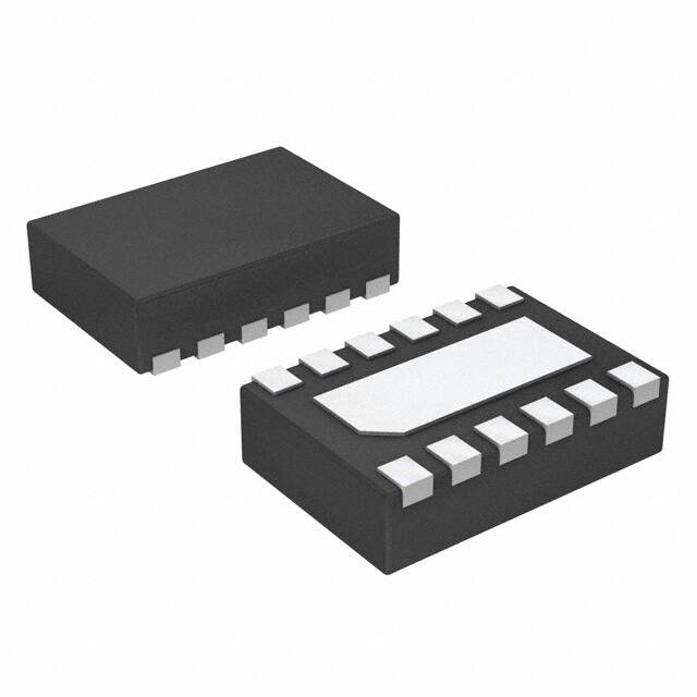


 工商网监
湘ICP备2023018690号
工商网监
湘ICP备2023018690号

