User's Guide
SNVU531A – June 2016 – Revised July 2016
LMR23630A EVM User's Guide
The Texas Instruments LMR23630AEVM evaluation module (EVM) helps designers evaluate the
operation and performance of the LMR23630A wide-input Simple Switcher® buck regulator. This
document describes the setup and the input / output connections of the EVM. Included are the board
layout, schematic, and bill of materials.
1
Introduction
The LMR23630 is a 36 V, 3 A step-down synchronous regulator with 75 µA quiescent current. With a wide
input range from 4.5 V to 36 V, it is suitable for a wide range of applications from automotive to industry
for power conditioning from unregulated sources. The LMR23630AEVM evaluation board is designed to
provide the design engineer to evaluate the LMR23630 series operation and performance.
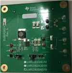
Figure 1. LMR23630AEVM Board
•
•
•
•
•
•
EVM Features
4.5 V to 36 V Input Voltage Range
Jumper Selectable Output Options (5 V or 3.3 V)
Up to 3 A Output Current
Switching Frequency 400 kHz
Frequency Synchronization to External Clock
Hiccup Mode Short Current Protection
The EVM contains one DC-DC converter (See Table 1)
Table 1. Device and Package Configurations
CONVERTER
EVM
IC
PACKAGE
U1
LMR23630AEVM
LMR23630A
HSOIC-8
SNVU531A – June 2016 – Revised July 2016
Submit Documentation Feedback
LMR23630A EVM User's Guide
Copyright © 2016, Texas Instruments Incorporated
1
�Setup
2
www.ti.com
Setup
This section describes the jumpers and connectors on the EVM and how to properly connect, set up and
use the LMR23630AEVM.
2.1
Input/Output Connector Description
VIN — Terminal TP6 – is the power input terminal for the converter. Adjacent to it is the GND reference
ground. Use this terminal to attach the EVM to a cable harness.
VOUT — Terminal TP1 – is the regulated output voltage for the converter. Adjacent to it is the GND
reference ground.
GND — Terminal TP4, TP7 – are the ground reference for the converter. Use these terminals to attach
the EVM to a cable harness.
EN — Jumper J1 – is used to enable the switch-mode converter. The device will be enabled when the
respective jumper is high or floating, and disabled when low. The EVM default system UVLO is 6.2 V
(typical), it also can be programmed by changing R3 or R6. Refer to LMR23630A datasheet for enable
and adjustable undervoltage lockout.
J1
J1
GND
EN
Disable
GND
EN
Enabled by
VIN UVLO
J1
GND
EN
Enabled by
System UVLO
Figure 2. Enable Jumper Setting
SYNC — Jumper J2 – is used to synchronize the switching frequency to external clock. Refer to
datasheet for detail application information.
Testpoint — TP2, TP3, TP5, TP8, TP9, TP10, TP11 – these are test points used for input/output voltage
measurements and loop response measurements.
2.2
Adjusting the Output Voltage
The default setting output voltage is 5.0 V. Open J3 will change output voltage from 5 V to 3.3 V.
If other outputs need to be configured, then: open J3 and adjust the feedback resistors using the following
equation.
VOUT = VREF × ( 1 + ( R4 / R5 ) )
where
•
3
VREF is 1 V
(1)
Board Layout
Figure 3 to Figure 6 show the board layout for the LMR23630AEVM. The PCB consists of a 4-layer
design. 2-oz copper planes are applied on all four layers to dissipate heat with an array of thermal vias
under the thermal pad to connect to all four layers.
2
LMR23630A EVM User's Guide
SNVU531A – June 2016 – Revised July 2016
Submit Documentation Feedback
Copyright © 2016, Texas Instruments Incorporated
�Board Layout
www.ti.com
Figure 3. Top Layer
Figure 4. Middle Layer 1
SNVU531A – June 2016 – Revised July 2016
Submit Documentation Feedback
LMR23630A EVM User's Guide
Copyright © 2016, Texas Instruments Incorporated
3
�Board Layout
www.ti.com
Figure 5. Middle Layer 2
Figure 6. Bottom Layer
4
LMR23630A EVM User's Guide
SNVU531A – June 2016 – Revised July 2016
Submit Documentation Feedback
Copyright © 2016, Texas Instruments Incorporated
�Schematic and Bill of Materials
www.ti.com
4
Schematic and Bill of Materials
Figure 7. LMR23630AEVM Schematic
SNVU531A – June 2016 – Revised July 2016
Submit Documentation Feedback
LMR23630A EVM User's Guide
Copyright © 2016, Texas Instruments Incorporated
5
�Schematic and Bill of Materials
www.ti.com
Table 2. LMR23630AEVM Bill of Materials (BOM)
Designator
Description
Part Number
Footprint
C1
CAP, TA, 150 µF, 16 V, +/- 20%, 0.015 ohm, SMD
T530X157M016ATE015
7343-43
1
C2
CAP, CERM, 1 μF, 25 V, +/- 10%, X7R, 0805
GRM219R71E105KA88D
0805
1
C3
CAP, CERM, 47 μF, 16 V, +/- 20%, X5R, 1210
GRM32ER61C476ME15L
1210
1
C5
CAP, CERM, 0.22 μF, 50 V, +/- 10%, X7R, 0805
GRM21BR71H224KA01L
0805
1
C6, C7
CAP, CERM, 4.7 μF, 50 V, +/- 10%, X7R, 1210
GRM32ER71H475KA88L
1210
2
C9
CAP, CERM, 0.47 μF, 16 V, +/- 10%, X7R, 0603
GRM188R71C474KA88D
0603
1
C10
CAP, CERM, 2.2 μF, 16 V, +/- 10%, X7R, 0603
GRM188Z71C225KE43
0603
1
C11
CAP, CERM, 1000 pF, 50 V, +/- 10%, X7R, 0603
GRM188R71H102KA01D
0603
1
J1
Header, 100mil, 3x1, Gold, TH
TSW-103-07-G-S
TSW-103-07-G-S
1
J2, J3
Header, 100mil, 2x1, Gold, TH
TSW-102-07-G-S
TSW-102-07-G-S
2
L3
Inductor, Wirewound, Metal Composite, 8.2 µH, 5.05 A,
0.0286 ohm, SMD
7447797820
WE-PDF-1045
1
R1
RES, 0, 5%, 0.1 W, 0603
CRCW06030000Z0EA
0603
1
R2
RES, 49.9, 1%, 0.1 W, 0603
CRCW060349R9FKEA
0603
1
R3
RES, 402 k, 1%, 0.1 W, 0603
CRCW0603402KFKEA
0603
1
R4
RES, 53.6k, 1%, 0.1W, 0603
CRCW060353K6FKEA
0603
1
R5
RES, 23.2 k, 1%, 0.1 W, 0603
CRCW060323K2FKEA
0603
1
R6
RES, 133 k, 1%, 0.1 W, 0603
CRCW0603133KFKEA
0603
1
R7
RES, 31.6 k, 1%, 0.1 W, 0603
CRCW060331K6FKEA
0603
1
SH-J1, SH-J3
Shunt, 100 mil, Flash Gold, Black
SPC02SYAN
SPC02SYAN
2
TP1, TP4, TP6,
TP7
Terminal, Turret, TH, Double
1502-2
Keystone1502-2
4
TP2, TP5, TP9
Test Point, Compact, Red, TH
5005
Keystone5005
3
TP3, TP8, TP11
Test Point, Compact, Black, TH
5006
'Keystone5006
3
Test Point, Compact, Orange, TH
5008
Keystone5008
1
SIMPLE SWITCHER 36 V, 3 A Synchronous StepDown Converter, DDA0008E
LMR23630ADDAR
HSOIC-8
1
PCB, FR4, 4 Layers, Size 3000 x 3000 mil, Thickness
62 mil
SV601280
TP10
U1
PCB
6
Quantity
LMR23630A EVM User's Guide
1
SNVU531A – June 2016 – Revised July 2016
Submit Documentation Feedback
Copyright © 2016, Texas Instruments Incorporated
�Revision History
www.ti.com
Revision History
NOTE: Page numbers for previous revisions may differ from page numbers in the current version.
Changes from Original (June 2016) to A Revision ......................................................................................................... Page
•
Changed the minimum input voltage spec from 4V to 4.5V as required through the document. ............................... 1
SNVU531A – June 2016 – Revised July 2016
Submit Documentation Feedback
Revision History
Copyright © 2016, Texas Instruments Incorporated
7
�IMPORTANT NOTICE AND DISCLAIMER
TI PROVIDES TECHNICAL AND RELIABILITY DATA (INCLUDING DATASHEETS), DESIGN RESOURCES (INCLUDING REFERENCE
DESIGNS), APPLICATION OR OTHER DESIGN ADVICE, WEB TOOLS, SAFETY INFORMATION, AND OTHER RESOURCES “AS IS”
AND WITH ALL FAULTS, AND DISCLAIMS ALL WARRANTIES, EXPRESS AND IMPLIED, INCLUDING WITHOUT LIMITATION ANY
IMPLIED WARRANTIES OF MERCHANTABILITY, FITNESS FOR A PARTICULAR PURPOSE OR NON-INFRINGEMENT OF THIRD
PARTY INTELLECTUAL PROPERTY RIGHTS.
These resources are intended for skilled developers designing with TI products. You are solely responsible for (1) selecting the appropriate
TI products for your application, (2) designing, validating and testing your application, and (3) ensuring your application meets applicable
standards, and any other safety, security, or other requirements. These resources are subject to change without notice. TI grants you
permission to use these resources only for development of an application that uses the TI products described in the resource. Other
reproduction and display of these resources is prohibited. No license is granted to any other TI intellectual property right or to any third
party intellectual property right. TI disclaims responsibility for, and you will fully indemnify TI and its representatives against, any claims,
damages, costs, losses, and liabilities arising out of your use of these resources.
TI’s products are provided subject to TI’s Terms of Sale (www.ti.com/legal/termsofsale.html) or other applicable terms available either on
ti.com or provided in conjunction with such TI products. TI’s provision of these resources does not expand or otherwise alter TI’s applicable
warranties or warranty disclaimers for TI products.
Mailing Address: Texas Instruments, Post Office Box 655303, Dallas, Texas 75265
Copyright © 2019, Texas Instruments Incorporated
�


 工商网监
湘ICP备2023018690号
工商网监
湘ICP备2023018690号
