LMX2581EVM
User's Guide
Literature Number: SNAU136C
November 2012 – Revised November 2013
�User's Guide
SNAU136C – November 2012 – Revised November 2013
LMX2581EVM User's Guide
The Texas Instruments LMX2581EVM evaluation module (EVM) helps designers evaluate the operation
and performance of the LMX2581 Wideband Frequency Synthesizer. The EVM contains one Frequency
Synthesizer.
Converter: U1
IC: LMX2581
Package: LQA32A
Topic
1
2
3
4
5
6
2
...........................................................................................................................
Page
Setup ................................................................................................................. 3
Using the EVM Software ...................................................................................... 5
Board Construction ............................................................................................. 9
PCB Layers ...................................................................................................... 15
Measured Performance Data ............................................................................... 20
Bill of Materials ................................................................................................. 39
LMX2581EVM User's Guide
SNAU136C – November 2012 – Revised November 2013
Submit Documentation Feedback
Copyright © 2012–2013, Texas Instruments Incorporated
�Setup
www.ti.com
1
Setup
1.1
Input and Output Connector Description
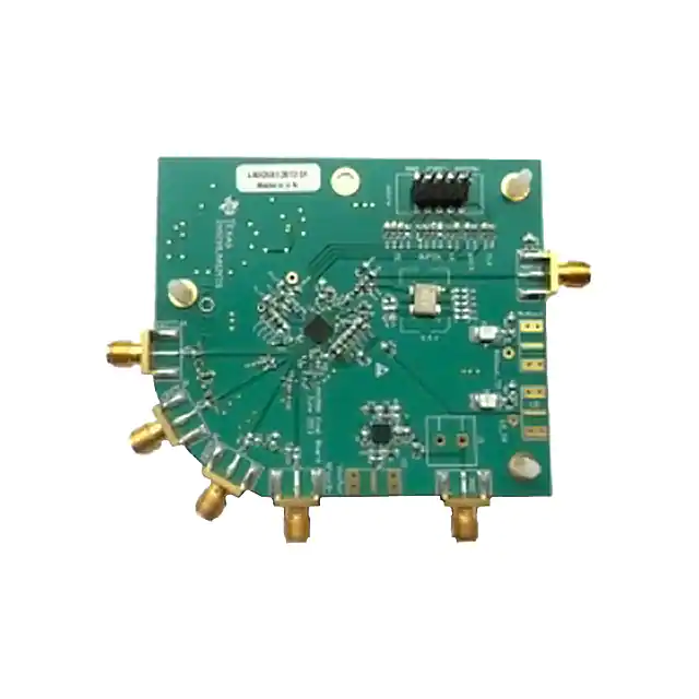
Figure 1. Evaluation Board Setup
Table 1. Inputs and Outputs
Output Name(s)
1.2
Input/Output
Required?
Function
RFoutA+/RFoutARFoutB+/RFoutB
Output
Required
These are two differential outputs. Connect any of the four
outputs to a spectrum analyzer or phase noise analyzer. It is
recommended to put a 50 ohm terminator for the unused side of
the differential output. Failure to do so will degrade
performance, especially output power and harmonics. The
Agilent E5052A was used for these instructions.
V CC
Input
Required
Connect to a 3.3 V Power Supply. Ensure the current limit is set
above 300 mA.
V CC Aux
Input
Optional
This gives the option to supply power to an external VCO.
Programming
Interface
Input
Required
Connect the board to a PC using the provided cable.
OSCin
Input
Optional
The on-board 100 MHz XO has been enabled. To disable the
XO and utilize the OSCin port move R13 to R12 and disconnect
R4 (removing power from the XO).
Installing the EVM Software
Go to http://www.ti.com/tool/codeloader and download and run the most current software.
SNAU136C – November 2012 – Revised November 2013
Submit Documentation Feedback
Copyright © 2012–2013, Texas Instruments Incorporated
LMX2581EVM User's Guide
3
�Setup
1.3
www.ti.com
Loop Filter Values and Configuration Information
Table 2. Loop Filter values and Configuration
Category
Configuration
VCO Gain
Loop Filter Components
Loop Filter Characteristics
Parameter
Value
OSCin Frequency (MHz)
100 MHz
Phase Detector Frequency (MHz)
20 MHz
VCO Frequency
1850 to 3760 MHz
Charge Pump Gain
2400 µA
VCO Core 1
15 to 25 MHz/V
VCO Core 2
18 to 32 MHz/V
VCO Core 3
23 to 40 MHz/V
VCO Core 4
26 to 46 MHz/V
C1_LF
1.8 nF
C2_LF
56 nF
C3_LF
Open
C4_LF
3.3 nF
R2_LF
390 Ω
R3_LF
270 Ω
R4_LF
0
Loop Bandwidth
28.7 kHz
Phase Margin
49.7°
Note that C4_LF is placed and C3_LF is left off because C4_LF is closer to the Vtune input. It is
recommended that the capacitor next to the VCO be at least 3.3 nF for optimal VCO phase noise. If this
constraint is violated, then there can be some degradation in the VCO phase noise in the 200kHz to 1
MHz region, depending on how much smaller than 3.3 nF this capacitor is.
1.4
Burning in the Crystal Oscillator
To get the best stability and phase noise from this XO, it is recommended to let the board run for several
in order burn in the crystal oscillator.
Noise before burning in.
Noise after burning in XO.
Figure 2. Impact of Burning in the XO
4
LMX2581EVM User's Guide
SNAU136C – November 2012 – Revised November 2013
Submit Documentation Feedback
Copyright © 2012–2013, Texas Instruments Incorporated
�Using the EVM Software
www.ti.com
2
Using the EVM Software
2.1
Main Setup and Default Mode
NOTE: To restore the device to its default settings at any time, load the default mode from the “Modes”
menu.
Figure 3. Loading Default Mode for the Main Configuration Screen
SNAU136C – November 2012 – Revised November 2013
Submit Documentation Feedback
Copyright © 2012–2013, Texas Instruments Incorporated
LMX2581EVM User's Guide
5
�Using the EVM Software
2.2
www.ti.com
Loading the Device
To load the settings for the first time, you can either load this from the main menu as shown above or
press +L. When the frequency or programmable bit settings are changed, CodeLoader will
change the register associated with that programmable bit or change, but not all the registers.
Although the GUI shows the
outputs being divided, the output
frequency will be the VCO
frequency unless the OUTx_MUX
bits on the Bits/Pins page are set
Figure 4. Loading the device
6
LMX2581EVM User's Guide
SNAU136C – November 2012 – Revised November 2013
Submit Documentation Feedback
Copyright © 2012–2013, Texas Instruments Incorporated
�Using the EVM Software
www.ti.com
2.3
Port Setup
On the Port Setup tab, the user may select the type of communication port (USB or Parallel) that will be
used to program the device on the evaluation board. If parallel port is selected, the user should ensure
that the correct port address is entered. CodeLoader does NOT auto detect the correct settings for this.
Also note that the BUFEN pin does not work with the USB2ANY board because pin location 5 is reserved
for other purposes. Be aware that the board has been revised and the port setup has changed.
Figure 5.
SNAU136C – November 2012 – Revised November 2013
Submit Documentation Feedback
Copyright © 2012–2013, Texas Instruments Incorporated
LMX2581EVM User's Guide
7
�Using the EVM Software
2.4
www.ti.com
Bits/Pins Settings
To view the function of any bit on the CodeLoader configuration tabs, place the cursor over the desired bit
register label and click the right mouse button on it for a description.
If used with the USB2ANY
board, the BUFEN pin will not
work due to address conflict.
BUFEN_DIS chooses to ignore
this pin and always power up
buffer.
Right mouse click on any bit to
get a description of its function.
The VCO Divider will be
ignored unless this is changed
to “Channel Divider”
Figure 6. Bits/Pins Settings
8
LMX2581EVM User's Guide
SNAU136C – November 2012 – Revised November 2013
Submit Documentation Feedback
Copyright © 2012–2013, Texas Instruments Incorporated
�Board Construction
www.ti.com
3
Board Construction
3.1
Board Layer Stack Up
The board is made on FR4 for the Prepreg and Core Layers. The top layer is 1 oz copper.
Total Height (60.8mil)
Prepreg (16mil)
Top Layer
Core (22mil)
GND
Prepreg (16mil)
Power
Bottom Layer
Figure 7. Board Layer Stack Up
FR4 material was chosen because of convenience, availability, and cost. If one was to use Rogers 4003
on the top Prepreg layer, the output power improves about 1 dB. Otherwise, the performance is very
similar.
SNAU136C – November 2012 – Revised November 2013
Submit Documentation Feedback
Copyright © 2012–2013, Texas Instruments Incorporated
LMX2581EVM User's Guide
9
�Board Construction
Schematic
2
R5
DNP
R6
0
10
VccPlane
OUT
VccAux
R15
DNP
R34
DNP
0
MUXout
R32
DNP
0
1 DNP
C10
C9
0
R20
D1
100pF
0
DNP
0
28
30
29
32
D2
0
C
100pF
GND
PAD
VccPlane
12k
0
12k
R41 R42 R44 R43
DNPC22
DNP
10k 10k
12k 12k
C105 DNP
DNP
GND
Vtune
GND
GND
DNP
2
4
6
8
10
5
6
7
8
VccPlane
GND
GND
RFout
GND
12
11
10
9
18
18
U100
uWire
52601-S10-8LF
1
3
5
7
9
R45
DNP
GND
LD
BUFEN
VCCDIG
OSCin
MUXout
GND
16
15
14
12
13
2.2µF
Vtune
C4_LF
3300pF
19
C16
2.2µF
18
VccPlane
17
0
R28
0
C17
R29
100pF
VccPlane
R27
0
Mechanical Information
C
- Standoffs are mounted in holes in the board
S1
100pF
TCBS-6-01
PCB
LOGO
ESD Susceptible
S2
C108
DNP
TCBS-6-01
PCB
LOGO
S3
Texas Instruments
100pF
L2
TCBS-6-01
R26
51
100pF
5
4
3
2
RFoutA+
142-0701-851
18nH
51
R23
C23
C107
DNP
L1
S4
C26
C24
18nH
C25
100pF
100pF
5
4
3
2
RFoutA142-0701-851
TCBS-6-01
C28
C27
100pF
5
4
3
2
100pF
100pF
5
4
3
2
RFoutB+
142-0701-851
S5
TCBS-6-01
PCB Number: SV601009
PCB Rev: A
RFoutB142-0701-851
VccPlane
R46
10k
100pF
C19
R112
0
DNP
- An external VCO can be used to hit the most demanding phase noise specifications.
0
21
20
VccPlane
External VCO
MUXout_uWire
D
C31
0.1µF
C15
VccPlane
Fin
1592820000
100pF
R109
DNP
100pF
LD_uWire
C30
10µF
22µF
16
15
14
13
1µF
1
2
3
4
Vcc_TB
1
2
22
0
GND
GND
Vcc
GND
R40
C29
C14
R24
R110
DNP
68
R111
DNP
142-0701-851
VccPlane
10µF
120 ohm
1
10k
12k
R39
C104
DNP
R106
DNP
DNP
DNP
GND
GND
GND
GND
R35 R36 R37 R38
10k
R105
DNP
0
CE
10µF
DNPC7 R9
0.01µF866DNP
C18
LMX2581SQ/NOPB
0
VccPlane
VCCVCO
L4
U1
R25
0
0
CLK
11
VccAux
R107
DNP
R108
DNP
DATA
GND
GND
3300pF
C106
DNP
LE
VbiasVCO
CPout
DNP
Vtune_TP
270
DNPC3_LF
C6
1µF
24
23
1
DNP DNP
C100 R102
Open
DNP
0.056µF
C5
2.00k
3
B
1
Open
R3_LF
VCCCP
VCCBUF
R4_LF
Vtune
GND
Vtune
C2_LF
GND
FLout
9
3
8
Open
R101
DNP
7
100pF
CE
RFoutB-
6
C20
R100
DNP
VccPlane
U101
2
4
5
R22
1800pF
4
V+
V-
DNP
VccPlane
0
DNP
DNP
390
VrefVCO
10
1
R2pLF
DNP
Vcc
1
0
22µF
C13
LE
1
5
Open
CE
390
C1_LF
1
R12
C11
VbiasCOMP
RFoutB+
DNP
BYP
GND
C4
DNP
DNP
R10
10µF
VregVCO
DATA
RFoutA-
R2_LF
C103
DNP
C101
DNP
LM6211MF
FLout_TP
3
CLK
RFoutA+
LE
2
Fin
Open
1
VCCFRAC
CLK
DATA
DNP
NC
NC
DAP
0
2200pF
6
C12
VCCPL
Loop Filter
ADJ
142-0701-851
100pF
R104
DNP
OUT
SD
DNP
R31
330
BUFEN
31
Green
B
2
7
9
VccPlane
R11
DNP
5
IN
Green
R21
C109
DNP
8
LP3878SD-ADJ
1
C8
100pF
VccPlane
120 ohm
LD
DNP
R18
0 C110
100pF
DNP
0
R19
2
3
4
5
R33
DNP
330
142-0701-851
GND_OSC
R103
DNP
51k
LD_TP
R17
DNP
VccAux
4.7µF
VccPlane
L3
DNP
4
R8
DNP
DNPC3
142-0701-851
33
MUXout_TP
Y1 is for a XO, but has
accomodations also for
VCXOs as well.
C102
DNP
0
GND_OSC
R16
GND_OSC
U2
VccAux
1 R7
DNP
LD_uWire
18
2
3
4
5
MUXout_uWire 47
5
4
3
2
GND
R13
18DNP GND_OSC
R14
CWX813-100.0M
100MHz
GND_OSC
GND_OSC
GND_OSC
3
0
2
4
VCC
- VccAux is an unregulated supply that can be used to run external components like the VCO and TCXO
- VccPlane can be regulated or direct from the SMA connector and is the main chip supply
R30
0.1µF
E/D
Power Information
3
4
5
142-0701-851
1µF
1
1.00k
A
OSCin 2
C1
Y1
R4
DNP
C2
DNP
6
5
4
3
2
VccAux
R1
DNP
Open
R3
DNP
1.0k
26
0
5
25
VccPlane
R2
DNP
4
27
VccAux
A
3
1
1
0.1µF
3.2
www.ti.com
R47
12k
C21
DNP
1µF
D
BUFEN
C32
10µF
C33
0.1µF
C34
100pF
Texas Instruments and/or its licensors do not warrant the accuracy or completeness of this specification or any information contained therein. Texas Instruments and/or its licensors do not
warrant that this design will meet the specifications, will be suitable for your application or fit for any particular purpose, or will operate in an implementation. Texas Instruments and/or its
licensors do not warrant that the design is production worthy. You should completely validate and test your design implementation to confirm the system functionality for your application.
1
2
3
4
Number: SV601009
Rev: A
SVN Rev: Not in version control
Drawn By: Not shown in title block
Engineer: Dean Banerjee
5
Designed for:Public Release
Project Title: LMX2581EVM
Sheet Title: LMX2581
Assembly Variant: 001
File: SV601009A.SchDoc
Contact: http://www.ti.com
Mod. Date: 9/13/2013
Sheet: 1 of 1
Size: B
http://www.ti.com
© Texas Instruments 2013
6
Figure 8. LMX2581 Schematic
10
LMX2581EVM User's Guide
SNAU136C – November 2012 – Revised November 2013
Submit Documentation Feedback
Copyright © 2012–2013, Texas Instruments Incorporated
�Board Construction
www.ti.com
3.3
Comments and Recommendations for Evaluation Board Schematic
OSCin Input
The OSCin input has components of a series 47 Ω, shunt 18 Ω, and series 33 Ω, followed by a DC blocker
capacitor. This divides down the CMOS output level of the XO and also makes the impedance as seen
from the OSCin pin looking out to be about 50 Ω.
The OSCin input can also be driven by the OSCin SMA. To do this, remove R6 and R14; change R13,
R15, and L3 to 0 Ω; and make R15 51 Ω. Note that if L3 is not changed and left as a ferrite bead, this can
create degraded performance when used with an external signal generator.
R6
0
10
VccPlane
OSCin 2
C1
1µF
GND_OSC
Y1
VCC
GND
OUT
R13
18DNP GND_OSC
4
R15
R14
3
MUXout_uWire 47
CWX813-100.0M
100MHz
VccPlane
MUXout_TP
R34
DNP
0
MUXout
1 DNP
R17
142-0701-851
C9
0
100pF
VccPlane
R20
D1
100pF
0
DNP
R21
28
30
29
0
32
C109
DNP
Green
31
120 ohm
C8
R18
0 C110
100pF
DNP
0
R33
DNP
330
R19
2
3
4
5
DNP
L3
GND_OSC
33
C10
Y1 is for a XO, but has
accomodations also for
VCXOs as well.
18
R16
GND_OSC
26
2
E/D
27
1
3
4
5
142-0701-851
1
R5
DNP
0.1µF
VccAux
CLK
CLK
GND
BUFEN
VCCDIG
OSCin
GND
MUXout
1
VCCFRAC
100pF
Figure 9. OSCin Input Diagram
Complementary OSCin Input Recommendation
When the OSCin trace is differential, the approach shown in Figure 10 can also be used to convert it for
the single-ended input of the LMX2581. This circuit makes impedance seen from the LMX2581 OSCin pin
looking out to be 50 Ω as well as the termination for the differential trace to be 100 Ω. Note that only one
side of the 100 Ω differential trace can be grounded or it will change the desired 100 Ω termination for the
differential trace.
100 Ω
Out+
LMX2581
Out-
OSCin
0.1 μF
51 Ω
0.1 μF
Figure 10. Complementary OSCin Input Recommendation Diagram
SNAU136C – November 2012 – Revised November 2013
Submit Documentation Feedback
Copyright © 2012–2013, Texas Instruments Incorporated
LMX2581EVM User's Guide
11
�Board Construction
www.ti.com
External VCO and Fin Input
An external VCO can be placed on the back side of the board and be driven by either a passive or active
loop filter. The output of this can be observed on the RFout pins, or the RFoutA- connector can be flipped
and used to see the VCO output directly.
R3_LF
0
270
0.056µF
GND
PAD
DNP
Vtune_TP
DNPC3_LF
RFoutA+
R4_LF
CPout
Fin
Open
C2_LF
VCCCP
GND
Vtune
DNP DNP
R102
DNP C100
Open
3300pF
VccAux
R107
DNP
100pF
R25
0
R108
DNP
12
C106
DNP
11
2
8
Open
R101
DNP
3
7
100pF
VCCPL
R100
DNP
VccPlane
U101
C20
9
5
V+
V-
6
1800pF
4
DNP
R22
0
DNP
LM6211MF
1
C1_LF
DNP
10
DNP
Open
VccPlane
0
VccPlane
R24
0
0
C19
100pF
0
R40
12k
R41 R42 R44 R43
DNPC22
DNP
10k 10k
12k 12k
C104
DNP
R106
DNP
DNP
DNP
1µF
C105 DNP
R110
DNP
68
R111
DNP
1
2
3
4
GND
Vtune
GND
GND
GND
GND
RFout
GND
12
11
10
9
GND
GND
GND
GND
DNP
DNP
18
100pF
R23
C23
C107
DNP
100pF
uWire
52601-S10-8LF
Fin
External VCO
R45
DNP
C108
DNP
R112
0
DNP
U100
5
6
7
8
VccPlane
18
R109
DNP
51
100pF
5
4
3
2
1
R39
0
CE
GND
GND
Vcc
GND
CLK
16
15
14
13
R105
DNP
RFoutA+
- An external VCO can be used to hit the most demanding phase noise specifications.
142-0701-851
Figure 11. External VCO and Fin Input Diagram
Vtune Input
The highest order loop filter should be placed capacitor next to the Vtune input pin without vias for optimal
spurs and VCO phase noise. A value of at least 3.3 nF will ensure that this will not impact the VCO phase
noise. If it is smaller, the phase noise of the VCO in the 200k-1MHz range may be degraded based on
how small this capacitor is. Smaller values for this capacitor, such as 1.5 nF, are possible, depending on
the circumstances.
VrefVCO
GND
Vtune
VbiasVCO
VCCBUF
GND
VCCVCO
22
C15
21
2.2µF
Vtune
C4_LF
20
3300pF
19
C16
2.2µF
18
VccPlane
17
0
0
R29
R28
C17
100pF
L4
120 ohm
VccPlane
R27
0
C18
100pF
Figure 12. Vtune Input Diagram
12
LMX2581EVM User's Guide
SNAU136C – November 2012 – Revised November 2013
Submit Documentation Feedback
Copyright © 2012–2013, Texas Instruments Incorporated
�Board Construction
www.ti.com
Power Supply Bypassing
The bypassing of the power supply pins does not have a large impact on fractional spurs, although placing
the ferrite bead L4 on the VccBUF pin improves the spurs at the phase detector frequency offset. This
board accommodates the possibility to change this bypassing to either filter noise coming to the pin, or by
preventing noise going out from the pin to the ground plane, as in the case of the VccBUF pin.
CPout
GND
VCCBUF
RFoutB-
VCCVCO
C4_LF
3300pF
19
C16
2.2µF
18
VccPlane
17
0
R29
R28
C17
VccPlane
L4
R27
120 ohm
0
C18
LMX2581SQ/NOPB
0
VccPlane
2.2µF
Vtune
20
100pF
U1
R25
21
0
16
9
10
15
GND
PAD
RFoutB+
GND
GND
8
VbiasVCO
RFoutA-
7
100pF
VCCCP
14
C20
Vtune
RFoutA+
6
0
GND
FLout
13
R22
CE
Fin
5
12
4
VCCPL
CE
DNP
11
FLout_TP
100pF
R24
0
C19
100pF
Figure 13. Power Supply Bypassing Diagram
Pins 18,19,22,23, and 24
For the best performance, it is best to have a solid ground connection between the grounds of these pins.
Larger value, higher quality capacitors are good for pins 23 and 24
VrefVCO
GND
Vtune
VbiasVCO
VCCBUF
GND
VCCVCO
22
C15
21
2.2µF
Vtune
C4_LF
20
3300pF
19
C16
2.2µF
18
VccPlane
17
0
0
R29
R28
C17
100pF
L4
120 ohm
VccPlane
R27
0
C18
100pF
Figure 14. Pins 18,19,22,23, and 24 Diagram
SNAU136C – November 2012 – Revised November 2013
Submit Documentation Feedback
Copyright © 2012–2013, Texas Instruments Incorporated
LMX2581EVM User's Guide
13
�Board Construction
www.ti.com
Outputs
The outputs can have either an inductor or resistor pull-up. The board has both values. The placement of
this pull-up component close to the chip is critical for output power. For this board, the routing of both
outputs compromised the output power a little because it forced this component a little farther away and
also it was done on FR4. If a single output was routed on a dielectric like Rogers4003, the output power
could have been slightly higher.
GND
VCCBUF
U1
R25
17
0
R28
0
C17
R29
100pF
VccPlane
R27
0
120 ohm
C18
LMX2581SQ/NOPB
0
VccPlane
VCCVCO
L4
16
RFoutB-
RFoutB+
15
13
14
RFoutA-
RFoutA+
VccPlane
12
11
10
9
Fin
VCCPL
GND
PAD
GND
8
100pF
R24
0
C19
100pF
C108
DNP
100pF
VccPlane
L2
VccPlane
R26
142-0701-851
5
4
3
2
RFoutA142-0701-851
C28
C27
100pF
5
4
3
2
100pF
100pF
1
100pF
1
1
RFoutA+
18nH
C25
100pF
100pF
5
4
3
2
C26
C24
1
51
18nH
51
R23
C23
L1
5
4
3
2
RFoutB-
RFoutB+
142-0701-851
142-0701-851
Figure 15. Outputs Diagram
14
LMX2581EVM User's Guide
SNAU136C – November 2012 – Revised November 2013
Submit Documentation Feedback
Copyright © 2012–2013, Texas Instruments Incorporated
�PCB Layers
www.ti.com
4
PCB Layers
Figure 16 shows the assembly diagram that indicates where the components are placed.
Figure 16. Top Assembly Layer
SNAU136C – November 2012 – Revised November 2013
Submit Documentation Feedback
Copyright © 2012–2013, Texas Instruments Incorporated
LMX2581EVM User's Guide
15
�PCB Layers
www.ti.com
In the Top Layer, Figure 17, note the solid polygon on the northeast side of the chip, which gives solid
grounding to the VregVCO, VbiasVCO, as well as the closed capacitor on the loop filter. This is
recommended for optimal performance. On the output traces, the placement of the pull-up component also
needs to be as close to the device as possible for optimal output power. For this layout, about 1 dB of
power was sacrificed in order to route both outputs, thereby forcing this pull-up component farther away.
Figure 17. Top Layer
16
LMX2581EVM User's Guide
SNAU136C – November 2012 – Revised November 2013
Submit Documentation Feedback
Copyright © 2012–2013, Texas Instruments Incorporated
�PCB Layers
www.ti.com
On the Ground Layer, Figure 18, notice there is a main region and a second region that is cut out below
the OSCin source. There is a connection through component L3 on the top layer. This reduces coupling
from the OSCin signal to the outputs that can potentially spurs at +/- Foscin offset.
Figure 18. Ground Layer
SNAU136C – November 2012 – Revised November 2013
Submit Documentation Feedback
Copyright © 2012–2013, Texas Instruments Incorporated
LMX2581EVM User's Guide
17
�PCB Layers
www.ti.com
The power layer, Figure 19, is used to route the power signals. There is a cutout below the OSCin signal
to reduce any coupling the OSCin frequency from nearby vias to the power plane.
Figure 19. Power Layer
18
LMX2581EVM User's Guide
SNAU136C – November 2012 – Revised November 2013
Submit Documentation Feedback
Copyright © 2012–2013, Texas Instruments Incorporated
�PCB Layers
www.ti.com
The Bottom Layer, Figure 20, is used to route less critical functions. There are several optional
components on the bottom layer, including the option to use an external VCO.
Figure 20. Bottom Layer
SNAU136C – November 2012 – Revised November 2013
Submit Documentation Feedback
Copyright © 2012–2013, Texas Instruments Incorporated
LMX2581EVM User's Guide
19
�Measured Performance Data
www.ti.com
5
Measured Performance Data
5.1
Phase Noise in Default Mode
Figure 21 shows the phase noise in default mode. This was taken with a clean input (Wenzel 100 MHz
Oscillator), which shows that the device can achieve -99 dBc/Hz for a 2.7 GHz carrier at 1 KHz offset.
The 10 kHz number could be improved for a wider bandwidth. See section Section 5.7 for some examples
with a wider bandwidth filter.
Figure 21. Phase Noise (Default Mode)
Plot 1 of 3
Figure 22 shows the phase noise in default mode. The difference for this one is that it uses the on-board
XO. Comparing to the plot above, we see that the XO , not the LMX2581, is the dominant source of phase
noise at 100 Hz and 1 kHz.
Figure 22. Phase Noise (Default Mode)
Plot 2 of 3
20
LMX2581EVM User's Guide
SNAU136C – November 2012 – Revised November 2013
Submit Documentation Feedback
Copyright © 2012–2013, Texas Instruments Incorporated
�Measured Performance Data
www.ti.com
Figure 23 shows a 2700 MHz output signal with various divides. For offsets of 1 MHz and below the phase
noise follows a 20*log(divide) relationship. However, past 10 MHz, the phase noise does not follow this
and the larger divide values are showing the noise floor of the divider to be about -155 dBc/Hz.
Figure 23. Phase Noise (Default Mode)
Plot 3 of 3
SNAU136C – November 2012 – Revised November 2013
Submit Documentation Feedback
Copyright © 2012–2013, Texas Instruments Incorporated
LMX2581EVM User's Guide
21
�Measured Performance Data
5.2
5.2.1
www.ti.com
VCO Phase Noise
Fvco = 1900 MHz
Figure 24 and Figure 25 show the phase noise of just the VCO.
These are single-ended measurements and the unused side of the differential output was terminated with
a 50 Ω terminator. For these measurements, the programmable output power settings were
OUTA_PWR=15 and OUTB_PWR=30.
To get the most accurate measurement, the PLL was tuned 3 MHz away from any harmonic of the 100
MHz OSCin frequency and the charge pump was set to tri-state. Even though the charge pump was tristated, a narrow bandwidth filter was used to minimize any frequency drifting.
Figure 24. VCO Phase Noise
Fvco = 1900 MHz
RFOutA+
Figure 25. VCO Phase Noise
Fvco = 1900 MHz
RFOutB+
22
LMX2581EVM User's Guide
SNAU136C – November 2012 – Revised November 2013
Submit Documentation Feedback
Copyright © 2012–2013, Texas Instruments Incorporated
�Measured Performance Data
www.ti.com
5.2.2
Fvco = 2200 MHz
Figure 26 and Figure 27 show the phase noise of just the VCO.
These are single-ended measurements and the unused side of the differential output was terminated with
a 50 Ω terminator. For these measurements, the programmable output power settings were
OUTA_PWR=15 and OUTB_PWR=30.
To get the most accurate easurement, the PLL was tuned 3 MHz away from any harmonic of the 100 MHz
OSCin frequency and the charge pump was set to tri-state. Even though the charge pump was tri-stated, a
narrow bandwidth filter was used to minimize any frequency drifting.
Figure 26. VCO Phase Noise
Fvco = 2200 MHz
RFOutA+
Figure 27. VCO Phase Noise
Fvco = 2200 MHz
RFOutB+
SNAU136C – November 2012 – Revised November 2013
Submit Documentation Feedback
Copyright © 2012–2013, Texas Instruments Incorporated
LMX2581EVM User's Guide
23
�Measured Performance Data
5.2.3
www.ti.com
Fvco = 2700 MHz
Figure 28 and Figure 29 plots show the phase noise of just the VCO.
These are single-ended measurements and the unused side of the differential output was terminated with
a 50 Ω terminator. For these measurements, the programmable output power settings were
OUTA_PWR=15 and OUTB_PWR=30.
To get the most accurate easurement, the PLL was tuned 3 MHz away from any harmonic of the 100 MHz
OSCin frequency and the charge pump was set to tri-state. Even though the charge pump was tri-stated, a
narrow bandwidth filter was used to minimize any frequency drifting.
Figure 28. VCO Phase Noise
Fvco = 2700 MHz
RFOutA+
Figure 29. VCO Phase Noise
Fvco = 2700 MHz
RFOutB+
24
LMX2581EVM User's Guide
SNAU136C – November 2012 – Revised November 2013
Submit Documentation Feedback
Copyright © 2012–2013, Texas Instruments Incorporated
�Measured Performance Data
www.ti.com
5.2.4
Fvco = 3300 MHz
Figure 30 and Figure 31 plots show the phase noise of just the VCO.
These are single-ended measurements and the unused side of the differential output was terminated with
a 50 Ω terminator. For these measurements, the programmable output power settings were
OUTA_PWR=15 and OUTB_PWR=30.
To get the most accurate measurement, the PLL was tuned 3 MHz away from any harmonic of the 100
MHz OSCin frequency. Unlike the plots at the other frequencies, the charge pump was NOT tri-stated and
the PLL is locked. The marker at 100 Hz was removed because this is not pure VCO noise and is
impacted by the loop filter.
Figure 30. VCO Phase Noise
Fvco = 3300 MHz
RFOutA+
Figure 31. VCO Phase Noise
Fvco = 3300 MHz
RFOutB+
SNAU136C – November 2012 – Revised November 2013
Submit Documentation Feedback
Copyright © 2012–2013, Texas Instruments Incorporated
LMX2581EVM User's Guide
25
�Measured Performance Data
5.3
www.ti.com
Fractional Spurs
Figure 32. Fvco = 2103 MHz
(No Divide)
Figure 33. Fvco = 2103 MHz/2 = 1051.5 MHz
(Divide by 2)
26
LMX2581EVM User's Guide
SNAU136C – November 2012 – Revised November 2013
Submit Documentation Feedback
Copyright © 2012–2013, Texas Instruments Incorporated
�Measured Performance Data
www.ti.com
Figure 34. Fvco = 2403 MHz
(No Divide)
Figure 35. Frequency = 2403/2 = 1201.5 MHz
(Divide by 2)
SNAU136C – November 2012 – Revised November 2013
Submit Documentation Feedback
Copyright © 2012–2013, Texas Instruments Incorporated
LMX2581EVM User's Guide
27
�Measured Performance Data
www.ti.com
Figure 36. Fvco = 2703 MHz
(No Divide)
Figure 37. Frequency = 2703/2 = 1451.5 MHz
(Divide by 2)
28
LMX2581EVM User's Guide
SNAU136C – November 2012 – Revised November 2013
Submit Documentation Feedback
Copyright © 2012–2013, Texas Instruments Incorporated
�Measured Performance Data
www.ti.com
Figure 38. Fvco = 3403 MHz
(No Divide)
Figure 39. Frequency = 3403/2 = 1051.5 MHz
(Divide by 2)
SNAU136C – November 2012 – Revised November 2013
Submit Documentation Feedback
Copyright © 2012–2013, Texas Instruments Incorporated
LMX2581EVM User's Guide
29
�Measured Performance Data
5.4
www.ti.com
Lock Time (VCO Digital Calibration Time)
Figure 40 shows the VCO tuning from 1850 to 3800 MHz. The VCO divider has been set to 2 because the
measurement equipment (HP53310A) could not handle the higher frequency. This is starting at Core 1
and we can see all the different cores switching in. This is the VCO calibration time and is independent of
the loop filter. This can be dramatically improved by guiding the VCO to the correct frequency.
Figure 40.
30
LMX2581EVM User's Guide
SNAU136C – November 2012 – Revised November 2013
Submit Documentation Feedback
Copyright © 2012–2013, Texas Instruments Incorporated
�Measured Performance Data
www.ti.com
Figure 41 shows that this lock time can be improved by telling the VCO where to start. For this, the VCO
was selected to start at VCO core 4 with a capcode of 47. Although a different value could be used to
improve the lock time more, a value of 47 represents might be a reasonable starting point that would
account for process and temperature variations. Note that even if the wrong core is chosen, such as
choosing the lower end of a higher frequency core vs. a higher end of a lower frequency core, this
algorithm still dramatically improves lock time. This lock time can be decreased much further (


 工商网监
湘ICP备2023018690号
工商网监
湘ICP备2023018690号
