OPA567
OP
A56
7
SBOS287A – JUNE 2005 – REVISED SEPTEMBER 2005
Rail-to-Rail I/O, 2A
POWER AMPLIFIER
FEATURES
DESCRIPTION
●
●
●
●
●
HIGH OUTPUT CURRENT: 2A
OUTPUT SWINGS TO: 150mV of Rails with IO = 2A
THERMAL PROTECTION
ADJUSTABLE CURRENT LIMIT
TWO FLAGS: Current Limit and Temperature
Warning
The OPA567 is a low-cost, high-current, operational amplifier
designed for driving a wide variety of loads while operating on
low-voltage supplies. It operates from either single or dual
supplies for design flexibility and has rail-to-rail swing on the
input and output. Output swing is within 300mV of the supply
rails, with output current of 2A. Smaller loads allow an output
swing closer to the rails.
● LOW SUPPLY VOLTAGE OPERATION: 2.7V to 5.5V
● SHUTDOWN FUNCTION WITH OUTPUT DISABLE
● SMALL POWER PACKAGE
The OPA567 is unity gain stable, easy to use, and free from
the phase inversion problems found in some power amplifiers. High performance is maintained at voltage swings near
the output rails.
APPLICATIONS
The OPA567 provides an accurate user-selected current
limit set with an external resistor, or digitally adjusted via a
Digital-to-Analog Converter (DAC).
●
●
●
●
●
●
THERMOELECTRIC COOLER DRIVER
LASER DIODE PUMP DRIVER
VALVE, ACTUATOR DRIVER
SYNCHRO, SERVO DRIVER
TRANSDUCER EXCITATION
GENERAL LINEAR POWER BOOSTER FOR
OP AMPS
V+ TFLAG
10
8
Enable
IFLAG
(1)
11
OPA567 RELATED PRODUCTS
7
2, 3
OPA567
+IN
Two flags are provided. The current limit flag, IFLAG, warns of
current limit conditions. TFLAG is a thermal flag that warns of
thermal overstress. The TFLAG pin can be connected to the
Enable pin to provide a thermal shutdown solution.
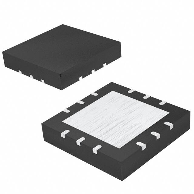
The OPA567 is available in a tiny 5mm x 5mm Quad
Flatpack No-lead (QFN) package and features an exposed
thermal pad that enhances thermal and electrical characteristics. It is small and easy to heat sink. The OPA567 is
specified for operation over the industrial temperature range,
–40°C to +85°C.
1, 12
–IN
The output of the OPA567 can be independently disabled
using the Enable pin. This feature saves power and protects
the load.
VO
6
9
4, 5
V–
NOTE: (1) Connect
for thermal protection.
RSET
FEATURES
PRODUCT
Same features as the OPA567, plus current
monitor output and paralleling ability in SO-20
PowerPAD™ package.
OPA569
ISET
Please be aware that an important notice concerning availability, standard warranty, and use in critical applications of
Texas Instruments semiconductor products and disclaimers thereto appears at the end of this data sheet.
PowerPAD is a trademark of Texas Instruments. All other trademarks are the property of their respective owners.
Copyright © 2005, Texas Instruments Incorporated
PRODUCTION DATA information is current as of publication date.
Products conform to specifications per the terms of Texas Instruments
standard warranty. Production processing does not necessarily include
testing of all parameters.
www.ti.com
�ABSOLUTE MAXIMUM RATINGS(1)
Supply Voltage ................................................................................. +7.5V
Output Current ............................................................... See SOA Curves
Signal Input Terminals (pins 8 and 9):
Voltage(2) ............................................... (V–) – 0.5V to (V+) + 0.5V
Current(2) ................................................................................ ±10mA
Output Short-Circuit(3) ........ Continuous when thermal protection enabled
Enable Pin (pin 11) ........................................ (V–) – 0.5V to (V–) + 7.5V
Current Limit Set, ILIMIT Pin (pin 6) ................ (V–) – 0.5V to (V+) + 0.5V
Operating Temperature .................................................. –55°C to +125°C
Storage Temperature ..................................................... –65°C to +150°C
Junction Temperature .................................................................... +150°C
ESD Rating:
Human Body Model ................................................................... 3kV
Charged Device Model .......................................................... 1500V
ELECTROSTATIC
DISCHARGE SENSITIVITY
This integrated circuit can be damaged by ESD. Texas
Instruments recommends that all integrated circuits be handled
with appropriate precautions. Failure to observe proper handling and installation procedures can cause damage.
ESD damage can range from subtle performance degradation to complete device failure. Precision integrated circuits
may be more susceptible to damage because very small
parametric changes could cause the device not to meet its
published specifications.
NOTES: (1) Stresses above these ratings may cause permanent damage.
Exposure to absolute maximum conditions for extended periods may degrade device reliability. These are stress ratings only, and functional operation of the device at these or any other conditions beyond those specified is
not implied. (2) Input terminals are diode-clamped to the power-supply rails.
Input signals that can swing more than 0.5V beyond the supply rails should
be current limited to 10mA or less. (3) Short-circuit to ground.
For the most current package and ordering information, see
the Package Option Addendum located at the end of this
data sheet.
PIN CONFIGURATION
PIN DESCRIPTIONS
3
V–
4
VO
2
TFLAG
10
9
+IN
8
–IN
7
IFLAG
PIN #
NAME
1, 12
V+
Positive Power-Supply Voltage
2, 3
VO
Output
4, 5
V–
Negative Power-Supply Voltage
6
ISET
Current Limit Set Pin(1)
7
IFLAG
Current Limit Flag—Indicates when part is in
current limit (active LOW).
DESCRIPTION
8
–IN
Inverting Input
9
+IN
Noninverting Input
10
TFLAG
11
ENABLE
6
2
ISET
VO
Metal
heat sink
(located
on bottom)
5
1
V–
V+
QFN
11
12
V+
Enable
Top View
PACKAGE/ORDERING INFORMATION
Thermal Flag—Indicates thermal stress (active
LOW).
Enabled HIGH, shut down LOW.
NOTE: (1) This pin limits the output current. The limited value, ILIMIT, is
9800(ISET), where ISET is the current flowing through the ISET pin. This current
is programmed by the resistor RSET connected to V–.
OPA567
www.ti.com
SBOS287A
�ELECTRICAL CHARACTERISTICS: VS = +2.7V to +5.5V
Boldface limits apply over the specified temperature range, TA = –40°C to +85°C.
At TCASE = +25°C, RL = 1kΩ, and connected to VS /2, unless otherwise noted.
OPA567
PARAMETER
OFFSET VOLTAGE
Input Offset Voltage
vs Temperature
vs Power Supply
INPUT BIAS CURRENT
Input Bias Current
vs Temperature
Input Offset Current
NOISE
Input Voltage Noise Density, f = 1kHz
f = 0.1Hz to 10Hz
Current Noise Density, f = 1kHz
INPUT VOLTAGE RANGE
Common-Mode Voltage Range
Common-Mode Rejection Ratio
CONDITION
VOS
dVOS /dT
PSRR
MIN
IO = 0V, VS = +5V
TA = –40°C to +85°C
VS = +2.7V to +5.5V, VCM = (V–) +0.55V
IOS
in
FREQUENCY RESPONSE
Gain Bandwidth Product
Slew Rate
Full-Power Bandwidth(1)
Settling Time: ±0.1%
Total Harmonic Distortion + Noise(2)
OUTPUT
Voltage Output Swing from Rail
Maximum Continuous Current Output: dc (4)
Capacitive Load Drive (5)
Closed-Loop Output Impedance(6)
AOL
GBW
SR
Linear Operation
VS = +5V, –0.1V < VCM < 3.2V
VS = +5V, –0.1V < VCM < 5.1V
(V–) – 0.1
80
60
0.2V < VO < 4.8V, RL = 1kΩ, VS = +5V
0.3V < VO < 4.7V, RL = 1.15Ω, VS = +5V
100
G = +1, VO = 4.0V Step
G = –1, VO = 4.0V Step
THD+N
VO
CLOAD
RO
RL = 1kΩ, AOL > 100dB
IO = ±2A, VS = +5V, AOL > 80dB (3)
(V–) + 0.2
(V–) + 0.3
ENABLE/SHUTDOWN INPUT
Enable Pin Bias Current
HIGH (Output enabled)
LOW (Output disabled)
Output Disable Time
Output Enable Time
Externally Adjustable
ILIMIT = 1A
ILIMIT = 1A
VSD
VSD
±0.5
±2
12
60
mV
µV/°C
µV/V
±1
(doubles every 10°C)
±2
±10
pA
±10
pA
VSD = 0V
Pin Open or Forced HIGH
Pin Forced LOW
RL = 1Ω
RL = 1Ω
nV/√Hz
µVPP
fA/√Hz
100
80
(V+) + 0.1
V
dB
dB
1013 || 4.5
1013 || 9
Ω || pF
Ω || pF
126
90
dB
dB
1.2
1.2
See Typical Characteristics
5
See Typical Characteristics
MHz
V/µs
(VS) ± 0.02
(VS) ± 0.2
µs
(V+) – 0.2
(V+) – 0.3
2.4
V
V
A
See Typical Characteristics
0.1
0.44
45
12M || 570
Ω
Ω
Ω
Ω || pF
±0.2 to ±2.2
ILIMIT = ISET • 9800
RSET = 9800 (1.18V/ILIMIT)
±3
±10
±3
±15
(V–) + 1.05
(V–) + 1.18
(V–) + 1.3
A
A
Ω
%
%
V
0.2
µA
V
V
µs
µs
G = 1, dc
G = 1, f = 10kHz
G = 1, f = 1.2MHz
Output Disabled Output Impedance
CURRENT LIMIT (ISET Pin)
Output Current Limit (7)
Current Limit Equation(8)
RSET Equation
Current Limit Tolerance (8), Positive
Negative
VSET Tolerance (9)
UNITS
12
8
0.6
en
INPUT IMPEDANCE
Differential
Common-Mode
OPEN-LOOP GAIN
Open-Loop Voltage Gain
MAX
±1.3
IB
VCM
CMRR
TYP
(V–) + 2.5
(V–) + 0.8
0.5
15
NOTES:
(1) See typical characteristic, Maximum Output Voltage vs Frequency.
(2) See typical characteristic, Total Harmonic Distortion + Noise vs Frequency.
(3) Swing to the rail is measured in final test. Under those conditions, the AOL is derived from characterization.
(4) See Safe Operating Area (SOA) plots.
(5) See typical characteristic, Overshoot vs Load Capacitance.
(6) See the Typical Characteristics section. Higher frequency output impedance can affect frequency stability.
(7) External current limit setting resistor is required; see Figure 1.
(8) ILIMIT is the value of the desired current limit and is equal to 9800(ISET), where ISET is the current through the ISET pin. ILIMIT tolerance is proportional to the ratio of
ILIMIT/ISET. Errors from this parameter can be calibrated out—see the Applications Information section.
(9) VSET is a voltage reference that equals the difference between the voltage of the ISET pin and V–, and is referenced to the negative rail. Errors from this parameter
can be calibrated out—see the Applications Information section.
OPA567
SBOS287A
www.ti.com
3
�ELECTRICAL CHARACTERISTICS: VS = +2.7V to +5.5V (Cont.)
Boldface limits apply over the specified temperature range, TA = –40°C to +85°C.
At TCASE = +25°C, RL = 1kΩ, and connected to VS /2, unless otherwise noted.
OPA567
PARAMETER
CONDITION
MIN
THERMAL FLAG PIN (TFLAG)
Junction Temperature:
TJ
Alarm (thermal status pin Low)
Return to normal operation (Thermal Flag pin High)
Thermal Flag Pin Voltage
During normal operation
During thermal overstress
TFLAG pin sourcing 25µA
TFLAG pin sinking 25µA
(V+) – 0.8V
CURRENT LIMIT FLAG PIN (IFLAG)
Current Limit Flag Pin Voltage
During normal operation
During current limit
IFLAG pin sourcing 25µA
IFLAG pin sinking 25µA
(V+) – 0.8V
POWER SUPPLY
Specified Voltage Range
Operating Voltage Range
Quiescent Current(10)
IQ
IO = 0, ILIMIT = 200mA, VS = 5V
IO = 0, ILIMIT = 2A, VS = 5V
IO = 0, VSD = 0.8V, VS = 5V
Junction Temperature
Junction Temperature
θJC
θJA
MAX
UNITS
°C
°C
+147
+130
V+
V–
(V–) + 0.8
V
V
V+
V–
(V–) + 0.8
V
V
+2.7
+2.5
VS
Quiescent Current in Shutdown Mode
TEMPERATURE RANGE
Specified Range
Operating Range
Storage Range
Thermal Resistance: Junction-to-Case
Junction-to-Ambient
Thermal overstress
Normal operation
TYP
+3.4
+9
+0.01
–40
–55
–65
6
38
+5.5
+5.5
+6
+11
V
V
mA
mA
mA
+85
+125
+150
°C
°C
°C
°C/W
°C/W
NOTES: (10) Quiescent current is a function of the current limit setting. See Adjustable Current Limit and Current Limit Flag Pin in the Applications Information section.
4
OPA567
www.ti.com
SBOS287A
�TYPICAL CHARACTERISTICS
At TA = +25°C, VS = +5V, unless otherwise noted.
POWER-SUPPLY AND COMMON-MODE
REJECTION RATIO vs FREQUENCY
0
160
–20
140
–40
120
–60
100
–80
80
–100
60
–120
40
–140
20
–160
0
–180
CMRR
100
0.1
1
10
100
1k
10k
100k
1M
80
60
40
0
1
10M
10
100
1k
Frequency (Hz)
OUTPUT SWING TO POSITIVE RAIL
vs SUPPLY VOLTAGE
OUTPUT SWING TO NEGATIVE RAIL
vs SUPPLY VOLTAGE
300
250
250
Swing to Rail (mV)
IOUT = 2A
150
IOUT = 1A
100
IOUT = 200mA
50
100k
IOUT = –2A
200
150
IOUT = –1A
100
50
IOUT = –200mA
0
0
2.7
3.0
3.5
4.0
4.5
5.0
5.5
2.7
3.0
3.5
4.0
4.5
5.0
Supply Voltage (V)
Supply Voltage (V)
OUTPUT SWING TO POSITIVE RAIL
vs TEMPERATURE
OUTPUT SWING TO NEGATIVE RAIL
vs TEMPERATURE
300
5.5
300
250
250
IO = 2A
IO = 2A
Swing to Rail (mV)
Swing to Rail (mV)
10k
Frequency (Hz)
300
200
PSRR
20
–200
–20
Swing to Rail (mV)
120
PSRR and CMRR (dB)
180
Phase (°)
AOL (dB)
OPEN-LOOP GAIN AND PHASE vs FREQUENCY
200
150
IO = 1A
100
150
IO = 1A
100
VS = 5V, IO = 200mA
VS = 2.7V, IO = 200mA
50
200
50
VS = 5V, IO = 200mA
0
VS = 2.7V, IO = 200mA
0
–55
–35
–15
5
25
45
65
85
–55
Temperature (°C)
–15
5
25
45
65
85
Temperature (°C)
OPA567
SBOS287A
–35
www.ti.com
5
�TYPICAL CHARACTERISTICS (Cont.)
At TA = +25°C, VS = +5V, unless otherwise noted.
INPUT VOLTAGE NOISE SPECTRAL DENSITY
vs FREQUENCY
0.1Hz TO 10Hz INPUT VOLTAGE NOISE
Input Voltage Noise (nV√Hz)
1000
1µV/div
100
10
1
10
100
1k
10k
1s/div
100k
Frequency (Hz)
TOTAL HARMONIC DISTORTION+NOISE
vs FREQUENCY
MAXIMUM OUTPUT VOLTAGE vs FREQUENCY
10
6
VS = 5V
RL = 1kΩ
1
4
RL = 1Ω
3
RL = 1kΩ
RL = 2Ω
THD+N (%)
Output Voltage (VPP)
5
0.1
RL = 8Ω
2
0.01
VS = 2.7V
1
RL = 1kΩ
RL = 1Ω
0.001
0
100
1k
10k
100k
20
1M
100
1k
10k 20k
Frequency (Hz)
Frequency (Hz)
QUIESCENT CURRENT vs TEMPERATURE
QUIESCENT CURRENT vs SUPPLY VOLTAGE
10
10
8
Quiescent Current (mA)
Quiescent Current (mA)
Current Limit = 2A
Current Limit = 1A
6
Current Limit = 200mA
4
2
IQ (ILIMIT = 2A)
6
4
IQ (ILIMIT = 200mA)
2
0
0
2.7
3.0
3.5
4.0
4.5
5.0
–55
5.5
–35
–15
5
25
45
65
85
105
125
Temperature (°C)
Supply Voltage (V)
6
8
OPA567
www.ti.com
SBOS287A
�TYPICAL CHARACTERISTICS (Cont.)
At TA = +25°C, VS = +5V, unless otherwise noted.
SHUTDOWN CURRENT vs TEMPERATURE
12
10
10
Shutdown Current (µA)
Shutdown Current (µA)
SHUTDOWN CURRENT vs SUPPLY VOLTAGE
12
8
ILIMIT = 200mA, 1A, and 2A
6
4
2
8
6
4
2
0
0
2.7
3.0
3.5
4.0
4.5
5.0
5.5
–55
–35
–15
5
Supply Voltage (V)
105
125
10000
8
1000
Input Bias Current (pA)
Quiescent Current (mA)
85
INPUT BIAS CURRENT vs TEMPERATURE
QUIESCENT CURRENT vs CURRENT LIMIT SETTING
10
6
4
2
100
10
1
0.1
0.01
0
0
0.5
1.0
1.5
2.0
2.5
–55
–35
–15
5
Current Limit Setting (A)
1.8
1.8
1.6
1.6
1.4
1.4
Slew Rate (V/µs)
2.0
SR–
1.0
0.8
SR+
0.6
45
65
85
105
125
SLEW RATE vs TEMPERATURE
2.0
1.2
25
Temperature (°C)
SLEW RATE vs LOAD RESISTANCE
Slew Rate (V/µs)
25
45
65
Temperature (°C)
1.2
1.0
0.8
0.6
0.4
0.4
0.2
0.2
0
SR+
SR–
0
1
10
100
1000
Load Resistance (Ω)
–35
–15
5
25
45
65
85
105
125
Temperature (°C)
OPA567
SBOS287A
–55
www.ti.com
7
�TYPICAL CHARACTERISTICS (Cont.)
At TA = +25°C, VS = +5V, unless otherwise noted.
VOLTAGE ON ISET PIN vs SUPPLY VOLTAGE
VOLTAGE ON ISET PIN vs TEMPERATURE
1.25
1.20
Current Limit = 200mA
1.20
[VSET – (V–)]
[VSET – (V–)] (V)
1.19
1.18
Current Limit = 1A
1.15
Current Limit = 2A
1.10
1.17
1.05
1.16
–55
–35
–15
5
25
45
65
85
105
2.7
125
3.0
3.5
4.0
4.5
5.0
5.5
Supply Voltage (V)
Temperature (°C)
OFFSET VOLTAGE
PRODUCTION DISTRIBUTION
OFFSET VOLTAGE DRIFT
PRODUCTION DISTRIBUTION
–10
–9
–8
–7
–6
–5
–4
–3
–2
–1
0
1
2
3
4
5
6
7
8
9
10
VOS (mV)
Drift (µV/°C)
SMALL-SIGNAL STEP RESPONSE
(G = +1, RL = 1kΩ)
LARGE-SIGNAL STEP RESPONSE
(G = +1, RL = 1kΩ)
1V/div
50mV/div
–2.0
–1.8
–1.6
–1.4
–1.2
–1.0
–0.8
–0.6
–0.4
–0.2
0
0.2
0.4
0.6
0.8
1.0
1.2
1.4
1.6
1.8
2.0
Population
Population
Typical Production
Distribution of
Packaged Units.
10µs/div
8
20µs/div
OPA567
www.ti.com
SBOS287A
�TYPICAL CHARACTERISTICS (Cont.)
At TA = +25°C, VS = +5V, unless otherwise noted.
LARGE-SIGNAL STEP RESPONSE
(G = +1, RL = 10Ω)
1V/div
50mV/div
SMALL-SIGNAL STEP RESPONSE
(G = +1, RL = 10Ω)
20µs/div
SMALL-SIGNAL STEP RESPONSE
(G = +1, RL = 1Ω)
LARGE-SIGNAL STEP RESPONSE
(G = +1, RL = 1Ω)
1V/div
50mV/div
10µs/div
20µs/div
20µs/div
ENABLE
(10Ω Load)
ENABLE
(1Ω Load)
2V/div
2V/div
Enable/Disable 0.8 to 2.5V
Above Negative Supply
Output Driven to +2V
1V/div
1V/div
Output Driven to +2V
10µs/div
4µs/div
OPA567
SBOS287A
Enable/Disable 0.8 to 2.5V
Above Negative Supply
www.ti.com
9
�TYPICAL CHARACTERISTICS (Cont.)
At TA = +25°C, VS = +5V, unless otherwise noted.
DISABLE
(1Ω Load)
2V/div
2V/div
DISABLE
(10Ω Load)
Enable/Disable 0.8 to 2.5V
Above Negative Supply
Output Driven
to +2V
1V/div
200ns/div
POWER ON
(1Ω Load)
POWER OFF
(1Ω Load)
5V/div
200ns/div
Supply 5V to 0V
1V/div
Supply 0V to 5V
Output Driven to +2V
Output Driven to +2V
1ms/div
IN AND OUT OF CURRENT LIMIT TRANSIENT
(RL = 0.75Ω, Current Limit = 2A)
IN AND OUT OF CURRENT LIMIT TRANSIENT
(RL = 7.5Ω, Current Limit = 200mA)
VOUT
(2V/div)
1ms/div
Current Limit Flag
(5V/div)
Current Limit Flag
(5V/div)
VOUT
(2V/div)
1V/div
5V/div
1V/div
Output Driven to +2V
200µs/div
200µs/div
10
Enable/Disable 0.8 to 2.5V
Above Negative Supply
OPA567
www.ti.com
SBOS287A
�TYPICAL CHARACTERISTICS (Cont.)
At TA = +25°C, VS = +5V, unless otherwise noted.
NO PHASE INVERSION WITH INPUTS
LARGER THAN SUPPLY VOLTAGE
(G = +1, RL = 10Ω)
OVERLOAD RECOVERY
(G = +1)
1V/div
1V/div
VIN
VOUT
VOUT
VIN
40µs/div
1ms/div
CURRENT LIMIT ERROR vs TEMPERATURE
CURRENT LIMIT ERROR vs SUPPLY VOLTAGE
15
15
10
Current Limit Error (%)
Current Limit Error (%)
10
ILIMIT –
5
0
ILIMIT+
–5
5
0
ILIMIT+
–10
–10
–15
–15
2.7
3.0
3.5
4.0
4.5
5.0
–55
5.5
–35
–15
5
25
45
65
Supply Voltage (V)
Temperature (°C)
CURRENT LIMIT ERROR vs OUTPUT CURRENT
OVERSHOOT vs LOAD CAPACITANCE
(G = +1, RL = 1kΩ)
85
50
15
10
40
ILIMIT –
5
Overshoot (%)
Current Limit Error (%)
ILIMIT –
–5
0
ILIMIT+
–5
30
20
10
–10
–15
0
0.2
0.4
0.6
0.8
1.0
1.2
1.4
1.6
1.8
10
2.0
Output Current (A)
1k
10k
Load Capacitance (pF)
OPA567
SBOS287A
100
www.ti.com
11
�TYPICAL CHARACTERISTICS (Cont.)
At TA = +25°C, VS = +5V, unless otherwise noted.
CLOSED-LOOP OUTPUT IMPEDANCE
vs FREQUENCY
100
Output Impedance (Ω)
G=1
10
1
0.1
10k
12
100k
Frequency (Hz)
1M
2M
OPA567
www.ti.com
SBOS287A
�APPLICATIONS INFORMATION
R1
R2
BASIC CONFIGURATION
V+
Figure 1 shows the OPA567 connected as a basic noninverting amplifier. However, the OPA567 can be used in
virtually any op amp configuration. A current limit setting
resistor (RSET, in Figure 1) is essential to the OPA567
operation, and cannot be omitted.
47µF
0.1µF
1, 12
8
2, 3
Power-supply terminals should be bypassed with low series
impedance capacitors. Using larger tantalum and smaller
ceramic type capacitors in parallel is recommended. Powersupply wiring should have low series impedance.
OPA567
VIN
9
4, 5
47µF
11
0.1µF
The OPA567 operates with excellent performance from a
single (+2.7V to +5.5V) supply or from dual supplies. Power
supply voltages do not need to be equal as long as the total
voltage remains below 5.5V. Parameters that vary significantly with operating voltage are shown in the Typical
Characteristics section.
Setting the current limit
RSET (Ω)
ILIMIT (A)
23.2k
11.5k
7.68k
5.76k
0.5
1.0
1.5
2.0
47µF
NOTES: (1) RSET sets the current
limit value from 0.2A to 2.2A.
RSET can be a potentiometer to
easily adjust current limit and
calibrate out errors at the current
limit node. (2) Enable—pull Low
to disable output.
ADJUSTABLE CURRENT LIMIT AND CURRENT
LIMIT FLAG PIN
The OPA567 provides over-current protection to the load
through its accurate, user-adjustable current limit (pin 6). The
current limit value, ILIMIT, can be set from 0.2A to 2.2A by
controlling the current to the ISET pin. The current limit, ILIMIT,
will be 9800 • ISET, where ISET is the current through the ISET
pin. Setting the current limit requires no special power
resistors. The output current does not flow through this pin.
ISET
RSET(1)
Enable(2)
POWER SUPPLIES
VO
6
V–
FIGURE 1. Basic Connections.
the ISET pin and V–, the negative supply, according to the
formula:
ILIMIT = 9800 • (1.18V/RSET)
Alternatively, the output current limit can be set by applying
a voltage source in series with a resistance using the equation:
As illustrated in Figure 2, the simplest method of setting the
current limit is to connect a resistor or potentiometer between
ILIMIT = 9800 • [(1.18V – VADJUST)/RSET]
The voltage source must be referenced to V–.
8
8
2, 3
2, 3
1.18V
9
6 ISET
4, 5
1.18V
9
ILIMIT = 9800 (1.18V/RSET)
6 ISET
RSET
4, 5
ILIMIT = 9800 (1.18V – VADJUST)
RSET
VADJUST(1)
RPOT
V–
V–
(a) Resistor or Potentiometer Method
(b) Resistor/Voltage Source Method
Putting a set resistor in series with the potentiometer
will prevent potential short-circuit on pin.
NOTE: (1) This voltage source must be able to
sink the current from the ISET pin, which is ILIMIT/9800.
FIGURE 2. Setting the Current Limit—Resistor Method.
OPA567
SBOS287A
www.ti.com
13
�Current Limit Accuracy
ENABLE PIN—OUTPUT DISABLE
Internally separate circuits monitor the positive and negative
current limits. Each circuit output is compared to a single
internal reference that is set by the user with an external
resistor or a resistor/voltage source combination. The OPA567
employs a patented circuit technique to achieve an accurate
and stable current limit throughout the full output range. The
initial accuracy of the current limit is typically within 3%;
however, because of internal matching limitations, the error
can be as much as 15%. The variation of the current limit with
factors such as output current level, output voltage, and
temperature is shown in the Typical Characteristics section.
The Enable pin can disable the OPA567 within microseconds. When disabled, the amplifier draws less than 10µA and
its output enters a high-impedance state that allows multiplexing. It is important to note that when the amplifier is
disabled, the Thermal Flag pin (TFLAG) circuitry continues to
operate. This feature allows use of the TFLAG pin output to
implement thermal protection strategies. For more details,
please see the section on thermal protection.
When the accuracy of one current limit (sourcing or sinking)
is more important than the other, it is possible to set its
accuracy to better than 1% by adjusting the external resistor
or the applied voltage. The accuracy of the other current limit
will still be affected by internal matching.
Current Limit Flag Pin
The OPA567 features an IFLAG pin (pin 7) that can be
monitored to determine when the part is in current limit. The
output signal of the IFLAG pin is compatible to standard logic
in single-supply applications. The output signal is a CMOS
logic gate that switches from V+ to V– to indicate that the
amplifier is in current limit. The IFLAG pin can source and sink
up to 25µA. Additional parasitic capacitance between pins 6
and 7 can cause instability at the edge of the current limit.
Avoid routing these traces in parallel close to each other.
Quiescent Current Dependence on the
Current Limit Setting
The OPA567 is a low-power amplifier, with a typical 3.4mA
quiescent current (with the current limit configured for 200mA).
The quiescent current varies with the current limit setting—
it increases 0.5mA for each additional 200mA increase in
the current limit, as shown in Figure 3.
The OPA567 Enable pin has an internal pull-up circuit, so it
does not have to be connected to the positive supply for
normal operation. To disable the amplifier, the Enable pin
must be connected to no more than (V–) + 0.8V. To enable
the amplifier, either allow the Enable pin to float or connect
it to at least (V–) + 2.5V.
The Enable pin is referenced to the negative supply (V–).
Therefore, shutdown operation is slightly different in singlesupply and dual-supply applications.
In single-supply operation, V– typically equals common
ground; thus, the enable/disable logic signal and the OPA567
Enable pin are referenced to the same potential. In this
configuration, the logic level and the OPA567 Enable pin can
simply be tied together. Disabling the OPA567 occurs for
voltage levels of less than 0.8V. The OPA567 is enabled at
logic levels greater than 2.5V.
In dual-supply operation, the logic level is referenced to a
logic ground. However, the OPA567 Enable pin is still referenced to V–. To disable the OPA567, the voltage level of the
logic signal needs to be level-shifted. This level-shifting can
be done using an optocoupler, as shown in Figure 4.
Examples of output behavior during disabled and enabled
conditions with various load impedances are shown in the
typical characteristics section. Please note that this behavior
is a function of board layout, load impedances, and bypass
strategies. For sensitive loads, the use of a low-pass filter or
other protection strategy is recommended.
QUIESCENT CURRENT vs CURRENT LIMIT SETTING
V+
10
(a) +5V
(b) HCT or TTL In
Quiescent Current (mA)
1, 12
8
8
9
6
OPA567
11
(1)
2, 3
VO
Enable
4, 5
4
2
4N38
Optocoupler
0
0
0.5
1
1.5
2
V–
2.5
Current Limit Setting (A)
(a) HCT or
TTL In
FIGURE 3. Quiescent Current vs Current Limit Setting.
14
(b)
NOTE: (1) Optional—may be required
to limit leakage current of optocoupler
at high temperatures.
FIGURE 4. OPA567 Shutdown Configuration for Dual
Supplies.
OPA567
www.ti.com
SBOS287A
�ENSURING MICROCONTROLLER COMPATIBILITY
+V
Not all microcontrollers output the same logic state after
power-up or reset. 8051-type microcontrollers, for example,
output logic High levels on their ports while other models
power up with logic Low levels after reset.
1, 12
–In
In configuration (a) shown in Figure 4, the enable/disable
signal is applied on the cathode side of the photodiode within
the optocoupler. A logic High level causes the OPA567 to be
enabled, and a logic Low level disables the OPA567. In
configuration (b) of Figure 4, with the logic signal applied on
the anode side, a high level disables the OPA567 and a low
level enables the op amp.
OPA567
+In
2, 3
VO
9
6
ISET
4, 5
Output Protection Diode
RSET
RAIL-TO-RAIL OUTPUT RANGE
–V
The OPA567 has a class AB output stage with common
source transistors that are used to achieve rail-to-rail output
swing. It was designed to be able to swing closer to the rail
than other existing linear amplifiers, even with high output
current levels. A quick way to estimate the output swing with
various output current requirements is by using the equation:
VSWING [typical] = 0.1 • IO
Plots of the Output Swing vs Output Current, Supply Voltage,
and Temperature are provided in the Typical Characteristics
section.
RAIL-TO-RAIL INPUT RANGE
The input common-mode voltage range of the OPA567
extends 100mV beyond the supply rails. This is achieved by
a complementary input stage with an N-channel input differential pair in parallel with a P-channel differential pair. The
N-channel input pair is active for input voltages close to the
positive rail while the P-channel input pair is active for input
voltages close to the negative rail. The transition point is
typically at (V+) – 1.3V, and there is a small transition region
around the switching point where both transistors are on. It
is important to note that the two input pairs can have offsets
of different signs and magnitudes. Therefore, as the transition point is crossed, the offset of the amplifier changes. This
offset shift accounts for the reduced common-mode rejection
ratio over the full input common-mode range.
OUTPUT PROTECTION
Reactive and EMF-generating loads can return load current
to the amplifier, causing the output voltage to exceed the
power-supply voltage. This damaging condition can be
avoided with clamp diodes from the output terminal to the
power supplies, as shown in Figure 5. Schottky rectifier
diodes with a 3A or greater continuous rating are recommended.
FIGURE 5. Output Protection Diode.
THERMAL FLAG PIN
The OPA567 has thermal sensing circuitry that provides a
warning signal when the die temperature exceeds safe limits.
Unless the TFLAG pin is connected to the Enable pin, when
this flag is triggered, the part continues to operate even
though the junction temperature exceeds 150°C. This default
operation allows maximum usable operation in very harsh
conditions but degrades reliability. The TFLAG pin can be used
to provide for orderly system shutdown before failure occurs.
It can be also used to evaluate the thermal environment to
determine need for and appropriate design of a shutdown
mechanism.
The thermal flag output signal is from a CMOS logic gate that
switches from V+ to V– to indicate that the amplifier is in
thermal limit. This flag output pin can source and sink up to
25µA. The TFLAG pin is HIGH during normal operation. Power
dissipated in the amplifier will cause the junction temperature
to rise. When the junction temperature exceeds 150°C, the
TFLAG pin will go Low, and remain Low until the amplifier has
cooled to 130°C. Despite this hysteresis, with a method of
orderly shutdown, the TFLAG pin can cycle on and off, depending on load and signal conditions. This limits the dissipation of the amplifier but may have an undesirable effect on
the load.
It is possible to connect the TFLAG pin directly to the Enable
pin for automatic shutdown protection. When both thermal
shutdown and the amplifier enable/disable functions are
desired, the externally generated control signal and the TFLAG
pin outputs should be combined with an AND gate; see
Figure 6. The temperature protection was designed to protect against overload conditions. It was not intended to
replace proper heatsinking. Continuously running the OPA567
in and out of thermal shutdown will degrade reliability.
OPA567
SBOS287A
Output Protection Diode
8
www.ti.com
15
�SAFE OPERATING AREA
(TA = 25°C)
On
10
AND
Output Current (A)
Disable
TFLAG Pin
Enable Pin
10
8
9
11
OPA567
2, 3
Thermal pad soldered
to 2 oz. copper pad,
with 500lfm airflow.
1
Thermal pad soldered
to 2 oz. copper pad,
without forced air.
0.1
0
FIGURE 6. Enable/Shutdown Control Using TFLAG Pin and
External Control Signal.
1
2
3
4
5
6
VS – VOUT (V)
FIGURE 7. Safe Operating Area at Room Temperature.
Any tendency to activate the thermal protection circuit indicates excessive power dissipation or an inadequate heat
sink. For reliable, long term, continuous operation, the junction temperature should be limited to 125°C maximum. To
estimate the margin of safety in a complete design (including
heat sink), increase the ambient temperature until the thermal protection is triggered. Use worst-case loading and
signal conditions. For good, long-term reliability, thermal
protection should trigger more than 25°C above the maximum expected ambient conditions of your application. This
produces a junction temperature of 125°C at the maximum
expected ambient condition.
Fast transients of large output current swings (for example,
switching quickly from sourcing 2A to sinking 2A) may cause
a glitch on the TFLAG pin. When switching large currents is
expected, the use of extra bypass between the supplies or a
low-pass filter on the TFLAG pin is recommended.
POWER DISSIPATION AND
SAFE OPERATING AREA
Power dissipation depends on power supply, signal, and load
conditions. It is dominated by the power dissipation of the
output transistors. For DC signals, power dissipation is equal
to the product of output current, IOUT and the output voltage
across the conducting output transistor (VS – VOUT). Dissipation with AC signals is lower. Application Bulletin SBOA022
explains how to calculate or measure power dissipation with
unusual signals and loads and can be found at the TI web
site (www.ti.com).
Output short-circuits are particularly demanding for the amplifier because the full supply voltage is seen across the
conducting transistor. It is very important to note that the
temperature protection will not shut the part down in overtemperature conditions, unless the TFLAG pin is connected to
the Enable pin; see the section on Thermal Flag.
Figure 7 shows the safe operating area at room temperature
with various heatsinking efforts. Note that the safe output
current decreases as (VS – VOUT) increases. Figure 8 shows
the safe operating area at various temperatures with the
metal heatsink being soldered to a 2oz copper pad.
16
SAFE OPERATING AREA
Thermal Pad Soldered, Various TA
10
Output Current (A)
TA = –40°C
TA = 0°C
1
TA = +85°C
TA = +25°C
0.1
0
1
2
3
4
5
6
VS – VOUT (V)
FIGURE 8. Safe Operating Area at Various Ambient Temperatures. Metal heat sink soldered to a 2oz copper pad.
The power that can be safely dissipated in the package is
related to the ambient temperature and the heatsink design.
The QFN package was specifically designed to provide
excellent power dissipation, but board layout greatly influences the heat dissipation of the package. Refer to
the QFN Package section for further details.
The OPA567 has a junction-to-ambient thermal resistance
(θJA) value of 38°C/W when soldered to a 2oz copper plane.
This value can be further decreased by the addition of forced
air. See Figure 9 for the junction-to-ambient thermal resistance of the QFN-12 package.
Junction temperature should be kept below 125°C for reliable
operation. The junction temperature can be calculated by:
TJ = TA + PDθJA
where θJA = θJC + θCA
TJ = Junction Temperature (°C)
TA = Ambient Temperature (°C)
PD = Power Dissipated (W)
θJA = Junction-to-Ambient Thermal Resistance
θJC = Junction-to-Case Thermal Resistance
θCA = Case-to-Air Thermal Resistance
OPA567
www.ti.com
SBOS287A
�θJA
The part is soldered to a 2 oz copper pad under the
exposed pad.
38
Soldered to copper pad with forced airflow (150lfm).
36
Soldered to copper pad with forced airflow (250lfm).
35
Soldered to copper pad with forced airflow (500lfm).
34
THERMAL RESISTANCE
vs NUMBER OF THERMAL VIAS
100
Thermal Resistance, θJA (°C/W)
HEATSINKING METHOD
FIGURE 9. Junction-to-Ambient Thermal Resistance with
Various Heatsinking Efforts.
The Maximum Power Dissipation vs Temperature for the
heatsinking methods referenced in Figure 9 is shown in
Figure 10.
90
80
70
60
50
40
30
20
10
0
0
1
2
3
4
5
6
Number of Thermal Vias
FIGURE 11. Thermal Resistance vs Number of Thermal Vias.
MAXIMUM POWER DISSIPATION IN PACKAGE
vs TEMPERATURE
FEEDBACK CAPACITOR IMPROVES RESPONSE
6
TJ = 150°C
Power Dissipated (W)
For optimum settling time and stability with higher impedance
feedback networks (RF > 50kΩ), it may be necessary to add
a feedback capacitor across the feedback resistor, RF, as
shown in Figure 12. This capacitor compensates for the zero
created by the feedback network impedance and the input
capacitance of the OPA567 (and any parasitic layout capacitance). The effect becomes more significant with higher
impedance networks.
Thermal pad soldered
to 2oz. copper pad,
with 500lfm airlow.
5
4
3
Thermal pad soldered
to 2oz. copper pad,
without forced air.
2
The size of the capacitor needed is estimated using the
equation:
1
RIN • CIN = RF • CF
0
–75
–50
–25
0
25
50
75
100
125
where CIN is the sum of the input capacitance of the OPA567
plus the parasitic layout capacitance.
Temperature (°C)
FIGURE 10. Maximum Power Dissipation vs Temperature.
CF
To appropriately determine required heatsink area, required
power dissipation should be calculated and the relationship
between power dissipation and thermal resistance should be
considered to minimize shutdown conditions and allow for
proper long-term operation (junction temperature of 125°C).
Once the heatsink area has been selected, worst-case load
conditions should be tested to ensure proper thermal protection.
RIN
RF
VIN
V+
1, 12
8
CIN
2, 3
RIN • CIN = RF • CF
For applications with limited board size, refer to Figure 11 for
the approximate thermal resistance relative to the number of
thermal vias. The QFN-12 package is well suited for continuous power levels, as shown in Figure 10. Higher power levels
may be achieved in applications with a low on/off duty cycle.
VOUT
OPA567
9
CL
CIN
4, 5
V–
Where CIN is equal to the OPA567 input
capacitance (approximately 9pF) plus any
parasitic layout capacitance.
FIGURE 12. Feedback Capacitor for Use with Higher Impedance Networks.
OPA567
SBOS287A
www.ti.com
17
�QFN THERMALLY ENHANCED PACKAGE
The OPA567 uses the QFN-12 package, a thermallyenhanced package designed to eliminate the use of bulky
heat sinks and slugs traditionally used in thermal packages.
This package can be easily mounted using standard printed
circuit board (PCB) assembly techniques. See QFN/SON
PCB Attachment Application Note (SLUA271) located at
www.ti.com.
The thermal resistance junction-to-ambient (RθJA) of the QFN
package depends on the PCB layout. Using thermal vias and
wide PCB traces improve thermal resistance. The thermal
pad must be soldered to the PCB. The thermal pad should
either be left floating or connected to V–.
LAYOUT GUIDELINES
The OPA567 is a power amplifier that requires proper layout
for best performance. An example layout is appended to the
end of this datasheet. Refinements to this layout may be
required based on assembly process requirements.
power- supply leads. The wire length should be less than 8
inches.
Proper power-supply bypassing with low ESR capacitors is
essential to achieve good performance. A parallel combination of 100nF ceramic and 47µF tantalum bypass capacitors
will provide low impedance over a wide frequency range.
Bypass capacitors should be placed as close as practical to
the power-supply pins of the OPA567.
PCB traces conducting high currents, such as from output to
load or from the power-supply connector to the power-supply
pins of the OPA567 should be kept as wide and short as
possible. This practice will keep inductance low and resistive
losses to a minimum.
The nine holes in the landing pattern for the OPA567 are for
the thermal vias that connect the thermal pad of the OPA567
to the heatsink area on the PCB. All traces conducting high
currents are very wide for lowest inductance and minimal
resistive losses.
Keep power-supply leads as short as possible. This practice
will keep inductance low and resistive losses at a minimum.
A minimum of 18 gauge wire thickness is recommended for
18
OPA567
www.ti.com
SBOS287A
�APPLICATION CIRCUITS
R2
4.99kΩ
fO = 10kHz
0.0033µF
+1V
0V
R1
49.9kΩ
0mA
–100mA
1, 12
8
VIN
9
OPA567
(1)
R3
49.9kΩ
2, 3 VO
6
RSET
RSHUNT
1Ω
4, 5
IO
0V
–2.5V
Luxeon Star-0
High-Power LED
–5V
4.99kΩ
Feedback for Constant Current,
1V Input per 100mA Output as Shown.
NOTE: (1) Bypass as recommended.
FIGURE 13. Grounded Anode LED Driver.
1kΩ
1kΩ
5V
5V
1, 12
1, 12
(1)
8
VIN
9
OPA567
6
8
TEC
2, 3
2, 3
ISET
+
4, 5
RSET
VTEC
(1)
OPA567
ISET
3
–
Heat/Cool
9
VSET
4, 5
RSET
VTEC = 2 (VIN – VSET)
NOTE: (1) Bypass as recommended.
FIGURE 14. Bridge-Tied Load Driver.
NOTE: Total Supply Must
be < 5.5V Cooling/Heating.
+3.3V
1, 12
(1)
8
VIN
9
IL
2, 3
OPA567
6 ISET
4, 5
TEC
RSET
–1.2V
NOTE: (1) Bypass as recommended.
FIGURE 15. Single Power Amplifier Driving Bidirectional Current through a TEC using Asymmetrical Bipolar Power Supplies.
OPA567
SBOS287A
www.ti.com
19
�PACKAGE OPTION ADDENDUM
www.ti.com
14-Oct-2022
PACKAGING INFORMATION
Orderable Device
Status
(1)
Package Type Package Pins Package
Drawing
Qty
Eco Plan
(2)
Lead finish/
Ball material
MSL Peak Temp
Op Temp (°C)
Device Marking
(3)
Samples
(4/5)
(6)
OPA567AIRHGR
ACTIVE
VQFN
RHG
12
2500
RoHS & Green
NIPDAU
Level-2-260C-1 YEAR
-55 to 125
OPA
567AI
Samples
OPA567AIRHGT
ACTIVE
VQFN
RHG
12
250
RoHS & Green
NIPDAU
Level-2-260C-1 YEAR
-55 to 125
OPA
567AI
Samples
(1)
The marketing status values are defined as follows:
ACTIVE: Product device recommended for new designs.
LIFEBUY: TI has announced that the device will be discontinued, and a lifetime-buy period is in effect.
NRND: Not recommended for new designs. Device is in production to support existing customers, but TI does not recommend using this part in a new design.
PREVIEW: Device has been announced but is not in production. Samples may or may not be available.
OBSOLETE: TI has discontinued the production of the device.
(2)
RoHS: TI defines "RoHS" to mean semiconductor products that are compliant with the current EU RoHS requirements for all 10 RoHS substances, including the requirement that RoHS substance
do not exceed 0.1% by weight in homogeneous materials. Where designed to be soldered at high temperatures, "RoHS" products are suitable for use in specified lead-free processes. TI may
reference these types of products as "Pb-Free".
RoHS Exempt: TI defines "RoHS Exempt" to mean products that contain lead but are compliant with EU RoHS pursuant to a specific EU RoHS exemption.
Green: TI defines "Green" to mean the content of Chlorine (Cl) and Bromine (Br) based flame retardants meet JS709B low halogen requirements of


 工商网监
湘ICP备2023018690号
工商网监
湘ICP备2023018690号
