5/8/12
TPS40170 – 5V@2.1A (x2) Test Results Rev. A
TPS40170 + TPS2511 – 5V@2.1A (x2)
Universal USB Car Charger
PMP7390_REVA
5/8/12
The tests performed were as follows:
A. TPS40170 – 5V@2.1A (x2)
1. Board Photo
2. Thermal Image
3. Turn-On (No Load)
4. Output Voltage Ripple
5. Transient Response
6. Switching Behavior
7. Efficiency
8. Load Regulation
9. Loop Response
Page 1 of 8
Power Management Solutions
�5/8/12
TPS40170 – 5V@2.1A (x2) Test Results Rev. A
1
Board Photo
The photo below shows the front and back of the PMP7390 board.
2
Thermal Image
The thermal images of the board are taken with 2A load. The input voltage is 12V.
Page 2 of 8
Power Management Solutions
�5/8/12
TPS40170 – 5V@2.1A (x2) Test Results Rev. A
3
Turn-On – (TPS40170 : 5V@0A)
The photo below shows the startup waveforms. The output is not loaded. The timebase is set to 10ms/Division. The input
voltage is 12V.
Channel 1 – Yellow : 5V Output After the USB Switch – (2V/Division)
Channel 2 – Pink : Input Voltage – (5V/Division)
4
Output Voltage Ripple – (TPS40170 : 5V@2.1A (x2))
The photo below shows the output voltage ripple. The input voltage is 12V. The timebase is set to 2us/division.
Channel 3 – Blue : Output Voltage Ripple – (20mV/Division; AC Coupled)
Channel 4 – Green : Output Current – (2A/Division)
No Load, Measured Before the USB Switch
Page 3 of 8
4.2A Load, Measured Before the USB Switch
Power Management Solutions
�5/8/12
TPS40170 – 5V@2.1A (x2) Test Results Rev. A
2.1A Load, Measured After the USB Switch at the End of an iPhone Cable
5
Transient Response – (TPS40170 : 5V@2.1A (x2))
The transient response of the converter is shown in the figure below. The input voltage is 12V. The current is pulsed from
0.1A to 1A, 1A to 2A and 0.1A to 2A. The timebase is set to 2ms/Division. The cable droop compensation is set to
increase the output voltage 200mV at ~1.3A
Channel 2 – Pink : Output Voltage Before the USB Switch – (200mV/Division; AC Coupled)
Channel 3 – Blue : Output Voltage After the USB Switch – (200mV/Division; AC Coupled)
Channel 4 – Green : Output Current – (1A/Division)
0.1A to 1A (no cable droop compensation)
Page 4 of 8
1A to 2A
Power Management Solutions
�5/8/12
TPS40170 – 5V@2.1A (x2) Test Results Rev. A
0.1 to 2A
6
Switching Behavior – (TPS40170 : 5V@2.1A (x2))
The switching behavior of the converter is shown in the figure below. The input voltage is set to 12V, the output current is
set to 4.2A. The timebase is set to 2us/Divison.
Channel 1 – Yellow : Switch Node – (5V/Division
Channel 3 – Blue : Output Voltage Before the USB Switch – (20mV/Division; AC Coupled)
Channel 4 – Green : Inductor Ripple Current – (1A/Division)
No Load
Page 5 of 8
4.2A Load
Power Management Solutions
�5/8/12
TPS40170 – 5V@2.1A (x2) Test Results Rev. A
7
Efficiency – (TPS40170 : 5V@2.1A (x2))
The efficiency of the converter is shown in the figures below.
Efficiency vs. Load Current
100%
95%
Efficiency
90%
85%
80%
75%
70%
65%
60%
0.1
0.6
1.1
1.6
2.1
2.6
3.1
3.6
4.1
Load Current (A)
9Vin
12Vin
20Vin
30Vin
40Vin
Efficiency Before the USB Switch
Efficiency vs. Load Current
100%
95%
Efficiency
90%
85%
80%
75%
70%
65%
60%
0.1
0.3
0.5
0.7
0.9
1.1
1.3
1.5
1.7
1.9
2.1
Load Current (A)
9Vin
12Vin
20Vin
30Vin
40Vin
Efficiency After the USB Switch
Page 6 of 8
Power Management Solutions
�5/8/12
TPS40170 – 5V@2.1A (x2) Test Results Rev. A
8
Load Regulation – (TPS40170 : 5V@2.1A (x2))
The load regulation of the converter is shown in the figure below.
Output Voltage (V)
Output Voltage vs. Load Current
5.25
5.20
5.15
5.10
5.05
5.00
4.95
4.90
4.85
4.80
4.75
0.1
0.6
1.1
1.6
2.1
2.6
3.1
3.6
4.1
Load Current (A)
9Vin
12Vin
20Vin
30Vin
40Vin
Output Load Regulation Before the USB Switch
Output Voltage vs. Load Current
Output Voltage (V)
5.25
5.20
5.15
5.10
5.05
5.00
4.95
4.90
4.85
4.80
4.75
0.1
0.3
0.5
0.7
0.9
1.1
1.3
1.5
1.7
1.9
2.1
Load Current (A)
9Vin
12Vin
20Vin
30Vin
40Vin
Output Load Regulation After the USB Switch
Page 7 of 8
Power Management Solutions
�5/8/12
TPS40170 – 5V@2.1A (x2) Test Results Rev. A
9
Loop Response – (TPS40170 : 5V@2.1A (x2))
The loop response of the converter is shown in the image below. The input is 12V, the outputs are fully loaded.
Page 8 of 8
Power Management Solutions
�IMPORTANT NOTICE AND DISCLAIMER
TI PROVIDES TECHNICAL AND RELIABILITY DATA (INCLUDING DATASHEETS), DESIGN RESOURCES (INCLUDING REFERENCE
DESIGNS), APPLICATION OR OTHER DESIGN ADVICE, WEB TOOLS, SAFETY INFORMATION, AND OTHER RESOURCES “AS IS”
AND WITH ALL FAULTS, AND DISCLAIMS ALL WARRANTIES, EXPRESS AND IMPLIED, INCLUDING WITHOUT LIMITATION ANY
IMPLIED WARRANTIES OF MERCHANTABILITY, FITNESS FOR A PARTICULAR PURPOSE OR NON-INFRINGEMENT OF THIRD
PARTY INTELLECTUAL PROPERTY RIGHTS.
These resources are intended for skilled developers designing with TI products. You are solely responsible for (1) selecting the appropriate
TI products for your application, (2) designing, validating and testing your application, and (3) ensuring your application meets applicable
standards, and any other safety, security, or other requirements. These resources are subject to change without notice. TI grants you
permission to use these resources only for development of an application that uses the TI products described in the resource. Other
reproduction and display of these resources is prohibited. No license is granted to any other TI intellectual property right or to any third party
intellectual property right. TI disclaims responsibility for, and you will fully indemnify TI and its representatives against, any claims, damages,
costs, losses, and liabilities arising out of your use of these resources.
TI’s products are provided subject to TI’s Terms of Sale (https:www.ti.com/legal/termsofsale.html) or other applicable terms available either
on ti.com or provided in conjunction with such TI products. TI’s provision of these resources does not expand or otherwise alter TI’s
applicable warranties or warranty disclaimers for TI products.IMPORTANT NOTICE
Mailing Address: Texas Instruments, Post Office Box 655303, Dallas, Texas 75265
Copyright © 2021, Texas Instruments Incorporated
�
很抱歉,暂时无法提供与“PMP7390”相匹配的价格&库存,您可以联系我们找货
免费人工找货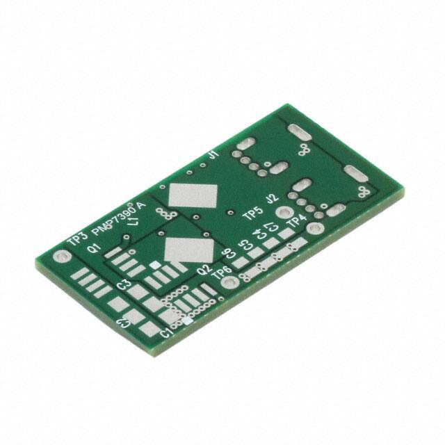


 工商网监
湘ICP备2023018690号
工商网监
湘ICP备2023018690号
