PTH03060Y
PTH05060Y, PTH12060Y
www.ti.com
SLTS222A – MARCH 2004 – REVISED OCTOBER 2005
10-A NON-ISOLATED DDR/QDR
MEMORY BUS TERMINATION MODULES
FEATURES
•
•
•
•
•
•
•
•
•
VTT Bus Termination Output
(Output Tracks the System VREF)
10 A Output Current
3.3-V, 5-V or 12-V Input Voltage
DDR and QDR Compatible
On/Off Inhibit (for VTT Standby)
Undervoltage Lockout
Operating Temperature: –40°C to 85°C
Efficiencies up to 91%
Output Overcurrent Protection (Non-Latching,
Auto-Reset)
•
•
•
57 W/in3 Power Density
Safety Agency Approvals:
UL/cUL60950, EN60950, VDE
Point-of-Load Alliance (POLA™) Compatible
NOMINAL SIZE
1 in. x 0.62 in
(25,4 mm x 15,75 mm)
DESCRIPTION
The PTHxx060Y are a series of ready-to-use switching regulator modules from Texas Instruments designed
specifically for bus termination in DDR and QDR memory applications. Operating from either a 3.3-V, 5-V or 12-V
input, the modules generate a VTT output that will source or sink up to 10 A of current to accurately track their
VREF input. VTT is the required bus termination supply voltage, and VREF is the reference voltage for the memory
and chipset bus receiver comparators. VREF is usually set to half the VDDQ power supply voltage.
Both the PTHxx060Y series employs an actively switched synchronous rectifier output to provide state-of-the-art
stepdown switching conversion. The products are small in size (1 in × 0.62 in), and are an ideal choice where
space, performance, and high efficiency are desired, along with the convenience of a ready-to-use module.
Operating features include an on/off inhibit and output over-current protection (source mode only). The on/off
inhibit feature allows the VTT bus to be turned off to save power in a standby mode of operation. To ensure tight
load regulation, an output remote sense is also provided. Package options include both throughhole and surface
mount configurations.
STANDARD APPLICATION
VIN
VREF
VDDQ
1k
1%
1
10
9
8
VTT
7
PTHxx060Y
(Top View)
1k
1%
2
Con
hf−Ceramic
6
3
4
5
Standby
Q1
BSS138
(Optional)
GND
Co1
Low−ESR
(Required)
Co2
Ceramic
(Optional)
VTT Termination Island
CIN
(Required)
SSTL−2
Bus
CIN = Required Capacitor; 330µF (3.3 ± 5 V Input), 560 µF (12 V Input).
Co1 = Required Low-ESR Electrolyitic Capacitor; 470 µF (3.3 ± 5 V Input), 940 µF (12 V Input).
Co2 = Ceramic Capacitance for Optimum Response to a 3 A (+ 1.5 A) Load Transient; 200 µF (3.3 ± 5 V Input), 400 µF (12 V Input).
Con = Distributed hf-Ceramic Decoupling Capacitors for VTT bus; as Recommended for DDR Memory Applications.
Please be aware that an important notice concerning availability, standard warranty, and use in critical applications of Texas
Instruments semiconductor products and disclaimers thereto appears at the end of this data sheet.
POLA is a trademark of Texas Instruments.
PRODUCTION DATA information is current as of publication date.
Products conform to specifications per the terms of the Texas
Instruments standard warranty. Production processing does not
necessarily include testing of all parameters.
Copyright © 2004–2005, Texas Instruments Incorporated
�PTH03060Y
PTH05060Y, PTH12060Y
www.ti.com
SLTS222A – MARCH 2004 – REVISED OCTOBER 2005
ORDERING INFORMATION
PTHXX060Y (Base Part Number)
Input Voltage
Part Number
3.3 V
5V
12 V
(1)
(2)
(3)
(4)
(1)
DESCRIPTION
Pb – free and
RoHS
(3)
Mechanical Package
(2)
PTH03060YAH
Horizontal T/H
Yes
PTH03060YAS
Standard SMD
No
(4)
EUW
EUY
EUY
PTH03060YAZ
Optional SMD
Yes
(3)
PTH05060YAH
Horizontal T/H
Yes
(3)
EUW
PTH05060YAS
Standard SMD
No
(4)
EUY
EUY
PTH05060YAZ
Optional SMD
Yes
(3)
PTH12060YAH
Horizontal T/H
Yes
(3)
EUW
PTH12060YAS
Standard SMD
No
(4)
EUY
PTH12060YAZ
Optional SMD
Yes
(3)
EUY
Add T to end of part number for tape and reel on SMD packages only.
Reference the applicable package reference drawing for the dimensions and PC board layout.
Lead (Pb) –free option specifies Sn/Ag pin solder material.
Standard option specifies 63/37, Sn/Pb pin solder material.
ENVIRONMENTAL AND ABSOLUTE MAXIMUM RATINGS
voltages are with respect to GND
UNIT
VREF
Control input voltage
TA
Operating temperature
range
Over VIN range
Twave
Wave solder temperature
Surface temperature of module body or pins
(5 seconds)
Treflow
Solder reflow temperature
Surface temperature of module body or pins
Ts
Storage temperature
–0.3 V to Vin+03 V
2
260°C
(2)
PTHXX060YAS
235°C
(2)
PTHXX060YAZ
260°C
(2)
–40°C to 125°C
Per Mil-STD-883D, Method 2002.3 1 msec, 1/2 Sine, mounted
500 G
Mechanical vibration
Mil-STD-883D, Method 2007.2 20-2000 Hz
20 G
Flammability
(2)
PTHXX060YAH
Mechanical shock
Weight
(1)
–40°C to 85°C (1)
3.7 grams
Meets UL 94V-O
For operation below 0°C, the external capacitors must have stable characteristics, use either a low ESR tantalum, Os-Con, or ceramic
capacitor.
During soldering of package version, do not elevate peak temperature of the module, pins or internal components above the stated
maximum.
�PTH03060Y
PTH05060Y, PTH12060Y
www.ti.com
SLTS222A – MARCH 2004 – REVISED OCTOBER 2005
ELECTRICAL SPECIFICATIONS
TA = 25°C; nominal VIN; VREF = 1.25 V; CIN, CO1, and CO2 = typical values; and IO = IOmax (unless otherwise stated)
PARAMETER
Output current
IO
TEST CONDITIONS
Over ∆VREF range
Continuous
PTH03060Y
Input voltage range
VIN
Over IO range
∆VREF
Tracking range for VREF
|VTT– VREF|
Tracking tolerance to VREF
Over line, load and temperature
η
Efficiency
Io = 8 A
MIN
MAX
UNIT
0
TYP
±10 (1)
A
2.95
3.65
PTH05060Y
4.5
5.5
PTH12060Y
10.8
13.2
0.55
1.8
V
–10
10
mV
PTH03060Y
86%
PTH05060Y
86%
PTH12060Y
83%
V
Vr
Vo Ripple (pk-pk)
20 MHz bandwidth
20
Io trip
Overcurrent threshold
Reset, followed by auto recovery
20
A
30
µsec
ttr
Load transient response
Vtr
15 A/µs load step, from:
–1.5 A to 1.5 A
VIN Increasing
UVLO
Under-voltage lockout
VIN Dncreasing
Recovery time
VO over/undershoot
25
40
PTH03060Y
2.45
2.8
PTH05060Y
4.3
4.45
PTH12060Y
9.5
10.4
PTH03060Y
2.0
2.40
PTH05060Y
3.4
3.7
8.8
9
PTH12060Y
Inhibit control (pin 4)
Input high voltage
VIH
Referenced to GND
VIL
Inhibit control (pin 4)
Input low voltage
IIL inhibit
Inhibit control (pin 4)
Input low curent
Pin to GND
IIN inh
Input standby current
Inhibit control (pin 4) to GND
fs
Switching frequency
CIN
External input capacitance
Over VIN and IO ranges
CO1, CO2
External output capacitance
Capacitance value: Ceramic
(1)
(2)
(3)
(4)
(5)
(6)
Reliability
Open (2)
–0.2
0.6
10
350
PTH12060Y
200
250
300
330 (3)
PTH03060Y/PTH05060Y
470 (4)
5500 (5)
PTH12060Y
940 (4)
5500 (5)
PTH03060Y/PTH05060Y
200 (4)
300
PTH12060Y
400 (4)
600
6
V
kHz
µF
560
4 (6)
V
mA
300
Per Bellcore TR-332 50 % stress, TA = 40°C, ground benign
V
µA
250
Equuivanent series resistance (non-ceramic)
MTBF
VIN–0.5
PTH03060Y/PTH05060Y
PTH12060Y
mV
V
130
PTH03060Y/PTH05060Y
Capacitance value: Nonceramic
mVpp
µF
µF
mΩ
106 Hrs
Rating is conditional on the module being directly soldered to a 4-layer PCB with 1 oz. copper. See the SOA curves or contact the
factory for appropriate derating.
This control pin has an internal pull-up to the input voltage VIN. If it is left open-circuit the module will operate when input power is
applied. A small low-leakage (
很抱歉,暂时无法提供与“PTH03060YAH”相匹配的价格&库存,您可以联系我们找货
免费人工找货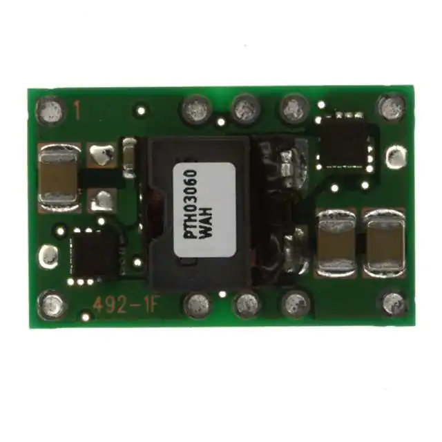


 工商网监
湘ICP备2023018690号
工商网监
湘ICP备2023018690号

