REG104
REG
104
REG
104
SBVS025G – SEPTEMBER 2001 – REVISED SEPTEMBER 2005
DMOS
1A Low-Dropout Regulator
FEATURES
DESCRIPTION
● NEW DMOS TOPOLOGY:
Ultra Low Dropout Voltage:
230mV typ at 1A and 3.3V Output
Output Capacitor NOT Required for Stability
● FAST TRANSIENT RESPONSE
● VERY LOW NOISE: 33µVRMS
● HIGH ACCURACY: ±2% max
● HIGH EFFICIENCY:
IGND = 1.7mA at IOUT = 1A
Not Enabled: IGND = 0.5µA
● 2.5V, 2.7V, 3.0V, 3.3V, 5.0V AND
ADJUSTABLE OUTPUT VERSIONS
● THERMAL PROTECTION
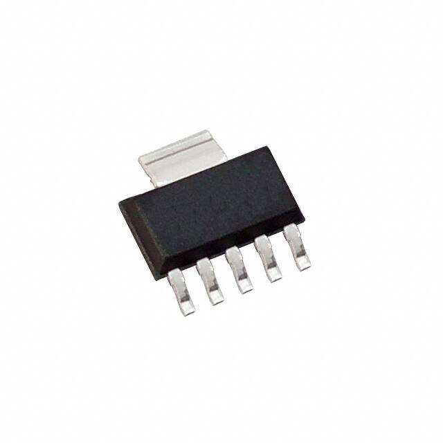
● SMALL SURFACE-MOUNT PACKAGES:
SOT223-5, DDPAK-5
The REG104 is a family of low-noise, low-dropout linear
regulators with low ground pin current. Its new DMOS topology provides significant improvement over previous designs,
including low dropout voltage (only 230mV typ at full load),
and better transient performance. In addition, no output
capacitor is required for stability, unlike conventional low
dropout regulators that are difficult to compensate and
require expensive low ESR capacitors greater than 1µF.
Typical ground pin current is only 1.7mA (at IOUT = 1A) and
drops to 0.5µA in not enabled mode. Unlike regulators with
PNP pass devices, quiescent current remains relatively constant over load variations and under dropout conditions.
The REG104 has very low output noise (typically 33µVRMS
for VOUT = 3.3V with CNR = 0.01µF), making it ideal for use
in portable communications equipment. On-chip trimming
results in high output voltage accuracy. Accuracy is maintained over temperature, line, and load variations. Key parameters are tested over the specified temperature range
(–40°C to +85°C).
APPLICATIONS
●
●
●
●
●
The REG104 is well protected—internal circuitry provides a
current limit which protects the load from damage. Thermal
protection circuitry keeps the chip from being damaged by
excessive temperature. The REG104 is available in the
DDPAK-5 and the SOT223-5.
PORTABLE COMMUNICATION DEVICES
BATTERY-POWERED EQUIPMENT
MODEMS
BAR-CODE SCANNERS
BACKUP POWER SUPPLIES
Enable
Enable
VOUT
VIN
+
0.1µF
NR
REG104
(Fixed Voltage
Versions)
+
COUT(1)
VIN
VOUT
+
0.1µF
REG104-A
R1
+
COUT(1)
Adj
Gnd
Gnd
R2
NR = Noise Reduction
NOTE: (1) Optional.
Please be aware that an important notice concerning availability, standard warranty, and use in critical applications of
Texas Instruments semiconductor products and disclaimers thereto appears at the end of this data sheet.
All trademarks are the property of their respective owners.
Copyright © 2001-2005, Texas Instruments Incorporated
PRODUCTION DATA information is current as of publication date.
Products conform to specifications per the terms of Texas Instruments
standard warranty. Production processing does not necessarily include
testing of all parameters.
www.ti.com
�ABSOLUTE MAXIMUM RATINGS(1)
Supply Input Voltage, VIN ....................................................... –0.3V to 16V
Enable Input Voltage, VEN ....................................................... –0.3V to VIN
Feedback Voltage, VFB ........................................................ –0.3V to 6.0V
NR Pin Voltage, VNR ............................................................. –0.3V to 6.0V
Output Short-Circuit Duration ...................................................... Indefinite
Operating Temperature Range ....................................... –55°C to +125°C
Storage Temperature Range .......................................... –65°C to +150°C
Junction Temperature ..................................................... –55°C to +150°C
Lead Temperature (soldering, 3s, SOT, and DDPAK) ................... +240°C
ESD Rating: HBM (VOUT to GND) ..................................................... 1.5kV
HBM (All other pins) ........................................................ 2kV
CDM .............................................................................. 500V
NOTE: (1) Stresses above these ratings may cause permanent damage.
Exposure to absolute maximum conditions for extended periods may degrade
device reliability.
ELECTROSTATIC
DISCHARGE SENSITIVITY
This integrated circuit can be damaged by ESD. Texas Instruments recommends that all integrated circuits be handled with
appropriate precautions. Failure to observe proper handling
and installation procedures can cause damage.
ESD damage can range from subtle performance degradation
to complete device failure. Precision integrated circuits may be
more susceptible to damage because very small parametric
changes could cause the device not to meet its published
specifications.
PACKAGE/ORDERING INFORMATION(1)
PRODUCT
VOUT
REG104xx-yyyy/zzz
XX is package designator.
YYYY is typical output voltage (5 = 5.0V, 2.85 = 2.85V, A = Adjustable).
ZZZ is package quantity.
(1) For the most current package and ordering information, see the Package Option Addendum at the end of this document, or see the TI website at www.ti.com.
PIN CONFIGURATIONS
Top View
SOT223-5
DDPAK-5
Tab is Gnd
Tab is Gnd
1 2 3 4 5
1
VO
Gnd
NR/Adjust(1)
VIN
Enable
(KTT Package)
2
VIN
VOUT
3
4
5
Gnd
Enable
NR/Adjust(1)
(DCQ Package)
NOTE: (1) For REG104A-A: voltage setting resistor pin.
All other models: noise reduction capacitor pin.
2
REG104
SBVS025G
�ELECTRICAL CHARACTERISTICS
Boldface limits apply over the specified temperature range, TJ = –40°C to +85°C
At TJ = +25°C, VIN = VOUT + 1V (VOUT = 3.0V for REG104-A), VENABLE = 2V, IOUT = 10mA, CNR = 0.01µF, and COUT = 0.1µF(1), unless otherwise noted.
REG104GA
REG104FA
PARAMETER
OUTPUT VOLTAGE
Output Voltage Range
REG104-2.5
REG104-2.7
REG104-3.0
REG104-3.3
REG104-5
REG104-A
Reference Voltage
Adjust Pin Current
Accuracy
TJ = –40°C to +85°C
vs Temperature
vs Line and Load
TJ = –40°C to +85°C
DC DROPOUT VOLTAGE(2, 3)
For all models except 5V
For 5V model
For all models except 5V
TJ = –40°C to +85°C
For 5V models
TJ = –40°C to +85°C
VOLTAGE NOISE
f = 10Hz to 100kHz
Without CNR (all models)
With CNR (all fixed voltage models)
OUTPUT CURRENT
Current Limit(4)
TJ = –40°C to +85°C
CONDITION
MIN
2.5
2.7
3.0
3.3
5
dVOUT/dT
VDROP
1.295
0.2
±0.5
TJ = –40°C to +85°C
IOUT = 10mA to 1A, VIN = (VOUT + 0.7V) to 15V
VIN = (VOUT + 0.9V) to 15V
IOUT
IOUT
IOUT
IOUT
=
=
=
=
70
±0.5
10mA
1A
1A
1A
3
230
320
IOUT = 1A
TEMPERATURE RANGE
Specified Range
Operating Range
Storage Range
Thermal Resistance
DDPAK-5 Surface Mount
SOT223-5 Surface Mount
±3.5
25
400
500
480
mV
mV
mV
mV
580
mV
1
±2
±3.0
±2.5
Vn
CNR = 0, COUT = 0
CNR = 0.01µF, COUT = 10µF
ICL
µVRMS
µVRMS
35µVRMS/V • VOUT
10µVRMS/V • VOUT
1.2
1.0
1.7
2.1
2.2
65
VENABLE
IENABLE
2
–0.2
VENABLE = 2V to VIN, VIN = 2.1V to 6.5(5)
VENABLE = 0V to 0.5V
1
2
50
1.5
IGND
IOUT = 10mA
IOUT = 1A
VENABLE ≤ 0.5V
0.5
1.7
0.5
A
A
dB
VIN
0.5
100
100
V
V
nA
nA
µs
ms
°C
°C
150
130
Enable Pin Low
INPUT VOLTAGE
Operating Input Voltage Range(6)
Specified Input Voltage Range
TJ = –40°C to +85°C
UNITS
V
V
V
V
V
V
V
µA
%
%
ppm/°C
%
%
5.5
VREF
VREF
IADJ
THERMAL SHUTDOWN
Junction Temperature
Shutdown
Reset from Shutdown
GROUND PIN CURRENT
Ground Pin Current
MAX
VOUT
RIPPLE REJECTION
f = 120Hz
ENABLE CONTROL
VENABLE High (output enabled)
VENABLE Low (output disabled)
IENABLE High (output enabled)
IENABLE Low (output disabled)
Output Disable Time
Output Enable Softstart Time
TYP
0.7
1.8
mA
mA
µA
2.1
VOUT + 0.7
VOUT + 0.9
15
15
15
V
V
V
–40
–55
–65
+85
+125
+150
°C
°C
°C
VIN
VIN > 2.7V
VIN > 2.9V
TJ
θJC
θJC
Junction-to-Case
Junction-to-Case
4
15
°C/W
°C/W
NOTES: (1) The REG104 does not require a minimum output capacitor for stability. However, transient response can be improved with proper capacitor selection.
(2) Dropout voltage is defined as the input voltage minus the output voltage that produces a 2% change in the output voltage from the value at VIN = VOUT + 1V
at fixed load.
(3) Not applicable for VOUT less than 2.7V.
(4) Current limit is the output current that produces a 15% change in output voltage from VIN = VOUT + 1V and IOUT = 10mA.
(5) For VIN > 6.5V, see typical characteristic VENABLE vs IENABLE.
(6) The REG104 no longer regulates when VIN < VOUT + VDROP (MAX). In drop-out or when the input voltage is between 2.7V and 2.1V, the impedance from VIN
to VOUT is typically less than 1Ω at TJ = +25°C. See typical characteristic Output Voltage Change vs VIN.
REG104
SBVS025G
3
�TYPICAL CHARACTERISTICS
For all models, at TJ = +25°C and VENABLE = 2V, unless otherwise noted.
OUTPUT VOLTAGE CHANGE vs IOUT
(VIN = VOUT + 1V, Output Voltage % Change
Referred to IOUT = 10mA at +25°C)
DC DROPOUT VOLTAGE vs IOUT
350
0.8
300
+125°C
0.4
DC Dropout Voltage (mV)
Output Voltage Change (%)
0.6
0.2
0
+25°C
–0.2
–0.4
–0.6
–0.8
–55°C
+125°C
250
+25°C
200
–55°C
150
100
50
–1
0
–1.2
0
100
200 300 400
500 600
700
0
800 900 1000
400
600
800
IOUT (mA)
OUTPUT VOLTAGE CHANGE vs VIN
OUTPUT VOLTAGE CHANGE vs IOUT
(Output Voltage % Change Referred to
VIN = VOUT + 1V at IOUT = 10mA)
(Output Voltage % Change Referred to
IOUT = 10mA at +25°C)
1000
0.6
0.5
IOUT = 10mA
IOUT = 200mA
0.4
0
IOUT = 10mA
0.2
Output Voltage (%)
Output Voltage Change (%)
200
Output Current (mA)
IOUT = 1000mA
–0.5
–1
IOUT = 200mA
0
–0.2
IOUT = 1000mA
–0.4
–0.6
–0.8
–1.5
–1
–2
0
2
4
6
8
10
–1.2
–60
12
20
40
60
80
100
DC DROPOUT VOLTAGE vs TEMPERATURE
LINE REGULATION vs TEMPERATURE
(VIN = VOUT + 1V to 16V)
120
0.5
Output Voltage Change (%)
DC Dropout Voltage (mV)
0
Input Voltage Above VOUT (V)
300
IOUT = 1000mA
250
200
150
100
IOUT = 200mA
50
0.4
0.3
IOUT = 10mA
0.2
0.1
IOUT = 200mA
IOUT = 10mA
–50
–25
0
25
50
Temperature (°C)
4
–20
Temperature (°C)
350
0
–75
–40
75
100
125
0
–75
–50
–25
0
25
50
75
100
125
Temperature (°C)
REG104
SBVS025G
�TYPICAL CHARACTERISTICS (Cont.)
For all models, at TJ = +25°C and VENABLE = 2V, unless otherwise noted.
LOAD TRANSIENT RESPONSE
LINE TRANSIENT RESPONSE
50mV/div
500mV/div
REG104-3.3
COUT = 0
500mV/div
VOUT
1A
VOUT
50mV/div
COUT = 10µF
ILOAD
6V
VOUT
COUT = 10µF
VOUT
VIN
5V
10µs/div
50µs/div
LOAD TRANSIENT RESPONSE
LOAD TRANSIENT RESPONSE
REG104–A
REG104–A
CFB = 0.01µF, VOUT = 3.3V
Load = 200mA, CFB = 0.01µF, VOUT = 3.3V
50mV/div 50mV/div
500mV/div 500mV/div
10mA
REG104-3.3
IOUT = 200mA
COUT = 0
COUT = 0
COUT = 10µF
1A
COUT = 0
COUT = 10µF
6V
ILOAD
VIN
5V
10mA
10µs/div
50µs/div
LOAD REGULATION vs TEMPERATURE
(VIN = VOUT + 1V and 10mA < IOUT < 1000mA)
OUTPUT NOISE DENSITY
10
0.5
Noise Density (µV/√Hz)
Output Voltage Change (%)
5
0.4
0.3
0.2
0.1
2
1
0.5
0.2
CNR = 0
COUT = 0
0.1
0.05
CNR = 0.01µF
COUT = 10µF
0.02
0
–60
0.01
–40
–20
0
20
40
60
Temperature (°C)
REG104
SBVS025G
80
100
120
10
100
1000
10000
100,000
Frequency (Hz)
5
�TYPICAL CHARACTERISTICS (Cont.)
For all models, at TJ = +25°C and VENABLE = 2V, unless otherwise noted.
GROUND PIN CURRENT, NOT ENABLED
vs TEMPERATURE
GROUND PIN CURRENT vs TEMPERATURE
3
1.8
VENABLE = 0V
IOUT = 1000mA
1.6
2.5
2
IGND (µA)
IGND (mA)
1.4
1.2
1
IOUT = 200mA
0.8
1.5
1
0.5
0.6
IOUT = 10mA
0.4
–60
–40
–20
0
20
40
60
80
100
0
–75
120
–50
–25
0
25
50
75
100
125
Temperature (°C)
Temperature (°C)
IADJUST vs TEMPERATURE
GROUND PIN CURRENT vs IOUT
1.6
0.28
1.4
0.26
Adjust Pin Current (µA)
REG104-A
IGND (mA)
1.2
1
0.8
0.6
0.24
0.22
0.20
0.18
0.16
0.4
1
10
100
1000
0.14
–60 –40 –20
0
20
40
60
80
100 120
140
Temperature (°C)
IOUT (mA)
RIPPLE REJECTION vs FREQUENCY
CURRENT LIMIT vs TEMPERATURE
70
1850
VOUT = VOUT-NOMINAL • 0.90
60
Ripple Rejection (dB)
Current Limit (mA)
1800
1750
VOUT = 1V
1700
1650
COUT = 0
20
–40
–20
0
20
40
60
Temperature (°C)
6
COUT = 10µF
40
30
1600
1550
–60
50
80
100
120
10
100
1k
10k
100k
Frequency (Hz)
REG104
SBVS025G
�TYPICAL CHARACTERISTICS (Cont.)
For all models, at TJ = +25°C and VENABLE = 2V, unless otherwise noted.
RIPPLE REJECTION vs IOUT
SOFT START
75
VRIPPLE = 3Vp-p, f = 120Hz
1V/div
Ripple Rejection (dB)
70
65
VOUT
60
55
50
45
2V
VENABLE
0
40
0
200
400
600
800
1000
250µs/div
IOUT (mA)
OUTPUT DISABLE TIME
OUTPUT VOLTAGE DRIFT HISTOGRAM
45
1V/div
COUT = 0
40
35
Percent of Units (%)
VOUT
2V
VENABLE
30
25
20
15
10
5
0
0
10µs/div
40
45
50
55
60
65
70
75
80
85
90
VOUT Drift (ppm/°C)
OUTPUT VOLTAGE ACCURACY HISTOGRAM
60
Percent of Units (%)
50
40
30
20
10
0
–1 –0.8 –0.6 –0.4 –0.2
0
0.2 0.4
0.6 0.8
1
Error (%)
REG104
SBVS025G
7
�BASIC OPERATION
The REG104 series is a family of LDO (Low DropOut) linear
regulators. The family includes five fixed output versions
(2.5V to 5.0V) and an adjustable output version. An internal
DMOS power device provides low dropout regulation with
near constant ground pin current (largely independent of load
and dropout conditions) and very fast line and load transient
response. All versions include internal current limit and
thermal shutdown circuitry.
Figure 1 shows the basic circuit connections for the fixed
voltage models. Figure 2 gives the connections for the
adjustable output version (REG104A) and example resistor
values for some commonly used output voltages. Values for
other voltages can be calculated from the equation shown in
Figure 2.
None of the versions require an output capacitor for regulator
stability. The REG104 will accept any output capacitor type
less than 1µF. For capacitance values larger than 1µF the
effective ESR should be greater than 0.1Ω. This minimum
ESR value includes parasitics such as printed circuit board
traces, solder joints, and sockets. A minimum 0.1µF low ESR
capacitor connected to the input supply voltage is recommended.
ENABLE
The Enable pin allows the regulator to be turned on and off.
This pin is active HIGH and compatible with standard TTLCMOS levels. Inputs below 0.5V (max) turn the regulator off
and all circuitry is disabled. Under this condition ground-pin
current drops to approximately 0.5µA.
When not used, the Enable pin may be connected to VIN.
Internal to the part, the Enable pin is connected to an input
resistor-zener diode circuit, as shown in Figure 3, creating a
nonlinear input impedance.
Enable
VIN
In
REG104
Gnd
0.1µF
VOUT
Out
NR
Enable
COUT
175kΩ
CNR
0.01µF
VZ = 10V
Optional
FIGURE 3. Enable Pin Equivalent Input Circuit.
FIGURE 1. Fixed Voltage Nominal Circuit for REG104.
Enable
5
2
VOUT
1
VIN
REG104
4
0.1µF
IADJ
3 Gnd
R1
CFB
0.01µF
EXAMPLE RESISTOR VALUES
R1 (Ω)(1)
R2 (Ω)(1)
1.295
Short
Open
2.5
12.1k
1.21k
13k
1.3k
3
16.9k
1.69k
13k
1.3k
3.3
20k
2.0k
13k
1.3k
5
37.4k
3.74k
13k
1.3k
VOUT (V)
COUT
Load
Adj
R2
Pin numbers for SOT-223 package.
Optional
VOUT = (1 + R1/R2) • 1.295V
To reduce current through divider, increase resistor
values (see table at right).
NOTE: (1) Resistors are standard 1% values.
As the impedance of the resistor divider increases,
IADJ (~200nA) may introduce an error.
CFB improves noise and transient response.
FIGURE 2. Adjustable Voltage Circuit for REG104A.
8
REG104
SBVS025G
�The Enable Pin Current versus Applied Voltage relationship
is shown in Figure 4. When the Enable pin is connected to
VIN greater than 10V, a series resistor may be used to limit
the current.
VN = 35
µVRMS
• VOUT
V
Connecting a capacitor, CNR, from the Noise-Reduction (NR)
pin to ground can reduce the output noise voltage. Adding
CNR, as shown in Figure 5, forms a low-pass filter for the
voltage reference. For CNR = 10nF, the total noise in the
10Hz to 100kHz bandwidth is reduced by approximately
a factor of 3.5. This noise reduction effect is shown in
Figure 6.
100
10
Enable Current (µA)
Since the value of VREF is 1.295V, this relationship reduces to:
1
0.1
45
REG104-3.3
0.001
0
2
4
6
8
10
12
14
16
Enable Voltage
FIGURE 4. Enable Pin Current versus Applied Voltage.
Output Noise Voltage
(µVRMS 10Hz - 100kHz)
0.01
35
OUTPUT NOISE
A precision band-gap reference is used for the internal
reference voltage, VREF, for the REG104. This reference is
the dominant noise source within the REG104. It generates
approximately 45µVRMS in the 10Hz to 100kHz bandwidth at
the reference output. The regulator control loop gains up the
reference noise, so that the noise voltage of the regulator is
approximately given by:
VN = 45µVRMS
V
R1 + R 2
= 45µVRMS • OUT
R2
VREF
COUT = 0
COUT = 10µF
25
0.001
0.01
0.1
1
CNR (µF)
FIGURE 6. Output Noise versus Noise Reduction Capacitor.
The REG104 adjustable version does not have the noisereduction pin available, however, the adjust pin is the
summing junction of the error amplifier. A capacitor, CFB,
VIN
NR
(fixed output
versions only)
Low Noise
Charge Pump
CNR
(optional)
Enable
VREF
(1.295V)
DMOS
Output
VOUT
Over Current
Over Temp
Protection
R1
R2
Adj
(Adjustable
Versions)
REG104
NOTE: R1 and R2 are internal
on fixed output versions.
FIGURE 5. Block Diagram.
REG104
SBVS025G
9
�connected from the output to the adjust pin will reduce both
the output noise and the peak error from a load transient.
Figure 7 shows improved output noise performance for two
capacitor combinations.
nV/√Hz
10.0
In the transient dropout region between DC and Transient,
transient response recovery time increases. The time required to recover from a load transient is a function of both
the magnitude and rate of the step change in load current
and the available headroom VIN to VOUT voltage drop. Under
worst-case conditions (full-scale load change with VIN to
VOUT voltage drop close to DC dropout levels), the REG104
can take several hundred microseconds to re-enter the
specified window of regulation.
1.0
COUT = 0, CFB = 0
COUT = 0, CFB = 0.01µF
COUT = 10µF, CFB = 0.01µF
0.1
10
100
1000
10000
100000
Frequency
FIGURE 7. Output Noise Density on Adjustable Versions.
The REG104 utilizes an internal charge pump to develop an
internal supply voltage sufficient to drive the gate of the
DMOS pass element above VIN. The charge-pump switching
noise (nominal switching frequency = 2MHz) is not measurable at the output of the regulator.
DROP-OUT VOLTAGE
The REG104 uses an N-channel DMOS as the pass element. When the input voltage is within a few hundred
millivolts of the output voltage, the DMOS device behaves
like a resistor. Therefore, for low values of VIN to VOUT, the
regulator’s input-to-output resistance is the RdsON of the
DMOS pass element (typically 230mΩ). For static (DC)
loads, the REG104 will typically maintain regulation down to
VIN to VOUT voltage drop of 230mV at full rated output current.
In Figure 8, the bottom line (DC dropout) shows the minimum
VIN to VOUT voltage drop required to prevent dropout under
DC load conditions.
REG104 –3.3 at 25°C
250
DC
Transient
Drop Out Voltage (mV)
For large step changes in load current, the REG104 requires
a larger voltage drop across it to avoid degraded transient
response. The boundary of this transient dropout region is
shown as the top line in Figure 8. Values of VIN to VOUT
voltage drop above this line insure normal transient response.
200
150
TRANSIENT RESPONSE
The REG104 response to transient line and load conditions
improves at lower output voltages. The addition of a capacitor (nominal value 10nF) from the output pin to ground may
improve the transient response. In the adjustable version, the
addition of a capacitor, CFB (nominal value 10nF), from the
output to the adjust pin will also improve the transient
response.
THERMAL PROTECTION
Power dissipated within the REG104 will cause the junction
temperature to rise. The REG104 has thermal shutdown
circuitry that protects the regulator from damage. The thermal protection circuitry disables the output when the junction temperature reaches approximately 150°C, allowing
the device to cool. When the junction temperature cools to
approximately 130°C, the output circuitry is again enabled.
Depending on various conditions, the thermal protection
circuit may cycle on and off. This limits the dissipation of the
regulator, but may have an undesirable effect on the load.
Any tendency to activate the thermal protection circuit indicates excessive power dissipation or an inadequate heat
sink. For reliable operation, junction temperature should be
limited to 125°C, maximum. To estimate the margin of safety
in a complete design (including heat sink), increase the
ambient temperature until the thermal protection is triggered.
Use worst-case loads and signal conditions. For good reliability, thermal protection should trigger more than 35°C
above the maximum expected ambient condition of your
application. This produces a worst-case junction temperature
of 125°C at the highest expected ambient temperature and
worst-case load.
The internal protection circuitry of the REG104 has been
designed to protect against overload conditions. It was not
intended to replace proper heat sinking. Continuously running the REG104 into thermal shutdown will degrade reliability.
100
50
0
0
100
200
300
400
500
IOUT (mA)
FIGURE 8. Transient and DC Dropout.
10
REG104
SBVS025G
�POWER DISSIPATION
Power dissipation depends on input voltage and load conditions. Power dissipation is equal to the product of the average output current times the voltage across the output
element, VIN to VOUT voltage drop.
PD = (VIN – VOUT ) • IOUT ( AVG)
Power dissipation can be minimized by using the lowest
possible input voltage necessary to assure the required
output voltage.
REG104
SBVS025G
5
Power Dissipation (Watts)
The REG104 is available in two different package configurations. The ability to remove heat from the die is different for
each package type and, therefore, presents different considerations in the printed circuit board (PCB) layout. The PCB
area around the device that is free of other components
moves the heat from the device to the ambient air. While it
is difficult to impossible to quantify all of the variables in a
thermal design of this type, performance data for several
configurations are shown in Figure 9. In all cases the PCB
copper area is bare copper, free of solder resist mask, and
not solder plated. All examples are for 1-ounce copper. Using
heavier copper will increase the effectiveness in moving the
heat from the device. In those examples where there is
copper on both sides of the PCB, no connection has been
provided between the two sides. The addition of plated
through holes will improve the heat sink effectiveness.
CONDITIONS
#1
#2
#3
#4
4
3
2
1
0
0
25
50
75
100
125
Ambient Temperature (°C)
CONDITION
PACKAGE
PCB AREA
θJA
27°C/W
1
DDPAK
4in2 Top Side Only
2
SOT-223
4in2 Top Side Only
53°C/W
3
DDPAK
None
65°C/W
4
SOT-223
0.5in2 Top Side Only
110°C/W
FIGURE 9. Maximum Power Dissipation versus Ambient
Temperature for the Various Packages and
PCB Heat Sink Configurations.
11
�REGULATOR MOUNTING
The tab of both packages is electrically connected to ground.
For best thermal performance, the tab of the DDPAK surface-mount version should be soldered directly to a circuitboard copper area. Increasing the copper area improves
heat dissipation. Figure 10 shows typical thermal resistance
from junction to ambient as a function of the copper area for
the DDPAK. Figure 11 shows the same relationship for the
SOT-223.
Although the tabs of the DDPAK and the SOT-223 are
electrically grounded, they are not intended to carry any
current. The copper pad that acts as a heat sink should be
isolated from the rest of the circuit to prevent current flow
through the device from the tab to the ground pin. Solder pad
footprint recommendations for the various REG104 devices
are presented in the Application Bulletin Solder Pad Recommendations for Surface-Mount Devices (SBFA015A), available from the Texas Instruments web site (www.ti.com).
THERMAL RESISTANCE vs PCB COPPER AREA
Thermal Resistance, θJA (°C/W)
50
Circuit Board Copper Area
REG104
Surface Mount Package
1 oz. copper
40
30
20
10
REG104
DDPAK Surface Mount Package
0
0
1
2
3
4
5
Copper Area (inches2)
FIGURE 10. Thermal Resistance versus PCB Area for the Five-Lead DDPAK.
THERMAL RESISTANCE vs PCB COPPER AREA
Thermal Resistance, θJA (°C/W)
180
Circuit Board Copper Area
REG104
Surface Mount Package
1 oz. copper
160
140
120
100
80
60
40
20
REG104
SOT-223 Surface Mount Package
0
0
1
2
3
4
5
Copper Area (inches2)
FIGURE 11. Thermal Resistance versus PCB Area for the Five Lead SOT-223.
12
REG104
SBVS025G
�PACKAGE OPTION ADDENDUM
www.ti.com
14-Oct-2022
PACKAGING INFORMATION
Orderable Device
Status
(1)
Package Type Package Pins Package
Drawing
Qty
Eco Plan
(2)
Lead finish/
Ball material
MSL Peak Temp
Op Temp (°C)
Device Marking
(3)
Samples
(4/5)
(6)
(1)
REG104FA-2.5KTTT
ACTIVE
DDPAK/
TO-263
KTT
5
50
RoHS & Green
Call TI | SN
Level-2-260C-1 YEAR
REG
104FA-2.5
Samples
REG104FA-2.5KTTTG3
ACTIVE
DDPAK/
TO-263
KTT
5
50
RoHS & Green
SN
Level-2-260C-1 YEAR
REG
104FA-2.5
Samples
REG104FA-3.3/500
ACTIVE
DDPAK/
TO-263
KTT
5
500
RoHS & Green
Call TI | SN
Level-2-260C-1 YEAR
REG
104FA-3.3
Samples
REG104FA-5/500
ACTIVE
DDPAK/
TO-263
KTT
5
500
RoHS & Green
Call TI | SN
Level-2-260C-1 YEAR
REG
104FA-5
Samples
REG104FA-5/500G3
ACTIVE
DDPAK/
TO-263
KTT
5
500
RoHS & Green
SN
Level-2-260C-1 YEAR
REG
104FA-5
Samples
REG104FA-A/500
ACTIVE
DDPAK/
TO-263
KTT
5
500
RoHS & Green
Call TI | SN
Level-2-260C-1 YEAR
REG
104FA-A
Samples
REG104GA-2.5
ACTIVE
SOT-223
DCQ
6
78
RoHS & Green
NIPDAU
Level-2-260C-1 YEAR
R104G25
Samples
REG104GA-2.5/2K5
ACTIVE
SOT-223
DCQ
6
2500
RoHS & Green
NIPDAU
Level-2-260C-1 YEAR
R104G25
Samples
REG104GA-3.3
ACTIVE
SOT-223
DCQ
6
78
RoHS & Green
NIPDAU
Level-2-260C-1 YEAR
R104G33
Samples
REG104GA-3.3/2K5
ACTIVE
SOT-223
DCQ
6
2500
RoHS & Green
NIPDAU
Level-2-260C-1 YEAR
R104G33
Samples
REG104GA-3.3G4
ACTIVE
SOT-223
DCQ
6
78
RoHS & Green
NIPDAU
Level-2-260C-1 YEAR
R104G33
Samples
REG104GA-5
ACTIVE
SOT-223
DCQ
6
78
RoHS & Green
SN
Level-2-260C-1 YEAR
R104G50
Samples
REG104GA-5/2K5
ACTIVE
SOT-223
DCQ
6
2500
RoHS & Green
SN
Level-2-260C-1 YEAR
-40 to 85
R104G50
Samples
REG104GA-5/2K5G4
ACTIVE
SOT-223
DCQ
6
2500
RoHS & Green
NIPDAU
Level-2-260C-1 YEAR
-40 to 85
R104G50
Samples
REG104GA-5G4
ACTIVE
SOT-223
DCQ
6
78
RoHS & Green
NIPDAU
Level-2-260C-1 YEAR
R104G50
Samples
REG104GA-A
ACTIVE
SOT-223
DCQ
6
78
RoHS & Green
SN
Level-2-260C-1 YEAR
-40 to 85
R104GA
Samples
REG104GA-A/2K5
ACTIVE
SOT-223
DCQ
6
2500
RoHS & Green
NIPDAU | SN
Level-2-260C-1 YEAR
-40 to 85
R104GA
Samples
REG104GA-AG4
ACTIVE
SOT-223
DCQ
6
78
RoHS & Green
NIPDAU
Level-2-260C-1 YEAR
-40 to 85
R104GA
Samples
The marketing status values are defined as follows:
Addendum-Page 1
-40 to 85
-40 to 85
�PACKAGE OPTION ADDENDUM
www.ti.com
14-Oct-2022
ACTIVE: Product device recommended for new designs.
LIFEBUY: TI has announced that the device will be discontinued, and a lifetime-buy period is in effect.
NRND: Not recommended for new designs. Device is in production to support existing customers, but TI does not recommend using this part in a new design.
PREVIEW: Device has been announced but is not in production. Samples may or may not be available.
OBSOLETE: TI has discontinued the production of the device.
(2)
RoHS: TI defines "RoHS" to mean semiconductor products that are compliant with the current EU RoHS requirements for all 10 RoHS substances, including the requirement that RoHS substance
do not exceed 0.1% by weight in homogeneous materials. Where designed to be soldered at high temperatures, "RoHS" products are suitable for use in specified lead-free processes. TI may
reference these types of products as "Pb-Free".
RoHS Exempt: TI defines "RoHS Exempt" to mean products that contain lead but are compliant with EU RoHS pursuant to a specific EU RoHS exemption.
Green: TI defines "Green" to mean the content of Chlorine (Cl) and Bromine (Br) based flame retardants meet JS709B low halogen requirements of


 工商网监
湘ICP备2023018690号
工商网监
湘ICP备2023018690号
