SN74AHC4066
QUADRUPLE BILATERAL ANALOG SWITCH
SCLS511 − JUNE 2003
D 2-V to 5.5-V VCC Operation
D Supports Mixed-Mode Voltage Operation on
All Ports
High On-Off Output-Voltage Ratio
Low Crosstalk Between Switches
Individual Switch Controls
Extremely Low Input Current
ESD Protection Exceeds JESD 22
− 2000-V Human-Body Model (A114-A)
− 200-V Machine Model (A115-A)
− 1000-V Charged-Device Model (C101)
1A
1B
2B
2A
2C
3C
GND
1
14
2
13
3
12
4
11
5
10
6
9
7
8
VCC
1C
4C
4A
4B
3B
3A
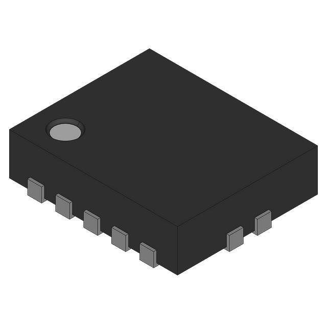
RGY PACKAGE
(TOP VIEW)
1B
2B
2A
2C
3C
This switch is designed to handle both analog and
digital signals. Each switch permits signals with
amplitudes up to 5.5 V (peak) to be transmitted in
either direction.
VCC
This quadruple silicon-gate CMOS analog switch
is designed for 2-V to 5.5-V VCC operation.
1A
description/ordering information
1
14
2
13 1C
3
12 4C
4
11 4A
5
10 4B
9 3B
6
Each switch section has its own enable-input
control (C). A high-level voltage applied to C turns
on the associated switch section.
GND
7
Applications include signal gating, chopping,
modulation or demodulation (modem), and signal
multiplexing
for
analog-to-digital
and
digital-to-analog conversion systems.
8
3A
D
D
D
D
D
D, DB, DGV, N, NS, OR PW PACKAGE
(TOP VIEW)
NC − No internal connection
ORDERING INFORMATION
Tube
SN74AHC4066N
SN74AHC4066N
QFN − RGY
Tape and reel
SN74AHC4066RGYR
HA4066
Tube
SN74AHC4066D
Tape and reel
SN74AHC4066DR
Tube
SN74AHC4066NS
Tape and reel
SN74AHC4066NSR
Tube
SN74AHC4066DB
Tape and reel
SN74AHC4066DBR
Tube
SN74AHC4066PW
Tape and reel
SN74AHC4066PWR
Tape and reel
SN74AHC4066DGVR
SOP − NS
SSOP − DB
TSSOP − PW
TVSOP − DGV
†
TOP-SIDE
MARKING
PDIP − N
SOIC − D
−40°C to 85°C
ORDERABLE
PART NUMBER
PACKAGE†
TA
AHC4066
AHC4066
HA4066
HA4066
HA4066
Package drawings, standard packing quantities, thermal data, symbolization, and PCB design guidelines
are available at www.ti.com/sc/package.
Please be aware that an important notice concerning availability, standard warranty, and use in critical applications of
Texas Instruments semiconductor products and disclaimers thereto appears at the end of this data sheet.
Copyright © 2003, Texas Instruments Incorporated
PRODUCTION DATA information is current as of publication date.
Products conform to specifications per the terms of Texas Instruments
standard warranty. Production processing does not necessarily include
testing of all parameters.
POST OFFICE BOX 655303
• DALLAS, TEXAS 75265
1
�SN74AHC4066
QUADRUPLE BILATERAL ANALOG SWITCH
SCLS511 − JUNE 2003
FUNCTION TABLE
(each switch)
INPUT
CONTROL
(C)
SWITCH
L
OFF
H
ON
logic diagram (positive logic)
A
VCC
VCC
B
C
One of Four Switches
absolute maximum ratings over operating free-air temperature range (unless otherwise noted)†
Supply voltage range, VCC (see Note 1) . . . . . . . . . . . . . . . . . . . . . . . . . . . . . . . . . . . . . . . . . . . . . . −0.5 V to 7 V
Input voltage range, VI (see Note 1) . . . . . . . . . . . . . . . . . . . . . . . . . . . . . . . . . . . . . . . . . . . . . . . . . . −0.5 V to 7 V
Switch I/O voltage range, VIO (see Notes 1 and 2) . . . . . . . . . . . . . . . . . . . . . . . . . . . . . . . −0.5 V to VCC + 0.5 V
Control-input clamp current, IIK (VI < 0) . . . . . . . . . . . . . . . . . . . . . . . . . . . . . . . . . . . . . . . . . . . . . . . . . . . . −20 mA
I/O diode current, IIOK (VIO < 0 or VIO > VCC) . . . . . . . . . . . . . . . . . . . . . . . . . . . . . . . . . . . . . . . . . . . . . . . ±50 mA
On-state switch current, IT (VIO = 0 to VCC) . . . . . . . . . . . . . . . . . . . . . . . . . . . . . . . . . . . . . . . . . . . . . . . . . ±25 mA
Continuous current through VCC or GND . . . . . . . . . . . . . . . . . . . . . . . . . . . . . . . . . . . . . . . . . . . . . . . . . . . ±50 mA
Package thermal impedance, θJA (see Note 3): D package . . . . . . . . . . . . . . . . . . . . . . . . . . . . . . . . . . . 86°C/W
(see Note 3): DB package . . . . . . . . . . . . . . . . . . . . . . . . . . . . . . . . . 96°C/W
(see Note 3): DGV package . . . . . . . . . . . . . . . . . . . . . . . . . . . . . . . 127°C/W
(see Note 3): N package . . . . . . . . . . . . . . . . . . . . . . . . . . . . . . . . . . . 80°C/W
(see Note 3): NS package . . . . . . . . . . . . . . . . . . . . . . . . . . . . . . . . . 76°C/W
(see Note 3): PW package . . . . . . . . . . . . . . . . . . . . . . . . . . . . . . . . 113°C/W
(see Note 4): RGY package . . . . . . . . . . . . . . . . . . . . . . . . . . . . . . . . 47°C/W
Storage temperature range, Tstg . . . . . . . . . . . . . . . . . . . . . . . . . . . . . . . . . . . . . . . . . . . . . . . . . . . −65°C to 150°C
†
Stresses beyond those listed under “absolute maximum ratings” may cause permanent damage to the device. These are stress ratings only, and
functional operation of the device at these or any other conditions beyond those indicated under “recommended operating conditions” is not
implied. Exposure to absolute-maximum-rated conditions for extended periods may affect device reliability.
NOTES: 1. The input and output voltage ratings may be exceeded if the input and output current ratings are observed.
2. This value is limited to 5.5 V maximum.
3. The package thermal impedance is calculated in accordance with JESD 51-7.
4. The package thermal impedance is calculated in accordance with JESD 51-5.
2
POST OFFICE BOX 655303
• DALLAS, TEXAS 75265
�SN74AHC4066
QUADRUPLE BILATERAL ANALOG SWITCH
SCLS511 − JUNE 2003
recommended operating conditions (see Note 5)
VCC
Supply voltage
VCC = 2 V
VIH
High level input voltage,
High-level
voltage control inputs
MIN
MAX
2†
5.5
Low level input voltage,
Low-level
voltage control inputs
V
1.5
VCC = 2.3 V to 2.7 V
VCC × 0.7
VCC = 3 V to 3.6 V
VCC × 0.7
VCC = 4.5 V to 5.5 V
VCC × 0.7
VCC = 2 V
VIL
UNIT
V
0.5
VCC = 2.3 V to 2.7 V
VCC × 0.3
VCC = 3 V to 3.6 V
VCC × 0.3
VCC = 4.5 V to 5.5 V
VCC × 0.3
V
VI
Control input voltage
0
5.5
V
VIO
Input/output voltage
0
VCC
V
Δt/Δv
Input transition rise or fall rate
VCC = 2.3 V to 2.7 V
200
VCC = 3 V to 3.6 V
100
VCC = 4.5 V to 5.5 V
TA
Operating free-air temperature
ns/V
20
−40
85
°C
†
With supply voltages at or near 2 V, the analog switch on-state resistance becomes very nonlinear. Only digital signals should be transmitted
at these low supply voltages.
NOTE 5: All unused inputs of the device must be held at VCC or GND to ensure proper device operation. Refer to the TI application report,
Implications of Slow or Floating CMOS Inputs, literature number SCBA004.
POST OFFICE BOX 655303
• DALLAS, TEXAS 75265
3
�SN74AHC4066
QUADRUPLE BILATERAL ANALOG SWITCH
SCLS511 − JUNE 2003
electrical characteristics over recommended operating free-air temperature range (unless
otherwise noted)
PARAMETER
VCC
TA = 25°C
MIN
TYP
MAX
MIN
MAX
UNIT
IT = −1 mA,,
VI = VCC or GND,
VC = VIH
(see Figure 1)
2.3 V
38
180
225
3V
29
150
190
4.5 V
21
75
100
IT = −1 mA,
VI = VCC to GND,
VC = VIH
2.3 V
143
500
600
3V
57
180
225
4.5 V
31
100
125
Difference in
on-state
on
state resistance
between switches
IT = −1 mA,
VI = VCC to GND,
VC = VIH
2.3 V
6
30
40
3V
3
20
30
4.5 V
2
15
20
Control input current
VI = 5.5 V or GND
0 to 5.5 V
±0.1
±1
μA
IS(off)
Off-state
switch leakage
current
VI = VCC and
VO = GND, or
VI = GND and
VO = VCC,
VC = VIL
(see Figure 2)
5.5 V
±0.1
±1
μA
IS(on)
On-state
switch leakage
current
VI = VCC or GND,
VC = VIH
(see Figure 3)
5.5 V
±0.1
±1
μA
ICC
Supply current
VI = VCC or GND
5.5 V
20
μA
Cic
Control input
capacitance
1.5
pF
Cio
Switch input/output
capacitance
5.5
pF
CF
Feed-through
capacitance
0.5
pF
ron
ron(p)
Δron
II
4
TEST CONDITIONS
On-state
switch resistance
P k
Peak
on-state resistance
POST OFFICE BOX 655303
• DALLAS, TEXAS 75265
Ω
Ω
Ω
�SN74AHC4066
QUADRUPLE BILATERAL ANALOG SWITCH
SCLS511 − JUNE 2003
switching characteristics over recommended operating free-air temperature range,
VCC = 2.5 V ± 0.2 V (unless otherwise noted)
PARAMETER
FROM
(INPUT)
TO
(OUTPUT)
TEST
CONDITIONS
TA = 25°C
MIN
TYP
MAX
MIN
MAX
UNIT
tPLH
tPHL
Propagation
delay time
A or B
B or A
CL = 15 pF,
(see Figure 4)
1.2
10
16
ns
tPZH
tPZL
Switch
turn-on time
C
A or B
CL = 15 pF,
RL = 1 kΩ
(see Figure 5)
3.3
15
20
ns
tPLZ
tPHZ
Switch
turn-off time
C
A or B
CL = 15 pF,
RL = 1 kΩ
(see Figure 5)
6
15
23
ns
tPLH
tPHL
Propagation
delay time
A or B
B or A
CL = 50 pF,
(see Figure 4)
2.6
12
18
ns
tPZH
tPZL
Switch
turn-on time
C
A or B
CL = 50 pF,
RL = 1 kΩ
(see Figure 5)
4.2
25
32
ns
tPLZ
tPHZ
Switch
turn-off time
C
A or B
CL = 50 pF,
RL = 1 kΩ
(see Figure 5)
9.6
25
32
ns
switching characteristics over recommended operating free-air temperature range,
VCC = 3.3 V ± 0.3 V (unless otherwise noted)
PARAMETER
FROM
(INPUT)
TO
(OUTPUT)
TEST
CONDITIONS
TA = 25°C
MIN
TYP
MAX
MIN
MAX
UNIT
tPLH
tPHL
Propagation
delay time
A or B
B or A
CL = 15 pF,
(see Figure 4)
0.8
6
10
ns
tPZH
tPZL
Switch
turn-on time
C
A or B
CL = 15 pF,
RL = 1 kΩ
(see Figure 5)
2.3
11
15
ns
tPLZ
tPHZ
Switch
turn-off time
C
A or B
CL = 15 pF,
RL = 1 kΩ
(see Figure 5)
4.5
11
15
ns
tPLH
tPHL
Propagation
delay time
A or B
B or A
CL = 50 pF,
(see Figure 4)
1.5
9
12
ns
tPZH
tPZL
Switch
turn-on time
C
A or B
CL = 50 pF,
RL = 1 kΩ
(see Figure 5)
3
18
22
ns
tPLZ
tPHZ
Switch
turn-off time
C
A or B
CL = 50 pF,
RL = 1 kΩ
(see Figure 5)
7.2
18
22
ns
POST OFFICE BOX 655303
• DALLAS, TEXAS 75265
5
�SN74AHC4066
QUADRUPLE BILATERAL ANALOG SWITCH
SCLS511 − JUNE 2003
switching characteristics over recommended operating free-air temperature range,
VCC = 5 V ± 0.5 V (unless otherwise noted)
PARAMETER
FROM
(INPUT)
TO
(OUTPUT)
TEST
CONDITIONS
TA = 25°C
MIN
TYP
MAX
MIN
MAX
UNIT
tPLH
tPHL
Propagation
delay time
A or B
B or A
CL = 15 pF,
(see Figure 4)
0.3
4
7
ns
tPZH
tPZL
Switch
turn-on time
C
A or B
CL = 15 pF,
RL = 1 kΩ
(see Figure 5)
1.6
7
10
ns
tPLZ
tPHZ
Switch
turn-off time
C
A or B
CL = 15 pF,
RL = 1 kΩ
(see Figure 5)
3.2
7
10
ns
tPLH
tPHL
Propagation
delay time
A or B
B or A
CL = 50 pF,
(see Figure 4)
0.6
6
8
ns
tPZH
tPZL
Switch
turn-on time
C
A or B
CL = 50 pF,
RL = 1 kΩ
(see Figure 5)
2.1
12
16
ns
tPLZ
tPHZ
Switch
turn-off time
C
A or B
CL = 50 pF,
RL = 1 kΩ
(see Figure 5)
5.1
12
16
ns
analog switch characteristics over operating free-air temperature range (unless otherwise noted)
PARAMETER
F
Frequency
response
(switch on)
Crosstalk
C
t lk
(between any switches)
Crosstalk
(control input to
signal output)
Feed-through
F
d th
h attenuation
tt
ti
(switch off)
Sine-wave distortion
FROM
(INPUT)
A or B
A or B
C
A or B
A or B
TO
(OUTPUT
)
B or A
B or A
A or B
B or A
B or A
TA = 25°C
TEST
CONDITIONS
VCC
CL = 50 pF, RL = 600 Ω,
fin = 1 MHz (sine wave)
20log10(VO/VI) = −3 dB (see Figure 6)
CL = 50 pF, RL = 600 Ω,
fin
i = 1 MHz (sine wave) (see Figure 7)
CL = 50 pF, RL = 600 Ω,
fin
i = 1 MHz (square wave) (see Figure 8)
CL = 50 pF, RL = 600 Ω, fin = 1 MHz
(see Figure 9)
CL= 50 pF,
pF RL = 10 kΩ
kΩ,
fin = 1 kHz (sine wave)
(see Figure 10)
VI = 2 Vp-p
VI = 2.5 Vp-p
VI = 4 Vp-p
UNIT
MIN
TYP
2.3 V
30
3V
35
4.5 V
50
2.3 V
−45
3V
−45
4.5 V
−45
2.3 V
15
3V
20
4.5 V
50
2.3 V
−40
3V
−40
4.5 V
−40
2.3 V
0.1
3V
0.1
4.5 V
0.1
MAX
MHz
dB
mV
dB
%
operating characteristics, TA = 25°C
PARAMETER
Cpd
6
TEST CONDITIONS
Power dissipation capacitance
CL = 50 pF,
POST OFFICE BOX 655303
• DALLAS, TEXAS 75265
f = 10 MHz
TYP
UNIT
4.5
pF
�SN74AHC4066
QUADRUPLE BILATERAL ANALOG SWITCH
SCLS511 − JUNE 2003
PARAMETER MEASUREMENT INFORMATION
VCC
VC = VIH
VCC
VI = VCC or GND
VO
(ON)
GND
r on +
VI – VO
10 –3
W
1 mA
V
VI − VO
Figure 1. On-State Resistance Test Circuit
VCC
VC = VIL
VCC
VI
A
(OFF)
VO
GND
Condition 1: VI = 0, VO = VCC
Condition 2: VI = VCC, VO = 0
Figure 2. Off-State Switch Leakage-Current Test Circuit
VCC
VC = VIH
VCC
VI
A
(ON)
Open
GND
VI = VCC or GND
Figure 3. On-State Leakage-Current Test Circuit
POST OFFICE BOX 655303
• DALLAS, TEXAS 75265
7
�SN74AHC4066
QUADRUPLE BILATERAL ANALOG SWITCH
SCLS511 − JUNE 2003
PARAMETER MEASUREMENT INFORMATION
VCC
VC = VIH
VCC
VI
VO
(ON)
50 Ω
CL
GND
TEST CIRCUIT
tr
VI
A or B
tf
90%
50%
10%
VCC
90%
50%
10%
tPLH
0V
tPHL
VOH
VO
B or A
50%
50%
VOL
VOLTAGE WAVEFORMS
Figure 4. Propagation Delay Time, Signal Input to Signal Output
8
POST OFFICE BOX 655303
• DALLAS, TEXAS 75265
�SN74AHC4066
QUADRUPLE BILATERAL ANALOG SWITCH
SCLS511 − JUNE 2003
PARAMETER MEASUREMENT INFORMATION
VCC
50 Ω
VC
VCC
VI
S1
VO
RL = 1 kΩ
TEST
S1
S2
tPZL
tPZH
tPLZ
tPHZ
GND
VCC
GND
VCC
VCC
GND
VCC
GND
S2
CL
GND
TEST CIRCUIT
VCC
VC
VCC
50%
50%
0V
0V
tPZL
tPZH
≈VCC
VO
VOL
VOH
50%
50%
≈0 V
(tPZL, tPZH)
VCC
VC
VCC
50%
50%
0V
0V
tPLZ
tPHZ
≈VCC
VO
VOL
VOH
VOL + 0.3 V
VOH − 0.3 V
≈0 V
(tPLZ, tPHZ)
VOLTAGE WAVEFORMS
Figure 5. Switching Time (tPZL, tPLZ, tPZH, tPHZ), Control to Signal Output
POST OFFICE BOX 655303
• DALLAS, TEXAS 75265
9
�SN74AHC4066
QUADRUPLE BILATERAL ANALOG SWITCH
SCLS511 − JUNE 2003
PARAMETER MEASUREMENT INFORMATION
VCC
VCC
0.1 μF
fin
VCC
VI
VO
(ON)
GND
50 Ω
RL = 600 Ω
CL = 50 pF
VCC/2
Figure 6. Frequency Response (Switch On)
VCC
VC = VCC
50 Ω
VCC
VI
fin
VO1
(ON)
0.1 μF 600 Ω
GND
RL = 600 Ω
CL = 50 pF
VCC/2
VI
VCC
VC = GND
VCC
(OFF)
600 Ω
VO2
GND
RL = 600 Ω
CL = 50 pF
VCC/2
Figure 7. Crosstalk Between Any Two Switches
VCC
50 Ω
VC
VCC
VO
GND
600 Ω
VCC/2
RL = 600 Ω
CL = 50 pF
VCC/2
Figure 8. Crosstalk (Control Input − Switch Output)
10
POST OFFICE BOX 655303
• DALLAS, TEXAS 75265
�SN74AHC4066
QUADRUPLE BILATERAL ANALOG SWITCH
SCLS511 − JUNE 2003
PARAMETER MEASUREMENT INFORMATION
VCC
VC = GND
0.1 μF
fin
50 Ω
VI
VCC
VO
(OFF)
GND
600 Ω
RL = 600 Ω
CL = 50 pF
VCC/2
VCC/2
Figure 9. Feed-Through Attenuation (Switch Off)
VCC
VC = VCC
10 μF
fin
600 Ω
VI
10 μF
VCC
VO
(ON)
GND
RL = 10 kΩ
CL = 50 pF
VCC/2
Figure 10. Sine-Wave Distortion
POST OFFICE BOX 655303
• DALLAS, TEXAS 75265
11
�PACKAGE OPTION ADDENDUM
www.ti.com
18-Aug-2022
PACKAGING INFORMATION
Orderable Device
Status
(1)
Package Type Package Pins Package
Drawing
Qty
Eco Plan
(2)
Lead finish/
Ball material
MSL Peak Temp
Op Temp (°C)
Device Marking
(3)
Samples
(4/5)
(6)
SN74AHC4066D
ACTIVE
SOIC
D
14
50
RoHS & Green
NIPDAU
Level-1-260C-UNLIM
-40 to 85
AHC4066
Samples
SN74AHC4066DBR
ACTIVE
SSOP
DB
14
2000
RoHS & Green
NIPDAU
Level-1-260C-UNLIM
-40 to 85
HA4066
Samples
SN74AHC4066DGVR
ACTIVE
TVSOP
DGV
14
2000
RoHS & Green
NIPDAU
Level-1-260C-UNLIM
-40 to 85
HA4066
Samples
SN74AHC4066DR
ACTIVE
SOIC
D
14
2500
RoHS & Green
NIPDAU
Level-1-260C-UNLIM
-40 to 85
AHC4066
Samples
SN74AHC4066N
ACTIVE
PDIP
N
14
25
RoHS &
Non-Green
NIPDAU
N / A for Pkg Type
-40 to 85
SN74AHC4066N
Samples
SN74AHC4066NSR
ACTIVE
SO
NS
14
2000
RoHS & Green
NIPDAU
Level-1-260C-UNLIM
-40 to 85
AHC4066
Samples
SN74AHC4066PW
ACTIVE
TSSOP
PW
14
90
RoHS & Green
NIPDAU
Level-1-260C-UNLIM
-40 to 85
HA4066
Samples
SN74AHC4066PWR
ACTIVE
TSSOP
PW
14
2000
RoHS & Green
NIPDAU
Level-1-260C-UNLIM
-40 to 85
HA4066
Samples
SN74AHC4066RGYR
ACTIVE
VQFN
RGY
14
3000
RoHS & Green
NIPDAU
Level-2-260C-1 YEAR
-40 to 85
HA4066
Samples
(1)
The marketing status values are defined as follows:
ACTIVE: Product device recommended for new designs.
LIFEBUY: TI has announced that the device will be discontinued, and a lifetime-buy period is in effect.
NRND: Not recommended for new designs. Device is in production to support existing customers, but TI does not recommend using this part in a new design.
PREVIEW: Device has been announced but is not in production. Samples may or may not be available.
OBSOLETE: TI has discontinued the production of the device.
(2)
RoHS: TI defines "RoHS" to mean semiconductor products that are compliant with the current EU RoHS requirements for all 10 RoHS substances, including the requirement that RoHS substance
do not exceed 0.1% by weight in homogeneous materials. Where designed to be soldered at high temperatures, "RoHS" products are suitable for use in specified lead-free processes. TI may
reference these types of products as "Pb-Free".
RoHS Exempt: TI defines "RoHS Exempt" to mean products that contain lead but are compliant with EU RoHS pursuant to a specific EU RoHS exemption.
Green: TI defines "Green" to mean the content of Chlorine (Cl) and Bromine (Br) based flame retardants meet JS709B low halogen requirements of


 工商网监
湘ICP备2023018690号
工商网监
湘ICP备2023018690号
