�������� �
�����
����� �
�
����������������������������
��������������������
SCBS007E − APRIL 1987 − REVISED NOVEMBER 1993
•
•
•
•
OE1
A1
A2
A3
A4
A5
A6
A7
A8
A9
A10
GND
1
24
2
23
3
22
4
21
5
20
6
19
7
18
8
17
9
16
10
15
11
14
12
13
VCC
Y1
Y2
Y3
Y4
Y5
Y6
Y7
Y8
Y9
Y10
OE2
SN54BCT2827C . . . FK PACKAGE
(TOP VIEW)
A2
A1
description
These 10-bit buffers and bus drivers are
specifically designed to drive the capacitive input
characteristics of MOS DRAMs. They provide
high-performance bus interface for wide data
paths or buses carrying parity.
A3
A4
A5
NC
A6
A7
A8
4
3 2 1 28 27 26
25
6
24
7
23
8
22
9
21
10
20
11
19
12 13 14 15 16 17 18
A9
A10
GND
NC
The 3-state control gate is a 2-input AND gate with
active-low inputs so if either output-enable (OE1
or OE2) input is high, all ten outputs are in the
high-impedance state. The outputs are also in the
high-impedance state during power-up and
power-down conditions. The outputs remain in the
high-impedance state while the device is powered
down.
5
Y3
Y4
Y5
NC
Y6
Y7
Y8
OE2
Y10
Y9
•
•
SN54BCT2827C . . . JT OR W PACKAGE
SN74BCT2827C . . . DW OR NT PACKAGE
(TOP VIEW)
BiCMOS Design Substantially Reduces ICCZ
Output Ports Have Equivalent 25-Ω
Resistors; No External Resistors Are
Required
Specifically Designed to Drive MOS DRAMs
3-State Outputs Drive Bus Lines or Buffer
Memory Address Registers
Flow-Through Architecture Optimizes
PCB Layout
Power-Up High-Impedance State
ESD Protection Exceeds 2000 V Per
MIL-STD-883C, Method 3015
Package Options Include Plastic
Small-Outline (DW) Packages, Ceramic
Chip Carriers (FK) and Flatpacks (W), and
Standard Plastic and Ceramic 300-mil DIPs
(JT, NT)
OE1
NC
VCC
Y1
Y2
•
•
NC - No internal connection
The SN54BCT2827C is characterized for operation over the full military temperature range of
−55°C to 125°C. The SN74BCT2827C is
characterized for operation from 0°C to 70°C.
FUNCTION TABLE
INPUTS
A
OUTPUT
Y
OE1
OE2
L
L
L
L
L
L
H
H
H
X
X
Z
X
H
X
Z
Copyright 1993, Texas Instruments Incorporated
���������� ���� �!"#$%&'�#! �( )*$$+!' &( #" ,*-.�)&'�#! /&'+0
�$#/*)'( )#!"#$% '# (,+)�"�)&'�#!( ,+$ '1+ '+$%( #" �+2&( �!('$*%+!'(
('&!/&$/ 3&$$&!'40 �$#/*)'�#! ,$#)+((�!5 /#+( !#' !+)+((&$�.4 �!).*/+
'+('�!5 #" &.. ,&$&%+'+$(0
• DALLAS, TEXAS 75265
• HOUSTON, TEXAS 77251−1443
POST OFFICE BOX 655303
POST OFFICE BOX 1443
2−1
��������� �
�����
����� �
�
����������������������������
��������������������
SCBS007E − APRIL 1987 − REVISED NOVEMBER 1993
logic symbol†
1
OE1
OE2
A1
A2
A3
A4
A5
A6
A7
A8
A9
A10
logic diagram (positive logic)
OE1
&
2
3
OE2
EN
13
23
1
22
4
21
5
20
6
19
7
18
8
17
9
16
10
15
11
14
A1
1
13
2
23
Y1
Y2
Y3
Y4
To Nine Other Channels
Y5
Y6
Y7
Y8
Y9
Y10
† This symbol is in accordance with ANSI/IEEE Std 91-1984
and IEC Publication 617-12.
Pin numbers shown are for the DW, JT, NT, and W packages.
schematic of each output
VCC
Output
GND
2−2
•
POST OFFICE BOX 655303 DALLAS, TEXAS 75265
POST OFFICE BOX 1443 HOUSTON, TEXAS 77251−1443
•
Y1
��������� �
�����
����� �
�
����������������������������
��������������������
SCBS007E − APRIL 1987 − REVISED NOVEMBER 1993
absolute maximum ratings over operating free-air temperature range (unless otherwise noted)†
Supply voltage range, VCC . . . . . . . . . . . . . . . . . . . . . . . . . . . . . . . . . . . . . . . . . . . . . . . . . . . . . . . . . . −0.5 V to 7 V
Input voltage range, VI (see Note 1) . . . . . . . . . . . . . . . . . . . . . . . . . . . . . . . . . . . . . . . . . . . . . . . . . . −0.5 V to 7 V
Voltage range applied to any output in the disabled or power-off state, VO . . . . . . . . . . . . . . . −0.5 V to 5.5 V
Voltage range applied to any output in the high state, VO . . . . . . . . . . . . . . . . . . . . . . . . . . . . . . . −0.5 V to VCC
Input clamp current, IIK . . . . . . . . . . . . . . . . . . . . . . . . . . . . . . . . . . . . . . . . . . . . . . . . . . . . . . . . . . . . . . . . . . −30 mA
Current into any output in the low state . . . . . . . . . . . . . . . . . . . . . . . . . . . . . . . . . . . . . . . . . . . . . . . . . . . . . 24 mA
Operating free-air temperature range: SN54BCT2827C . . . . . . . . . . . . . . . . . . . . . . . . . . . . . . . −55°C to 125°C
SN74BCT2827C . . . . . . . . . . . . . . . . . . . . . . . . . . . . . . . . . . 0°C to 70°C
Storage temperature range . . . . . . . . . . . . . . . . . . . . . . . . . . . . . . . . . . . . . . . . . . . . . . . . . . . . . . . . −65°C to 150°C
† Stresses beyond those listed under “absolute maximum ratings” may cause permanent damage to the device. These are stress ratings only, and
functional operation of the device at these or any other conditions beyond those indicated under “recommended operating conditions” is not
implied. Exposure to absolute-maximum-rated conditions for extended periods may affect device reliability.
NOTE 1: The input negative-voltage rating may be exceeded if the input clamp current rating is observed.
recommended operating conditions
SN54BCT2827C
SN74BCT2827C
MIN
NOM
MAX
MIN
NOM
MAX
4.5
5
5.5
4.5
5
5.5
UNIT
VCC
VIH
Supply voltage
VIL
IIK
Low-level input voltage
0.8
0.8
V
Input clamp current
−18
−18
mA
IOH
IOL
High-level output current
−1
−1
mA
Low-level output current
12
12
mA
TA
Operating free-air temperature
70
°C
High-level input voltage
2
2
−55
125
V
V
0
electrical characteristics over recommended operating free-air temperature range (unless
otherwise noted)
PARAMETER
VIK
VOH
VCC = 4.5 V,
VCC = 4.5 V to 5.5 V,
II = − 18 mA
IOH = − 1 mA
VOL
VCC = 4.5 V
IOL = 1 mA
IOL = 12 mA
IOZH
IOZL
VCC = 5.5 V,
VCC = 5.5 V,
VO = 2.7 V
VO = 0.5 V
IOL(sink)
II
VCC = 4.5 V,
VCC = 5.5 V,
VO = 2 V
VI = 7 V
IIH
IIL
IO§
VCC = 5.5 V,
VCC = 5.5 V,
VI = 2.7 V
VI = 0.5 V
VCC = 5.5 V,
VCC = 5.5 V,
VO = 2.25 V
Outputs open
VCC = 5.5 V,
VCC = 5 V,
Outputs open
ICCL
ICCZ
Ci
SN54BCT2827C
TYP‡
MAX
TEST CONDITIONS
MIN
SN74BCT2827C
TYP‡
MAX
MIN
−1.2
VCC −2
−1.2
VCC −2
V
V
0.15
0.5
0.15
0.5
0.35
0.8
0.35
0.8
V
20
20
µA
−20
−20
µA
50
50
mA
0.1
−30
UNIT
0.1
mA
20
20
µA
−0.2
−0.2
mA
−112
mA
−112
−30
28
40
28
40
mA
3.8
6
3.8
6
mA
VI = 2.5 V or 0.5 V
VI = 2.5 V or 0.5 V
5
5
pF
Co
VCC = 5 V,
8
8
pF
‡ All typical values are at VCC = 5 V, TA = 25°C.
§ The output conditions have been chosen to produce a current that closely approximates one half of the true short circuit output current, IOS.
•
POST OFFICE BOX 655303 DALLAS, TEXAS 75265
POST OFFICE BOX 1443 HOUSTON, TEXAS 77251−1443
•
2−3
��������� �
�����
����� �
�
����������������������������
��������������������
SCBS007E − APRIL 1987 − REVISED NOVEMBER 1993
switching characteristics (see Note 2)
PARAMETER
FROM
(INPUT)
VCC = 4.5 V to 5.5 V,
CL = 50 pF,
R1 = 500 Ω,
R2 = 500 Ω,
TA = MIN to MAX†
VCC = 5 V,
CL = 50 pF,
R1 = 500 Ω,
R2 = 500 Ω,
TA = 25°C
TO
(OUTPUT)
′BCT2827C
tPLH
tPHL
A
Y
tPZH
tPZL
OE
Y
tPHZ
tPLZ
OE
Y
SN54BCT2827C
SN74BCT2827C
MIN
TYP
MAX
MIN
MAX
MIN
MAX
0.9
3.6
5.2
0.9
6.6
0.9
6
2
5.1
7.2
2
8.2
2
7.8
2.8
5.6
8
2.8
10.7
2.8
10.7
5
8.9
11
5
13.7
5
12.9
3.2
6.7
8.5
3.2
14
3.2
13
2.7
5.3
10.5
2.7
11
2.7
10
† For conditions shown as MIN or MAX, use the appropriate value specified under recommended operating conditions.
NOTE 2: Load circuits and voltage waveforms are shown in Section 1.
2−4
•
POST OFFICE BOX 655303 DALLAS, TEXAS 75265
POST OFFICE BOX 1443 HOUSTON, TEXAS 77251−1443
•
UNIT
ns
ns
ns
�PACKAGE OPTION ADDENDUM
www.ti.com
15-Jan-2023
PACKAGING INFORMATION
Orderable Device
Status
(1)
Package Type Package Pins Package
Drawing
Qty
Eco Plan
(2)
Lead finish/
Ball material
MSL Peak Temp
Op Temp (°C)
Device Marking
(3)
Samples
(4/5)
(6)
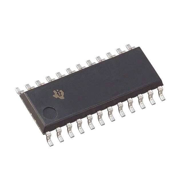
SN74BCT2827CDW
ACTIVE
SOIC
DW
24
25
RoHS & Green
NIPDAU
Level-1-260C-UNLIM
0 to 70
BCT2827C
(1)
The marketing status values are defined as follows:
ACTIVE: Product device recommended for new designs.
LIFEBUY: TI has announced that the device will be discontinued, and a lifetime-buy period is in effect.
NRND: Not recommended for new designs. Device is in production to support existing customers, but TI does not recommend using this part in a new design.
PREVIEW: Device has been announced but is not in production. Samples may or may not be available.
OBSOLETE: TI has discontinued the production of the device.
(2)
RoHS: TI defines "RoHS" to mean semiconductor products that are compliant with the current EU RoHS requirements for all 10 RoHS substances, including the requirement that RoHS substance
do not exceed 0.1% by weight in homogeneous materials. Where designed to be soldered at high temperatures, "RoHS" products are suitable for use in specified lead-free processes. TI may
reference these types of products as "Pb-Free".
RoHS Exempt: TI defines "RoHS Exempt" to mean products that contain lead but are compliant with EU RoHS pursuant to a specific EU RoHS exemption.
Green: TI defines "Green" to mean the content of Chlorine (Cl) and Bromine (Br) based flame retardants meet JS709B low halogen requirements of


 工商网监
湘ICP备2023018690号
工商网监
湘ICP备2023018690号
