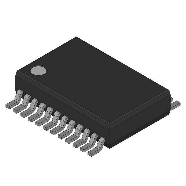
Product
Folder
Sample &
Buy
Technical
Documents
Support &
Community
Tools &
Software
SN74CBT3383, SN54CBT3383
SCDS003P – NOVEMBER 1992 – REVISED DECEMBER 2015
SNx4CBT3383 10-Bit Bus-Exchange Switch
1 Features
•
•
1
•
•
•
•
•
3 Description
High-Bandwidth Data Path (Up to 200 MHz)
Low and Flat ON-State Resistance (rON)
Characteristics Over Operating Range
(rON = 5 Ω Typical)
Control Inputs Can Be Driven by TTL or 5-V and
3.3-V CMOS Outputs
Bidirectional Data Flow With Near-Zero
Propagation Delay
Low Input and Output Capacitance Minimizes
Loading and Signal Distortion (Cio(OFF) = 6 pF
Typical)
VCC Operating Range From 4.5 V to 5 V
Low Power Consumption (ICC = 50 µA Maximum)
2 Applications
•
•
•
•
•
Enterprise Servers
Ethernet Switches
Routers
Servers
Industrial PCs
The SN74CBT3383 and SN54CBT3383 devices
provide ten bits of high-speed TTL-compatible
bus switching or exchanging. The low ON-state
resistance of the switch allows connections to be
made with minimal propagation delay.
The devices operate as a 10-bit bus switch or a
5-bit bus exchanger, which provides swapping of
the A and B pairs of signals. The bus-exchange
function is selected when BX is high. The
switches are connected when BE is low.
Device Information(1)
PART NUMBER
PACKAGE
BODY SIZE (NOM)
SN74CBT3383DB
SSOP (24)
8.40 mm × 5.30 mm
SN74CBT3383DBQ
SSOP (24)
8.65 mm × 3.90 mm
SN74CBT3383DW
SOIC (24)
15.40 mm × 7.50 mm
SN74CBT3383PW
TSSOP (24)
7.80 mm × 4.40 mm
SNJ54CBT3383JT
CDIP (24)
32.00 mm × 6.92 mm
SN54CBT3383W
CFP (24)
14.35 × 9.08 mm
(1) For all available packages, see the orderable addendum at
the end of the data sheet.
Logic Diagram (Positive Logic)
3
1A1
4
1A2
5A1
21
22
5A2
BE
BX
2
5
20
23
1B1
1B2
5B1
5B2
1
13
1
An IMPORTANT NOTICE at the end of this data sheet addresses availability, warranty, changes, use in safety-critical applications,
intellectual property matters and other important disclaimers. PRODUCTION DATA.
On products compliant to MIL-PRF-38535, all parameters are
tested unless otherwise noted. On all other products, production
�SN74CBT3383, SN54CBT3383
SCDS003P – NOVEMBER 1992 – REVISED DECEMBER 2015
www.ti.com
Table of Contents
1
2
3
4
5
6
7
8
Features ..................................................................
Applications ...........................................................
Description .............................................................
Revision History.....................................................
Pin Configuration and Functions .........................
Specifications.........................................................
1
1
1
2
3
4
6.1
6.2
6.3
6.4
6.5
6.6
6.7
4
4
4
4
5
5
5
Absolute Maximum Ratings ......................................
ESD Ratings ............................................................
Recommended Operating Conditions.......................
Thermal Information ..................................................
Electrical Characteristics...........................................
Switching Characteristics ..........................................
Typical Characteristics ..............................................
Parameter Measurement Information .................. 6
Detailed Description .............................................. 7
8.1 Overview ................................................................... 7
8.2 Functional Block Diagram ......................................... 7
8.3 Feature Description................................................... 8
8.4 Device Functional Modes.......................................... 8
9
Application and Implementation .......................... 9
9.1 Application Information.............................................. 9
9.2 Typical Application ................................................... 9
10 Power Supply Recommendations ..................... 11
11 Layout................................................................... 11
11.1 Layout Guidelines ................................................. 11
11.2 Layout Example .................................................... 11
12 Device and Documentation Support ................. 12
12.1
12.2
12.3
12.4
12.5
12.6
Documentation Support .......................................
Related Links ........................................................
Community Resources..........................................
Trademarks ...........................................................
Electrostatic Discharge Caution ............................
Glossary ................................................................
12
12
12
12
12
12
13 Mechanical, Packaging, and Orderable
Information ........................................................... 12
4 Revision History
NOTE: Page numbers for previous revisions may differ from page numbers in the current version.
Changes from Revision O (July 2004) to Revision P
•
2
Page
Added Pin Configuration and Functions, Specifications, ESD Ratings, Detailed Description, Application and
Implementation, Power Supply Recommendations, Layout, Device and Documentation Support, and Mechanical,
Packaging, and Orderable Information................................................................................................................................... 1
Submit Documentation Feedback
Copyright © 1992–2015, Texas Instruments Incorporated
Product Folder Links: SN74CBT3383 SN54CBT3383
�SN74CBT3383, SN54CBT3383
www.ti.com
SCDS003P – NOVEMBER 1992 – REVISED DECEMBER 2015
5 Pin Configuration and Functions
DB, DBQ, DW, JT, W, or PW Package
24-Pin SSOP, SOIC, CDIP, CFP, or TSSOP
Top View
__
BE
1
24
1B1
2
23
5B2
1A1
3
22
5A2
1A2
4
21
5A1
1B2
5
20
5B1
2B1
6
19
4B2
2A1
7
18
4A2
2A2
8
17
4A1
2B2
9
16
4B1
3B1
10
15
3B2
3A1
11
14
3A2
GND
12
13
BX
VCC
Pin Functions
PIN
NO.
NAME
I/O
DESCRIPTION
1
BE
I
2
1B1
I/O
Active-low input enable pin
Transceiver I/O pin
3
1A1
I/O
Transceiver I/O pin
4
1A2
I/O
Transceiver I/O pin
5
1B2
I/O
Transceiver I/O pin
6
2B1
I/O
Transceiver I/O pin
7
2A1
I/O
Transceiver I/O pin
8
2A2
I/O
Transceiver I/O pin
9
2B2
I/O
Transceiver I/O pin
10
3B1
I/O
Transceiver I/O pin
11
3A1
I/O
Transceiver I/O pin
12
GND
—
Ground
13
BX
I
14
3A2
I/O
Transceiver I/O pin
15
3B2
I/O
Transceiver I/O pin
16
4B1
I/O
Transceiver I/O pin
17
4A1
I/O
Transceiver I/O pin
18
4A2
I/O
Transceiver I/O pin
19
4B2
I/O
Transceiver I/O pin
20
5B1
I/O
Transceiver I/O pin
21
5A1
I/O
Transceiver I/O pin
22
5A2
I/O
Transceiver I/O pin
23
5B2
I/O
Transceiver I/O pin
24
VCC
—
Power pin
Output select pin
Copyright © 1992–2015, Texas Instruments Incorporated
Product Folder Links: SN74CBT3383 SN54CBT3383
Submit Documentation Feedback
3
�SN74CBT3383, SN54CBT3383
SCDS003P – NOVEMBER 1992 – REVISED DECEMBER 2015
www.ti.com
6 Specifications
6.1 Absolute Maximum Ratings
over operating free-air temperature range (unless otherwise noted) (1)
VCC
MIN
MAX
UNIT
Supply voltage
–0.5
7
V
(2)
–0.5
VI
Input voltage
7
V
IO
Continuos channel current
128
mA
IIK
Input clamp current (VI/O
很抱歉,暂时无法提供与“SN74CBT3383DBQR”相匹配的价格&库存,您可以联系我们找货
免费人工找货- 国内价格
- 1+14.60160
- 10+12.77640
- 30+11.63160
