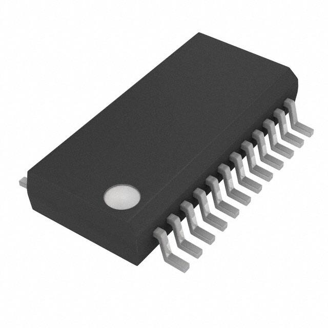
Product
Folder
Order
Now
Technical
Documents
Support &
Community
Tools &
Software
SN74CBTLV3383
SCDS047H – MARCH 1998 – REVISED DECEMBER 2018
SN74CBTLV3383 Low-Voltage 10-Bit FET Bus-Exchange Switch
1 Features
3 Description
•
•
•
•
The SN74CBTLV3383 provides ten bits of high-speed
bus switching or exchanging. The low on-state
resistance of the switch allows connections to be
made with minimal propagation delay.
1
•
5-Ω Switch Connection Between Two Ports
Rail-to-Rail Switching on Data I/O Ports
Ioff Supports Partial-Power-Down Mode Operation
Latch-Up Performance Exceeds 250 mA Per
JESD 17
ESD Protection Exceeds JESD 22
– 2000-V Human-Body Model (A114-A
– 200-V Machine Model (A115-A)
2 Applications
•
•
•
Gaming
Rack Server
Communication Board
The device operates as a 10-bit bus switch or as a 5bit bus exchanger, which provides swapping of the A
and B pairs of signals. The bus-exchange function is
selected when BX is high, and BE is low.
This device is fully specified for partial-power-down
applications using Ioff. The Ioff feature ensures that
damaging current will not backflow through the device
when it is powered down. The device has isolation
during power off.
Device Information(1)
PART NUMBER
SN74CBTLV3383
PACKAGE
BODY SIZE (NOM)
QSOP − DBQ
8.65 mm x 3.90 mm
SOIC − DW
15.4 mm x 7.50 mm
TSSOP − PW
7.80 mm x 4.40 mm
TVSOP − DGV
5.00 mm x 4.40 mm
(1) For all available packages, see the orderable addendum at
the end of the data sheet.
spacer
spacer
spacer
Simplified Schematic, Each FET Switch
1
An IMPORTANT NOTICE at the end of this data sheet addresses availability, warranty, changes, use in safety-critical applications,
intellectual property matters and other important disclaimers. PRODUCTION DATA.
�SN74CBTLV3383
SCDS047H – MARCH 1998 – REVISED DECEMBER 2018
www.ti.com
Table of Contents
1
2
3
4
5
6
7
8
Features ..................................................................
Applications ...........................................................
Description .............................................................
Revision History.....................................................
Pin Configuration and Functions .........................
Specifications.........................................................
1
1
1
2
3
4
6.1
6.2
6.3
6.4
6.5
6.6
4
4
4
4
5
5
Absolute Maximum Ratings ......................................
ESD Ratings..............................................................
Recommended Operating Conditions.......................
Thermal Information ..................................................
Electrical Characteristics...........................................
Switching Characteristics ..........................................
Parameter Measurement Information .................. 6
Detailed Description .............................................. 7
8.1 Overview ................................................................... 7
8.2 Functional Block Diagram ......................................... 7
8.3 Feature Description................................................... 7
8.4 Device Functional Modes.......................................... 8
9
Application and Implementation .......................... 9
9.1 Application Information.............................................. 9
9.2 Typical Application ................................................... 9
10 Power Supply Recommendations ..................... 10
11 Layout................................................................... 11
11.1 Layout Guidelines ................................................. 11
11.2 Layout Example .................................................... 11
12 Device and Documentation Support ................. 12
12.1
12.2
12.3
12.4
12.5
12.6
Documentation Support ........................................
Receiving Notification of Documentation Updates
Community Resources..........................................
Trademarks ...........................................................
Electrostatic Discharge Caution ............................
Glossary ................................................................
12
12
12
12
12
12
13 Mechanical, Packaging, and Orderable
Information ........................................................... 12
4 Revision History
NOTE: Page numbers for previous revisions may differ from page numbers in the current version.
Changes from Revision G (October 2003) to Revision H
•
2
Page
Added Device Information table, ESD Ratings table, Feature Description section, Device Functional Modes,
Application and Implementation section, Power Supply Recommendations section, Layout section, Device and
Documentation Support section, and Mechanical, Packaging, and Orderable Information section. .................................... 1
Submit Documentation Feedback
Copyright © 1998–2018, Texas Instruments Incorporated
Product Folder Links: SN74CBTLV3383
�SN74CBTLV3383
www.ti.com
SCDS047H – MARCH 1998 – REVISED DECEMBER 2018
5 Pin Configuration and Functions
DBQ, DGV, DW, OR PW Package
24-Pin
Top View
BE
1
24
VCC
1B1
2
23
5B2
1A1
3
22
5A2
1A2
4
21
5A1
1B2
5
20
5B1
2B1
6
19
4B2
2A1
7
18
4A2
2A2
8
17
4A1
2B2
9
16
4B1
3B1
10
15
3B2
3A1
11
14
3A2
GND
12
13
BX
Not to scale
Pin Functions
PIN
NAME
NO.
I/O
DESCRIPTION
Active low enable: When this pin is high, all switches are turned off. When this pin is low, BX pin controls
the signal path selection.
BE
1
I
1B1
2
I/O
Signal path. Can be an input or output
1A1
3
I/O
Signal path. Can be an input or output
1A2
4
I/O
Signal path. Can be an input or output
1B2
5
I/O
Signal path. Can be an input or output
2B1
6
I/O
Signal path. Can be an input or output
2A1
7
I/O
Signal path. Can be an input or output
2A2
8
I/O
Signal path. Can be an input or output
2B2
9
I/O
Signal path. Can be an input or output
3B1
10
I/O
Signal path. Can be an input or output
3A1
11
I/O
Signal path. Can be an input or output
GND
12
P
Ground (0V) reference
BX
13
I
Controls state of switches
3A2
14
I/O
Signal path. Can be an input or output
3B2
15
I/O
Signal path. Can be an input or output
4B1
16
I/O
Signal path. Can be an input or output
4A1
17
I/O
Signal path. Can be an input or output
4A2
18
I/O
Signal path. Can be an input or output
4B2
19
I/O
Signal path. Can be an input or output
5B1
20
I/O
Signal path. Can be an input or output
5A1
21
I/O
Signal path. Can be an input or output
5A2
22
I/O
Signal path. Can be an input or output
5B2
23
I/O
Signal path. Can be an input or output
VCC
24
P
Positive power supply.
Submit Documentation Feedback
Copyright © 1998–2018, Texas Instruments Incorporated
Product Folder Links: SN74CBTLV3383
3
�SN74CBTLV3383
SCDS047H – MARCH 1998 – REVISED DECEMBER 2018
www.ti.com
6 Specifications
6.1 Absolute Maximum Ratings
over operating free-air temperature range (unless otherwise noted) (1)
MIN
MAX
VCC
Supply voltage range
–0.5
4.6
VI
Input voltage range
–0.5
UNIT
V
4.6
V
Continuous channel current .
128
mA
IIK
Input clamp current, VI/O < 0
–50
mA
Tstg
Storage temperature
150
°C
(1)
–65
Stresses beyond those listed under Absolute Maximum Ratings may cause permanent damage to the device. These are stress ratings
only, which do not imply functional operation of the device at these or any other conditions beyond those indicated under Recommended
Operating Conditions. Exposure to absolute-maximum-rated conditions for extended periods may affect device reliability.
6.2 ESD Ratings
VALUE
Human-body model (HBM), per ANSI/ESDA/JEDEC JS-001
V(ESD)
(1)
(2)
Electrostatic discharge
(1)
UNIT
±2000
Charged-device model (CDM), per JEDEC specification JESD22C101 (2)
V
±1000
JEDEC document JEP155 states that 500-V HBM allows safe manufacturing with a standard ESD control process.
JEDEC document JEP157 states that 250-V CDM allows safe manufacturing with a standard ESD control process.
6.3 Recommended Operating Conditions (1)
over operating free-air temperature range (unless otherwise noted)
MIN
VCC
Supply voltage
VIH
MAX
2.3
High-level control input voltage
VIL
Low-level control input voltage
TA
Operating free-air temperature
(1)
NOM
VCC = 2.3 V to 2.7 V
1.7
VCC = 2.7 V to 3.6 V
2
3.6
UNIT
V
V
V
VCC = 2.3 V to 2.7 V
0.7
VCC = 2.7 V to 3.6 V
V
0.8
V
85
°C
–40
All unused control inputs of the device must be held at VCC or GND to ensure proper device operation. Refer to the TI application report,
Implications of Slow or Floating CMOS Inputs.
6.4 Thermal Information
SN74CBTLV3383
THERMAL METRIC
(1)
DBQ
(QSOP)
DVG
(TVSOP)
DW
(SPIC)
PW
(TSSOP)
24 PINS
24 PINS
24 PINS
24 PINS
UNIT
RθJA
Junction-to-ambient thermal resistance
86.6
105.6
66.6
90.1
°C/W
RθJC(top)
Junction-to-case (top) thermal resistance
40.5
36.9
36.7
34.12
°C/W
RθJB
Junction-to-board thermal resistance
40.8
51.1
36.6
45.2
°C/W
ψJT
Junction-to-top characterization parameter
7.8
2.6
13.1
2.8
°C/W
ψJB
Junction-to-board characterization parameter
40.4
50.6
36.4
44.8
°C/W
RθJC(bot)
Junction-to-case (bottom) thermal resistance
n/a
n/a
n/a
n/a
°C/W
(1)
4
For more information about traditional and new thermal metrics, see the Semiconductor and IC Package Thermal Metrics application
report.
Submit Documentation Feedback
Copyright © 1998–2018, Texas Instruments Incorporated
Product Folder Links: SN74CBTLV3383
�SN74CBTLV3383
www.ti.com
SCDS047H – MARCH 1998 – REVISED DECEMBER 2018
6.5 Electrical Characteristics
over operating free-air temperature range (unless otherwise noted)
PARAMETER
TEST CONDITIONS
VIK
Clamp current
VCC = 3 V
II = –18 mA
II
Input current
VCC = 3.6 V
VI = VCC or GND
Ioff
Partial power down mode
operation
VCC = 0 V
Supply current
MIN
TYP (1)
MAX
UNIT
–1.2
V
1
µA
VI or VIO = 0 to 3.6 V
10
µA
VCC = 3.6
IO = 0, VI = VCC or GND
10
µA
Supply current - Control inputs
VCC = 3.6 V
One input at
3V
300
µA
CI
Input Capacitance - Control
inputs
VI = 3 V or 0
CIO(OFF)
Input to output capacitance
VO = 3 V or 0
ICC
ΔICC
(2)
VCC = 2.3 V
TYP at VCC =
2.5 V
r(on) (3)
On-state resistance
VCC = 3 V
Other inputs at
VCC or GND
3.5
BE = VCC
VI = 0
VI = 1.7 V
VI = 0
pF
13.5
II = 64 mA
VI = 2.4 V
(1)
(2)
(3)
–1
5
pF
8
Ω
II = 24 mA
5
8
Ω
II = 15 mA
27
40
Ω
II = 64 mA
5
7
Ω
II = 24 mA
5
7
Ω
II = 15 mA
10
15
Ω
All typical values are at VCC = 3.3 V (unless otherwise noted), TA = 25°C
This is the increase in supply current for each input that is at the specified voltage level, rather than VCC or GND.
Measured by the voltage drop between the A and B terminals at the indicated current through the switch. On-state resistance is
determined by the lower of the voltages of the two (A or B) terminals.
6.6 Switching Characteristics
over operating free-air temperature range (unless otherwise noted)
PARAMETER
tpd
(1)
TEST CONDITIONS
FROM (INPUT)
TO (OUTPUT)
VCC = 2.5 V ± 0.2 V
MIN
MAX
VCC = 3.3 V ± 0.3 V
MIN
UNIT
Propagation delay time
A or B
Bo or A
0.25
ns
tpd
Propagation delay time
BX
A or B
1.5
5.8
1.5
4.7
ns
ten
Enable time
BE
A or B
1.5
5.3
1.5
4.7
ns
tdis
Disable time
BE
A or B
1
6
1
6
ns
(1)
0.15
MAX
The propagation delay is the calculated RC time constant of the typical on-state resistance of the switch and the specified load
capacitance, when driven by an ideal voltage source (zero output impedance).
Submit Documentation Feedback
Copyright © 1998–2018, Texas Instruments Incorporated
Product Folder Links: SN74CBTLV3383
5
�SN74CBTLV3383
SCDS047H – MARCH 1998 – REVISED DECEMBER 2018
www.ti.com
7 Parameter Measurement Information
Figure 1. Load Current
Figure 2. Voltage Waveforms Pulse Duration
xx
Figure 3. Voltage Waveforms Setup and Hold
Times
Figure 4. Voltage Waveforms Propagation Delay
Times Inverting and Noninverting Outputs
Figure 5. Voltage Waveforms Enable And Disable
Times Low- and High-Level Enabling
Notes:
A. CL includes probe and jig capacitance.
B. Waveform 1 is for an output with internal conditions such that the output is low except when disabled by the
output control. Waveform 2 is for an output with internal conditions such that the output is high except when
disabled by the output control
C. All input pulses are supplied by generators having the following characteristics: PRR ≤ 10 MHz, ZO = 50 Ω, tr
≤ 2 ns, tf ≤ 2 ns.
D. The outputs are measured one at a time with one transition per measurement.
E. tPLZ and tPHZ are the same as tdis.
F. tPZL and tPZH are the same as ten.
G. tPLH and tPHL are the same as tpd.
H. H. All parameters and waveforms are not applicable to all devices.
6
Submit Documentation Feedback
Copyright © 1998–2018, Texas Instruments Incorporated
Product Folder Links: SN74CBTLV3383
�SN74CBTLV3383
www.ti.com
SCDS047H – MARCH 1998 – REVISED DECEMBER 2018
8 Detailed Description
8.1 Overview
The SN74CBTLV3383 device is a 10-bit high-speed bus exchange FET switch. The low ONstate resistance of
the switch allows connections to be made with minimal propagation delay. The select (BX) input controls the data
flow. The FET multiplexers and demultiplexers are disabled when the output-enable (BE) input is high. This
device is fully specified for partial-power-down applications using Ioff. The Ioff feature ensures that damaging
current will not backflow through the device when it is powered down. The device has isolation during power off.
To ensure the high-impedance state during power up or power down, OE should be tied to VCC through a pullup
resistor; the minimum value of the resistor is determined by the current-sinking capability of the driver.
8.2 Functional Block Diagram
8.3 Feature Description
Bidirectional Operation
The SN74CBTLV3383 conducts equally well from source (xA1, xA2) to drain (xB1,xB2). Each channel has very
similar characteristics in both directions and supports both analog and digital signals.
Rail-to-rail switching
The SN74CBTLV3383 will support signals on the I/O path across the full supply range 0 to VCC
Submit Documentation Feedback
Copyright © 1998–2018, Texas Instruments Incorporated
Product Folder Links: SN74CBTLV3383
7
�SN74CBTLV3383
SCDS047H – MARCH 1998 – REVISED DECEMBER 2018
www.ti.com
8.4 Device Functional Modes
Shows the functional modes of the SN74CBTLV3383.
Table 1. Function Table
INPUTS
8
INPUTS–OUTPUTS
BE
BX
1A1–5A1
1A2-5A2
L
L
1B1–5B1
1B2–5B2
L
H
1B2–5B2
1B1–5B1
H
X
Z
Z
Submit Documentation Feedback
Copyright © 1998–2018, Texas Instruments Incorporated
Product Folder Links: SN74CBTLV3383
�SN74CBTLV3383
www.ti.com
SCDS047H – MARCH 1998 – REVISED DECEMBER 2018
9 Application and Implementation
NOTE
Information in the following applications sections is not part of the TI component
specification, and TI does not warrant its accuracy or completeness. TI’s customers are
responsible for determining suitability of components for their purposes. Customers should
validate and test their design implementation to confirm system functionality.
9.1 Application Information
The SN74CBTLV3383 device operates as a 10-bit bus switch or as a 5-bit bus exchanger, which provides
swapping of the A and B pairs of signals. The bus-exchange function is selected when BX is high, and BE is low.
The application shown here is a 5-bit bus being multiplexed between two devices. The BE and BX pins are used
to control the chip from the bus controller. This is a generic example, and could apply to many situations.
9.2 Typical Application
Figure 6. Simple Schematic
9.2.1 Design Requirements
1. Recommended Input Conditions:
– For specified high and low levels, see VIH and VIL in Recommended Operating Conditions.
– Inputs and outputs are overvoltage tolerant slowing them to go as high as 4.6 V at any valid VCC.
2. Recommended Output Conditions:
– Load currents should not exceed ±128 mA per channel.
3. Frequency Selection Criterion:
– Maximum frequency tested is 200 MHz.
9.2.2 Detailed Design Procedure
The SN74CBTLV3383 can be operated without any external components. All inputs signals passing through the
switch must fall within the recommend operating conditions of the SN74CBTLV3383 including signal range and
continuous current. For this design example, with a supply of 3.3 V, the signals can range from 0 V to 3.3 V
when the device is powered. The max continuous current can be 128 mA.
Submit Documentation Feedback
Copyright © 1998–2018, Texas Instruments Incorporated
Product Folder Links: SN74CBTLV3383
9
�SN74CBTLV3383
SCDS047H – MARCH 1998 – REVISED DECEMBER 2018
www.ti.com
10 Power Supply Recommendations
The SN74CBTLV3383 operates across a wide supply range of 2.3 V to 3.6 V. Do not exceed the absolute
maximum ratings because stresses beyond the listed ratings can cause permanent damage to the devices.
Power-supply bypassing improves noise margin and prevents switching noise propagation from the VDD supply
to other components. Good power-supply decoupling is important to achieve optimum performance. For
improved supply noise immunity, use a supply decoupling capacitor ranging from 0.1 μF to 10 μF from VDD to
ground. Place the bypass capacitors as close to the power supply pins of the device as possible using lowimpedance connections. TI recommends using multi-layer ceramic chip capacitors (MLCCs) that offer low
equivalent series resistance (ESR) and inductance (ESL) characteristics for power-supply decoupling purposes.
For very sensitive systems, or for systems in harsh noise environments, avoiding the use of vias for connecting
the capacitors to the device pins may offer superior noise immunity. The use of multiple vias in parallel lowers
the overall inductance and is beneficial for connections to ground planes.
10
Submit Documentation Feedback
Copyright © 1998–2018, Texas Instruments Incorporated
Product Folder Links: SN74CBTLV3383
�SN74CBTLV3383
www.ti.com
SCDS047H – MARCH 1998 – REVISED DECEMBER 2018
11 Layout
11.1 Layout Guidelines
Reflections and matching are closely related to the loop antenna theory but are different enough to be discussed
separately from the theory. When a PCB trace turns a corner at a 90° angle, a reflection can occur. A reflection
occurs primarily because of the change of width of the trace. At the apex of the turn, the trace width increases to
1.414 times the width. This increase upsets the transmission-line characteristics, especially the distributed
capacitance and self–inductance of the trace which results in the reflection. Not all PCB traces can be straight
and therefore some traces must turn corners. Figure 4 shows progressively better techniques of rounding
corners. Only the last example (BEST) maintains constant trace width and minimizes reflections.
11.2 Layout Example
BETTER
BEST
2W
WORST
1W min.
W
Figure 7. Example Layout
Submit Documentation Feedback
Copyright © 1998–2018, Texas Instruments Incorporated
Product Folder Links: SN74CBTLV3383
11
�SN74CBTLV3383
SCDS047H – MARCH 1998 – REVISED DECEMBER 2018
www.ti.com
12 Device and Documentation Support
12.1 Documentation Support
12.2 Receiving Notification of Documentation Updates
To receive notification of documentation updates, navigate to the device product folder on ti.com. In the upper
right corner, click on Alert me to register and receive a weekly digest of any product information that has
changed. For change details, review the revision history included in any revised document.
12.3 Community Resources
The following links connect to TI community resources. Linked contents are provided "AS IS" by the respective
contributors. They do not constitute TI specifications and do not necessarily reflect TI's views; see TI's Terms of
Use.
TI E2E™ Online Community TI's Engineer-to-Engineer (E2E) Community. Created to foster collaboration
among engineers. At e2e.ti.com, you can ask questions, share knowledge, explore ideas and help
solve problems with fellow engineers.
Design Support TI's Design Support Quickly find helpful E2E forums along with design support tools and
contact information for technical support.
12.4 Trademarks
E2E is a trademark of Texas Instruments.
All other trademarks are the property of their respective owners.
12.5 Electrostatic Discharge Caution
This integrated circuit can be damaged by ESD. Texas Instruments recommends that all integrated circuits be handled with
appropriate precautions. Failure to observe proper handling and installation procedures can cause damage.
ESD damage can range from subtle performance degradation to complete device failure. Precision integrated circuits may be more
susceptible to damage because very small parametric changes could cause the device not to meet its published specifications.
12.6 Glossary
SLYZ022 — TI Glossary.
This glossary lists and explains terms, acronyms, and definitions.
13 Mechanical, Packaging, and Orderable Information
The following pages include mechanical, packaging, and orderable information. This information is the most
current data available for the designated devices. This data is subject to change without notice and revision of
this document. For browser-based versions of this data sheet, refer to the left-hand navigation.
12
Submit Documentation Feedback
Copyright © 1998–2018, Texas Instruments Incorporated
Product Folder Links: SN74CBTLV3383
�PACKAGE OPTION ADDENDUM
www.ti.com
14-Oct-2022
PACKAGING INFORMATION
Orderable Device
Status
(1)
Package Type Package Pins Package
Drawing
Qty
Eco Plan
(2)
Lead finish/
Ball material
MSL Peak Temp
Op Temp (°C)
Device Marking
(3)
Samples
(4/5)
(6)
SN74CBTLV3383DBQR
ACTIVE
SSOP
DBQ
24
2500
RoHS & Green
NIPDAU
Level-2-260C-1 YEAR
-40 to 85
CBTLV3383
Samples
SN74CBTLV3383DGVR
ACTIVE
TVSOP
DGV
24
2000
RoHS & Green
NIPDAU
Level-1-260C-UNLIM
-40 to 85
CL383
Samples
SN74CBTLV3383DW
ACTIVE
SOIC
DW
24
25
RoHS & Green
NIPDAU
Level-1-260C-UNLIM
-40 to 85
CBTLV3383
Samples
SN74CBTLV3383DWE4
ACTIVE
SOIC
DW
24
25
RoHS & Green
NIPDAU
Level-1-260C-UNLIM
-40 to 85
CBTLV3383
Samples
SN74CBTLV3383DWR
ACTIVE
SOIC
DW
24
2000
RoHS & Green
NIPDAU
Level-1-260C-UNLIM
-40 to 85
CBTLV3383
Samples
SN74CBTLV3383PW
ACTIVE
TSSOP
PW
24
60
RoHS & Green
NIPDAU
Level-1-260C-UNLIM
-40 to 85
CL383
Samples
SN74CBTLV3383PWR
ACTIVE
TSSOP
PW
24
2000
RoHS & Green
NIPDAU
Level-1-260C-UNLIM
-40 to 85
CL383
Samples
(1)
The marketing status values are defined as follows:
ACTIVE: Product device recommended for new designs.
LIFEBUY: TI has announced that the device will be discontinued, and a lifetime-buy period is in effect.
NRND: Not recommended for new designs. Device is in production to support existing customers, but TI does not recommend using this part in a new design.
PREVIEW: Device has been announced but is not in production. Samples may or may not be available.
OBSOLETE: TI has discontinued the production of the device.
(2)
RoHS: TI defines "RoHS" to mean semiconductor products that are compliant with the current EU RoHS requirements for all 10 RoHS substances, including the requirement that RoHS substance
do not exceed 0.1% by weight in homogeneous materials. Where designed to be soldered at high temperatures, "RoHS" products are suitable for use in specified lead-free processes. TI may
reference these types of products as "Pb-Free".
RoHS Exempt: TI defines "RoHS Exempt" to mean products that contain lead but are compliant with EU RoHS pursuant to a specific EU RoHS exemption.
Green: TI defines "Green" to mean the content of Chlorine (Cl) and Bromine (Br) based flame retardants meet JS709B low halogen requirements of


 工商网监
湘ICP备2023018690号
工商网监
湘ICP备2023018690号
