Product
Folder
Order
Now
Technical
Documents
Support &
Community
Tools &
Software
SN74LVC1G08
SCES217Z – APRIL 1999 – REVISED MAY 2019
SN74LVC1G08 Single 2-Input Positive-AND Gate
1 Features
•
1
•
•
•
•
•
•
•
•
•
3 Description
2
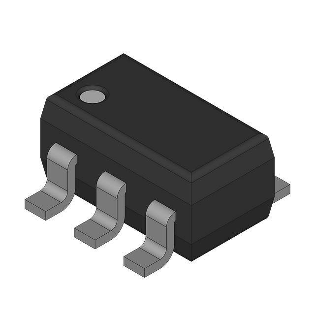
Available in the Ultra Small 0.64-mm
Package (DPW) With 0.5-mm Pitch
Supports 5-V VCC Operation
Inputs Accept Voltages to 5.5 V
Provides Down Translation to VCC
Max tpd of 3.6 ns at 3.3 V
Low Power Consumption, 10-μA Max ICC
±24-mA Output Drive at 3.3 V
Ioff Supports Live Insertion, Partial-Power-Down
Mode, and Back Drive Protection
Latch-Up Performance Exceeds 100 mA
Per JESD 78, Class II
ESD Protection Exceeds JESD 22
– 2000-V Human-Body Model (A114-A)
– 200-V Machine Model (A115-A)
– 1000-V Charged-Device Model (C101)
2 Applications
•
•
•
•
•
•
•
•
•
•
•
•
•
•
•
•
•
•
•
ATCA Solutions
Active Noise Cancellation (ANC)
Barcode Scanner
Blood Pressure Monitor
CPAP Machine
Cable Solutions
DLP 3D Machine Vision, Hyperspectral Imaging,
Optical Networking, and Spectroscopy
E-Book
Embedded PC
Field Transmitter: Temperature or Pressure
Sensor
Fingerprint Biometrics
HVAC: Heating, Ventilating, and Air Conditioning
Network-Attached Storage (NAS)
Server Motherboard and PSU
Software Defined Radio (SDR)
TV: High-Definition (HDTV), LCD, and Digital
Video Communications System
Wireless Data Access Card, Headset, Keyboard,
Mouse, and LAN Card
X-ray: Baggage Scanner, Medical, and Dental
This single 2-input positive-AND gate is designed for
1.65-V to 5.5-V VCC operation.
The SN74LVC1G08 device performs the Boolean
function or Y = A • B or Y = A + B in positive logic.
The CMOS device has high output drive while
maintaining low static power dissipation over a broad
VCC operating range.
The SN74LVC1G08 is available in a variety of
packages, including the ultra-small DPW package
with a body size of 0.8 mm × 0.8 mm.
white space
white space
Device Information(1)
DEVICE NAME
SN74LVC1G08
PACKAGE
BODY SIZE
SOT-23 (5)
2.9mm × 1.6mm
SC70 (5)
2.0mm × 1.25mm
X2SON (4)
0.8mm × 0.8mm
SON (6)
1.45mm × 1.0mm
SON (6)
1.0mm × 1.0mm
(1) For all available packages, see the orderable addendum at
the end of the datasheet.
1
An IMPORTANT NOTICE at the end of this data sheet addresses availability, warranty, changes, use in safety-critical applications,
intellectual property matters and other important disclaimers. PRODUCTION DATA.
�SN74LVC1G08
SCES217Z – APRIL 1999 – REVISED MAY 2019
www.ti.com
Table of Contents
1
2
3
4
5
6
7
Features ..................................................................
Applications ...........................................................
Description .............................................................
Revision History.....................................................
Pin Configuration and Functions .........................
Specifications.........................................................
1
1
1
2
3
4
6.1
6.2
6.3
6.4
6.5
6.6
6.7
6.8
6.9
6.10
4
4
5
5
6
6
6
7
7
7
Absolute Maximum Ratings .....................................
ESD Ratings..............................................................
Recommended Operating Conditions ......................
Thermal Information ..................................................
Electrical Characteristics...........................................
Switching Characteristics, CL = 15 pF ......................
Switching Characteristics, 1.8 V and 2.5 V ..............
Switching Characteristics, 3.3 V and 5 V .................
Operating Characteristics..........................................
Typical Characteristics ............................................
Parameter Measurement Information .................. 8
8
Detailed Description ............................................ 10
8.1
8.2
8.3
8.4
9
Overview .................................................................
Functional Block Diagram .......................................
Feature Description.................................................
Device Functional Modes........................................
10
10
10
10
Application and Implementation ........................ 11
9.1 Application Information............................................ 11
9.2 Typical Application ................................................. 11
10 Power Supply Recommendations ..................... 12
11 Layout................................................................... 12
11.1 Layout Guidelines ................................................. 12
11.2 Layout Example .................................................... 12
12 Device and Documentation Support ................. 13
12.1 Trademarks ........................................................... 13
12.2 Electrostatic Discharge Caution ............................ 13
12.3 Glossary ................................................................ 13
13 Mechanical, Packaging, and Orderable
Information ........................................................... 13
4 Revision History
Changes from Revision Y (April 2014) to Revision Z
Page
•
Added TJ(max) spec to Absolute Maximum Ratings table ..................................................................................................... 4
•
Moved Tstg spec from Handling Ratings table to Absolute Maximum Ratings table. ............................................................. 4
•
Renamed Handling Ratings table to ESD Ratings table ....................................................................................................... 4
Changes from Revision X (March 2014) to Revision Y
Page
•
Updated Handling Ratings table. ........................................................................................................................................... 4
•
Added Thermal Information table. ......................................................................................................................................... 5
•
Added Typical Characteristics. .............................................................................................................................................. 7
•
Added Detailed Description section. .................................................................................................................................... 10
•
Added Application and Implementation section. ................................................................................................................. 11
•
Added Power Supply Recommendations section. .............................................................................................................. 12
•
Added Layout section. ......................................................................................................................................................... 12
Changes from Revision W (July 2013) to Revision X
Page
•
Added Applications. ................................................................................................................................................................ 1
•
Added Device Information table. ............................................................................................................................................ 1
•
Moved Tstg to Handling Ratings table. .................................................................................................................................... 4
Changes from Revision V (November 2012) to Revision W
•
2
Page
Added parameter values for –40 to 125°C temperature ratings............................................................................................. 6
Submit Documentation Feedback
Copyright © 1999–2019, Texas Instruments Incorporated
Product Folder Links: SN74LVC1G08
�SN74LVC1G08
www.ti.com
SCES217Z – APRIL 1999 – REVISED MAY 2019
5 Pin Configuration and Functions
DBV PACKAGE
(TOP VIEW)
A
1
B
2
GND
3
DRL PACKAGE
(TOP VIEW)
DCK PACKAGE
(TOP VIEW)
A
VCC
5
5
1
B
2
GND
3
VCC
A
B
Y
4
B
A
1
5
3
2
4
3
4
Y
A
1
6
VCC
B
GND
2
5
3
4
NC
Y
Y
DPW PACKAGE
(TOP VIEW)
GND
VCC
2
GND
4
5
1
DSF PACKAGE
(TOP VIEW)
VCC
Y
YZP PACKAGE
(BOTTOM VIEW)
GND
3 4
B
2
A
1 5
Y
VCC
DRY PACKAGE
(TOP VIEW)
A
1
6
VCC
B
2
5
NC
GND
3
4
Y
NC – No internal connection
See mechanical drawings for dimensions.
Pin Functions
PIN
DESCRIPTION
NAME
DBV, DCK,
DRL, YZP
DRY, DSF
DPW
A
1
1
2
Input
B
2
2
1
Input
GND
3
3
3
Ground
Y
4
4
4
Output
VCC
5
6
5
Power pin
NC
5
Not connected
Submit Documentation Feedback
Copyright © 1999–2019, Texas Instruments Incorporated
Product Folder Links: SN74LVC1G08
3
�SN74LVC1G08
SCES217Z – APRIL 1999 – REVISED MAY 2019
www.ti.com
6 Specifications
6.1 Absolute Maximum Ratings (1)
over operating free-air temperature range (unless otherwise noted)
VCC
MIN
MAX
Supply voltage range
–0.5
6.5
UNIT
V
(2)
VI
Input voltage range
–0.5
6.5
V
VO
Voltage range applied to any output in the high-impedance or power-off state (2)
–0.5
6.5
V
VO
Voltage range applied to any output in the high or low state (2) (3)
–0.5
VCC + 0.5
V
IIK
Input clamp current
VI < 0
–50
mA
IOK
Output clamp current
VO < 0
–50
mA
IO
Continuous output current
±50
mA
±100
mA
150
°C
150
°C
Continuous current through VCC or GND
TJ(max) Junction temperature
Tstg
(1)
(2)
(3)
Storage temperature
–65
Stresses beyond those listed under Absolute Maximum Ratings may cause permanent damage to the device. These are stress ratings
only, and functional operation of the device at these or any other conditions beyond those indicated under Recommended Operating
Conditions is not implied. Exposure to absolute-maximum-rated conditions for extended periods may affect device reliability.
The input and output negative-voltage ratings may be exceeded if the input and output current ratings are observed.
The value of VCC is provided in the Recommended Operating Conditions table.
6.2 ESD Ratings
MIN
V(ESD)
(1)
(2)
4
Electrostatic discharge
MAX
Human body model (HBM), per ANSI/ESDA/JEDEC JS-001, all
pins (1)
0
2000
Charged device model (CDM), per JEDEC specification
JESD22-C101, all pins (2)
0
1000
UNIT
V
JEDEC document JEP155 states that 500-V HBM allows safe manufacturing with a standard ESD control process.
JEDEC document JEP157 states that 250-V CDM allows safe manufacturing with a standard ESD control process.
Submit Documentation Feedback
Copyright © 1999–2019, Texas Instruments Incorporated
Product Folder Links: SN74LVC1G08
�SN74LVC1G08
www.ti.com
SCES217Z – APRIL 1999 – REVISED MAY 2019
6.3 Recommended Operating Conditions (1)
VCC
Operating
Supply voltage
MAX
5.5
Data retention only
1.5
VCC = 1.65 V to 1.95 V
VIH
MIN
1.65
V
0.65 × VCC
VCC = 2.3 V to 2.7 V
High-level input voltage
UNIT
1.7
VCC = 3 V to 3.6 V
V
2
VCC = 4.5 V to 5.5 V
0.7 × VCC
VCC = 1.65 V to 1.95 V
0.35 × VCC
VCC = 2.3 V to 2.7 V
0.7
VCC = 3 V to 3.6 V
0.8
VIL
Low-level input voltage
VI
Input voltage
0
5.5
V
VO
Output voltage
0
VCC
V
VCC = 4.5 V to 5.5 V
0.3 × VCC
VCC = 1.65 V
–4
VCC = 2.3 V
IOH
High-level output current
–8
–16
VCC = 3 V
Low-level output current
Δt/Δv
–32
VCC = 1.65 V
4
VCC = 2.3 V
8
16
VCC = 3 V
Input transition rise or fall rate
(1)
mA
24
VCC = 4.5 V
32
VCC = 1.8 V ± 0.15 V, 2.5 V ± 0.2 V
20
VCC = 3.3 V ± 0.3 V
10
VCC = 5 V ± 0.5 V
TA
mA
–24
VCC = 4.5 V
IOL
V
ns/V
5
Operating free-air temperature
–40
125
°C
All unused inputs of the device must be held at VCC or GND to ensure proper device operation. Refer to the TI application report,
Implications of Slow or Floating CMOS Inputs, literature number SCBA004.
6.4 Thermal Information
SN74LVC1G08
THERMAL METRIC (1)
DBV
DCK
DRL
DRY
YZP
DPW
5 PINS
5 PINS
5 PINS
6 PINS
5 PINS
4 PINS
UNIT
RθJA
Junction-to-ambient thermal resistance
207.6
283.1
242.9
438.8
130
340
°C/W
RθJCtop
Junction-to-case (top) thermal resistance
145.2
92.3
77.5
276.8
54
215
°C/W
RθJB
Junction-to-board thermal resistance
53.5
60.9
77.5
271.7
51
294
°C/W
ψJT
Junction-to-top characterization parameter
37.5
1.7
9.6
83.8
1
41
°C/W
ψJB
Junction-to-board characterization parameter
53.1
60.1
77.3
271.4
50
294
°C/W
RθJCbot
Junction-to-case (bottom) thermal resistance
–
–
–
–
–
250
°C/W
(1)
For more information about traditional and new thermal metrics, see the Semiconductor and IC package thermal metrics application
report
Submit Documentation Feedback
Copyright © 1999–2019, Texas Instruments Incorporated
Product Folder Links: SN74LVC1G08
5
�SN74LVC1G08
SCES217Z – APRIL 1999 – REVISED MAY 2019
www.ti.com
6.5 Electrical Characteristics
over recommended operating free-air temperature range (unless otherwise noted)
PARAMETER
TEST CONDITIONS
TYP (1)
MIN
IOH = –100 μA
VOH
1.65 V to 5.5 V
VCC – 0.1
VCC – 0.15
1.2
1.2
IOH = –8 mA
2.3 V
1.9
1.9
2.4
2.4
2.3
2.3
3V
MAX
V
4.5 V
IOL = 100 μA
1.65 V to 5.5 V
0.1
0.1
IOL = 4 mA
1.65 V
0.45
0.45
IOL = 8 mA
2.3 V
0.3
0.3
3.8
0.4
0.4
0.55
0.55
0.55
0.55
0 to 5.5 V
±5
±5
μA
3V
IOL = 24 mA
IOL = 32 mA
4.5 V
VI = 5.5 V or GND
Ioff
VI or VO = 5.5 V
ICC
VI = 5.5 V or GND,
ΔICC
One input at VCC – 0.6 V,
Other inputs at VC C or GND
Ci
VI = VCC or GND
(1)
3.8
UNIT
TYP
IOH = –32 mA
IOL = 16 mA
II
MIN
1.65 V
IOH = –24 mA
A or B
inputs
MAX
IOH = –4 mA
IOH = –16 mA
VOL
–40°C to 125°C
RECOMMENDED
–40°C to 85°C
VCC
IO = 0
V
0
±10
±10
μA
1.65 V to 5.5 V
10
10
μA
3 V to 5.5 V
500
500
μA
3.3 V
4
4
pF
All typical values are at VCC = 3.3 V, TA = 25°C.
6.6 Switching Characteristics, CL = 15 pF
over recommended operating free-air temperature range (unless otherwise noted) (see Figure 3)
–40°C to 85°C
PARAMETER
FROM
(INPUT)
TO
(OUTPUT)
tpd
A or B
Y
VCC = 1.8 V
± 0.15 V
VCC = 2.5 V
± 0.2 V
VCC = 3.3 V
± 0.3 V
VCC = 5 V
± 0.5 V
MIN
MAX
MIN
MAX
MIN
MAX
MIN
MAX
1.5
7.2
0.7
4.4
0.8
3.6
0.8
3.4
UNIT
ns
6.7 Switching Characteristics, 1.8 V and 2.5 V (1)
over recommended operating free-air temperature range, (unless otherwise noted) (see Figure 4)
–40°C to 125°C
–40°C to 85°C
(1)
6
PARAMETER
FROM
(INPUT)
TO
(OUTPUT)
tpd
A or B
Y
RECOMMENDED
VCC = 1.8 V
± 0.15 V
VCC = 1.8 V
± 0.15 V
–40°C to 125°C
–40°C to 85°C
RECOMMENDED
VCC = 2.5 V
± 0.2 V
UNIT
VCC = 2.5 V
± 0.2 V
MIN
MAX
MIN
MAX
MIN
MAX
MIN
MAX
2.4
8
2.4
10
1.1
5.5
1.1
7
ns
On products compliant to MIL-PRF-38535, this parameter is not production tested.
Submit Documentation Feedback
Copyright © 1999–2019, Texas Instruments Incorporated
Product Folder Links: SN74LVC1G08
�SN74LVC1G08
www.ti.com
SCES217Z – APRIL 1999 – REVISED MAY 2019
6.8 Switching Characteristics, 3.3 V and 5 V (1)
over recommended operating free-air temperature range, CL = 30 pF or 50 pF (unless otherwise noted) (see Figure 4)
–40°C to 125°C
–40°C to 85°C
(1)
PARAMETER
FROM
(INPUT)
TO
(OUTPUT)
tpd
A or B
Y
VCC = 3.3 V
± 0.3 V
–40°C to 125°C
–40°C to 85°C
RECOMMENDED
VCC = 3.3 V
± 0.3 V
RECOMMENDED
VCC = 5 V
± 0.5 V
UNIT
VCC = 5 V
± 0.5 V
MIN
MAX
MIN
MAX
MIN
MAX
MIN
MAX
1
4.5
1
6
1
4
1
5
ns
On products compliant to MIL-PRF-38535, this parameter is not production tested.
6.9 Operating Characteristics
TA = 25°C
PARAMETER
Cpd
TEST
CONDITIONS
VCC = 1.8 V
VCC = 2.5 V
VCC = 3.3 V
VCC = 5 V
TYP
TYP
TYP
TYP
f = 10 MHz
21
24
26
31
Power dissipation capacitance
UNIT
pF
6.10 Typical Characteristics
8
6
TPD
7
5
6
TPD - ns
TPD - ns
4
3
5
4
3
2
2
1
1
TPD
0
-100
0
-50
0
50
Temperature - °C
100
150
0
1
D001
Figure 1. TPD Across Temperature at 3.3V Vcc
2
3
Vcc - V
4
5
Product Folder Links: SN74LVC1G08
D002
Figure 2. TPD Across Vcc at 25°C
Submit Documentation Feedback
Copyright © 1999–2019, Texas Instruments Incorporated
6
7
�SN74LVC1G08
SCES217Z – APRIL 1999 – REVISED MAY 2019
www.ti.com
7 Parameter Measurement Information
VLOAD
S1
RL
From Output
Under Test
Open
TEST
GND
CL
(see Note A)
S1
Open
VLOAD
tPLH/tPHL
tPLZ/tPZL
tPHZ/tPZH
RL
GND
LOAD CIRCUIT
INPUTS
VCC
1.8 V ± 0.15 V
2.5 V ± 0.2 V
3.3 V ± 0.3 V
5 V ± 0.5 V
VI
tr/tf
VCC
VCC
3V
VCC
£2 ns
£2 ns
£2.5 ns
£2.5 ns
VM
VLOAD
CL
RL
VD
VCC/2
VCC/2
1.5 V
VCC/2
2 × VCC
2 × VCC
6V
2 × VCC
15 pF
15 pF
15 pF
15 pF
1 MW
1 MW
1 MW
1 MW
0.15 V
0.15 V
0.3 V
0.3 V
VI
Timing Input
VM
0V
tW
tsu
VI
Input
VM
VM
th
VI
Data Input
VM
VM
0V
0V
VOLTAGE WAVEFORMS
PULSE DURATION
VOLTAGE WAVEFORMS
SETUP AND HOLD TIMES
VI
VM
Input
VM
0V
tPLH
VOH
VM
VOL
tPHL
tPLZ
VLOAD/2
VM
tPZH
VM
VM
VM
0V
Output
Waveform 1
S1 at VLOAD
(see Note B)
tPLH
VOH
Output
VM
tPZL
tPHL
VM
Output
VI
Output
Control
VOL
VOLTAGE WAVEFORMS
PROPAGATION DELAY TIMES
INVERTING AND NONINVERTING OUTPUTS
Output
Waveform 2
S1 at GND
(see Note B)
VOL + VD
VOL
tPHZ
VM
VOH – VD
VOH
»0 V
VOLTAGE WAVEFORMS
ENABLE AND DISABLE TIMES
LOW- AND HIGH-LEVEL ENABLING
NOTES: A. CL includes probe and jig capacitance.
B. Waveform 1 is for an output with internal conditions such that the output is low, except when disabled by the output control.
Waveform 2 is for an output with internal conditions such that the output is high, except when disabled by the output control.
C. All input pulses are supplied by generators having the following characteristics: PRR £ 10 MHz, ZO = 50 W.
D. The outputs are measured one at a time, with one transition per measurement.
E. tPLZ and tPHZ are the same as tdis.
F. tPZL and tPZH are the same as ten.
G. tPLH and tPHL are the same as tpd.
H. All parameters and waveforms are not applicable to all devices.
Figure 3. Load Circuit and Voltage Waveforms
8
Submit Documentation Feedback
Copyright © 1999–2019, Texas Instruments Incorporated
Product Folder Links: SN74LVC1G08
�SN74LVC1G08
www.ti.com
SCES217Z – APRIL 1999 – REVISED MAY 2019
Parameter Measurement Information (continued)
VLOAD
S1
RL
From Output
Under Test
Open
TEST
GND
CL
(see Note A)
S1
Open
VLOAD
tPLH/tPHL
tPLZ/tPZL
tPHZ/tPZH
RL
GND
LOAD CIRCUIT
INPUTS
VCC
1.8 V ± 0.15 V
2.5 V ± 0.2 V
3.3 V ± 0.3 V
5 V ± 0.5 V
VI
tr/tf
VCC
VCC
3V
VCC
£2 ns
£2 ns
£2.5 ns
£2.5 ns
VM
VLOAD
CL
RL
VD
VCC/2
VCC/2
1.5 V
VCC/2
2 × VCC
2 × VCC
6V
2 × VCC
30 pF
30 pF
50 pF
50 pF
1 kW
500 W
500 W
500 W
0.15 V
0.15 V
0.3 V
0.3 V
VI
Timing Input
VM
0V
tW
tsu
VI
Input
VM
VM
th
VI
Data Input
VM
VM
0V
0V
VOLTAGE WAVEFORMS
PULSE DURATION
VOLTAGE WAVEFORMS
SETUP AND HOLD TIMES
VI
VM
Input
VM
0V
tPLH
VOH
Output
VM
VOL
tPHL
VM
VM
0V
tPLZ
Output
Waveform 1
S1 at VLOAD
(see Note B)
tPLH
VLOAD/2
VM
tPZH
VOH
Output
VM
tPZL
tPHL
VM
VI
Output
Control
VM
VOL
VOLTAGE WAVEFORMS
PROPAGATION DELAY TIMES
INVERTING AND NONINVERTING OUTPUTS
Output
Waveform 2
S1 at GND
(see Note B)
VOL + VD
VOL
tPHZ
VM
VOH – VD
VOH
»0 V
VOLTAGE WAVEFORMS
ENABLE AND DISABLE TIMES
LOW- AND HIGH-LEVEL ENABLING
NOTES: A. CL includes probe and jig capacitance.
B. Waveform 1 is for an output with internal conditions such that the output is low, except when disabled by the output control.
Waveform 2 is for an output with internal conditions such that the output is high, except when disabled by the output control.
C. All input pulses are supplied by generators having the following characteristics: PRR £ 10 MHz, ZO = 50 W.
D. The outputs are measured one at a time, with one transition per measurement.
E. tPLZ and tPHZ are the same as tdis.
F. tPZL and tPZH are the same as ten.
G. tPLH and tPHL are the same as tpd.
H. All parameters and waveforms are not applicable to all devices.
Figure 4. Load Circuit and Voltage Waveforms
Submit Documentation Feedback
Copyright © 1999–2019, Texas Instruments Incorporated
Product Folder Links: SN74LVC1G08
9
�SN74LVC1G08
SCES217Z – APRIL 1999 – REVISED MAY 2019
www.ti.com
8 Detailed Description
8.1 Overview
The SN74LVC1G08 device contains one 2-input positive AND gate device and performs the Boolean function
Y = A • B or Y = A + B . This device is fully specified for partial-power-down applications using Ioff. The Ioff circuitry
disables the outputs, preventing damaging current backflow through the device when it is powered down.
The DPW package technology is a major breakthrough in IC packaging. Its tiny 0.64 mm square footprint saves
significant board space over other package options while still retaining the traditional manufacturing friendly lead
pitch of 0.5 mm.
8.2 Functional Block Diagram
8.3 Feature Description
•
•
•
•
Wide operating voltage range.
– Operates from 1.65 V to 5.5 V.
Allows down voltage translation.
Inputs accept voltages to 5.5 V.
Ioff feature allows voltages on the inputs and outputs when VCC is 0 V.
8.4 Device Functional Modes
Table 1. Function Table
INPUTS
10
A
B
OUTPUT
Y
H
H
H
L
X
L
X
L
L
Submit Documentation Feedback
Copyright © 1999–2019, Texas Instruments Incorporated
Product Folder Links: SN74LVC1G08
�SN74LVC1G08
www.ti.com
SCES217Z – APRIL 1999 – REVISED MAY 2019
9 Application and Implementation
9.1 Application Information
The SN74LVC1G08 is a high drive CMOS device that can be used for implementing AND logic with a high output
drive, such as an LED application. It can produce 24 mA of drive current at 3.3 V making it Ideal for driving
multiple outputs and good for high speed applications up to 100 MHz. The inputs are 5.5 V tolerant allowing it to
translate down to VCC.
9.2 Typical Application
AND Logic Function
Basic LED Driver
VCC
VCC
A- uC or Logic
A- uC or Logic
Y- uC or Logic
B- uC or Logic
LVC1G08
B- uC or Logic
LVC1G08
9.2.1 Design Requirements
This device uses CMOS technology and has balanced output drive. Care should be taken to avoid bus
contention because it can drive currents that would exceed maximum limits. The high drive will also create fast
edges into light loads so routing and load conditions should be considered to prevent ringing.
9.2.2 Detailed Design Procedure
1. Recommended Input Conditions
– Rise time and fall time specs. See (Δt/ΔV) in the Recommended Operating Conditions table.
– Specified high and low levels. See (VIH and VIL) in the Recommended Operating Conditions table.
– Inputs are overvoltage tolerant allowing them to go as high as (VI max) in the Recommended Operating
Conditions table at any valid VCC.
2. Recommend Output Conditions
– Load currents should not exceed (IO max) per output and should not exceed total current (continuous
current through VCC or GND) for the part. These limits are located in the Absolute Maximum Ratings
table.
– Outputs should not be pulled above VCC.
Submit Documentation Feedback
Copyright © 1999–2019, Texas Instruments Incorporated
Product Folder Links: SN74LVC1G08
11
�SN74LVC1G08
SCES217Z – APRIL 1999 – REVISED MAY 2019
www.ti.com
Typical Application (continued)
9.2.3 Application Curves
10
8
Icc
Icc
Icc
Icc
1.8V
2.5V
3.3V
5V
Icc - mA
6
4
2
0
-2
-20
0
20
40
Frequency - MHz
60
80
D003
Figure 5. Icc vs Frequency
10 Power Supply Recommendations
The power supply can be any voltage between the min and max supply voltage rating located in the
Recommended Operating Conditions table.
Each Vcc pin should have a good bypass capacitor to prevent power disturbance. For devices with a single
supply, a 0.1-μF capacitor is recommended and if there are multiple Vcc pins then 0.01-μF or 0.022-μF capacitor
is recommended for each power pin. It is ok to parallel multiple bypass capacitors to reject different frequencies
of noise. 0.1-μF and 1-μF capacitors are commonly used in parallel. The bypass capacitor should be installed as
close to the power pin as possible for best results.
11 Layout
11.1 Layout Guidelines
When using multiple bit logic devices inputs should not ever float. In many cases, functions or parts of functions
of digital logic devices are unused; for example, when only two inputs of a triple-input AND gate are used or only
3 of the 4 buffer gates are used. Such input pins should not be left unconnected because the undefined voltages
at the outside connections result in undefined operational states. Specified below are the rules that must be
observed under all circumstances. All unused inputs of digital logic devices must be connected to a high or low
bias to prevent them from floating. The logic level that should be applied to any particular unused input depends
on the function of the device. Generally they will be tied to Gnd or Vcc whichever make more sense or is more
convenient.
11.2 Layout Example
VCC
Unused Input
Input
Output
Unused Input
Output
Input
12
Submit Documentation Feedback
Copyright © 1999–2019, Texas Instruments Incorporated
Product Folder Links: SN74LVC1G08
�SN74LVC1G08
www.ti.com
SCES217Z – APRIL 1999 – REVISED MAY 2019
12 Device and Documentation Support
12.1 Trademarks
All trademarks are the property of their respective owners.
12.2 Electrostatic Discharge Caution
These devices have limited built-in ESD protection. The leads should be shorted together or the device placed in conductive foam
during storage or handling to prevent electrostatic damage to the MOS gates.
12.3 Glossary
SLYZ022 — TI Glossary.
This glossary lists and explains terms, acronyms, and definitions.
13 Mechanical, Packaging, and Orderable Information
The following pages include mechanical packaging and orderable information. This information is the most
current data available for the designated devices. This data is subject to change without notice and revision of
this document. For browser-based versions of this data sheet, refer to the left-hand navigation.
Submit Documentation Feedback
Copyright © 1999–2019, Texas Instruments Incorporated
Product Folder Links: SN74LVC1G08
13
�PACKAGE OPTION ADDENDUM
www.ti.com
10-Dec-2020
PACKAGING INFORMATION
Orderable Device
Status
(1)
Package Type Package Pins Package
Drawing
Qty
Eco Plan
(2)
Lead finish/
Ball material
MSL Peak Temp
Op Temp (°C)
Device Marking
(3)
(4/5)
(6)
SN74LVC1G08DBVR
ACTIVE
SOT-23
DBV
5
3000
RoHS & Green
NIPDAU | SN
Level-1-260C-UNLIM
-40 to 125
(C085, C08F, C08J,
C08K, C08R, C
08T)
(C08P, C08S)
SN74LVC1G08DBVRE4
ACTIVE
SOT-23
DBV
5
3000
RoHS & Green
NIPDAU
Level-1-260C-UNLIM
-40 to 125
C08
C08P
SN74LVC1G08DBVRG4
ACTIVE
SOT-23
DBV
5
3000
RoHS & Green
NIPDAU
Level-1-260C-UNLIM
SN74LVC1G08DBVT
ACTIVE
SOT-23
DBV
5
250
RoHS & Green
NIPDAU | SN
Level-1-260C-UNLIM
-40 to 125
(C085, C08F, C08J,
C08K, C08R)
(C08H, C08P, C08S)
SN74LVC1G08DBVTE4
ACTIVE
SOT-23
DBV
5
250
RoHS & Green
NIPDAU
Level-1-260C-UNLIM
-40 to 125
C08
C08P
SN74LVC1G08DCK3
ACTIVE
SC70
DCK
5
3000
RoHS &
Non-Green
SNBI
Level-1-260C-UNLIM
-40 to 125
(CEF, CEZ)
SN74LVC1G08DCKR
ACTIVE
SC70
DCK
5
3000
RoHS & Green
NIPDAU | SN
Level-1-260C-UNLIM
-40 to 125
(CE5, CEF, CEJ, CE
K, CER, CET)
(CEH, CEP, CES)
SN74LVC1G08DCKRE4
ACTIVE
SC70
DCK
5
3000
RoHS & Green
NIPDAU
Level-1-260C-UNLIM
-40 to 125
CE5
CES
SN74LVC1G08DCKRG4
ACTIVE
SC70
DCK
5
3000
RoHS & Green
NIPDAU
Level-1-260C-UNLIM
-40 to 125
CE5
CES
SN74LVC1G08DCKT
ACTIVE
SC70
DCK
5
250
RoHS & Green
NIPDAU | SN
Level-1-260C-UNLIM
-40 to 125
(CE5, CEF, CEJ, CE
K, CER, CET)
(CEH, CEP, CES)
SN74LVC1G08DCKTE4
ACTIVE
SC70
DCK
5
250
RoHS & Green
NIPDAU
Level-1-260C-UNLIM
-40 to 125
CE5
CES
SN74LVC1G08DCKTG4
ACTIVE
SC70
DCK
5
250
RoHS & Green
NIPDAU
Level-1-260C-UNLIM
-40 to 125
CE5
CES
SN74LVC1G08DPWR
ACTIVE
X2SON
DPW
5
3000
RoHS & Green
NIPDAU
Level-1-260C-UNLIM
-40 to 125
M4
SN74LVC1G08DRLR
ACTIVE
SOT-5X3
DRL
5
4000
RoHS & Green NIPDAU | NIPDAUAG
Level-1-260C-UNLIM
-40 to 125
(CE7, CER)
Addendum-Page 1
C08
C08P
Samples
�PACKAGE OPTION ADDENDUM
www.ti.com
Orderable Device
10-Dec-2020
Status
(1)
Package Type Package Pins Package
Drawing
Qty
Eco Plan
(2)
Lead finish/
Ball material
NIPDAUAG
MSL Peak Temp
Op Temp (°C)
Device Marking
(3)
(4/5)
(6)
SN74LVC1G08DRLRG4
ACTIVE
SOT-5X3
DRL
5
4000
RoHS & Green
Level-1-260C-UNLIM
-40 to 125
(CE7, CER)
SN74LVC1G08DRY2
ACTIVE
SON
DRY
6
5000
RoHS & Green NIPDAU | NIPDAUAG
Level-1-260C-UNLIM
-40 to 125
CE
SN74LVC1G08DRYR
ACTIVE
SON
DRY
6
5000
RoHS & Green
Level-1-260C-UNLIM
-40 to 125
CE
SN74LVC1G08DSF2
ACTIVE
SON
DSF
6
5000
RoHS & Green NIPDAU | NIPDAUAG
Level-1-260C-UNLIM
-40 to 125
CE
SN74LVC1G08DSFR
ACTIVE
SON
DSF
6
5000
RoHS & Green NIPDAU | NIPDAUAG
Level-1-260C-UNLIM
-40 to 125
CE
SN74LVC1G08YZPR
ACTIVE
DSBGA
YZP
5
3000
RoHS & Green
Level-1-260C-UNLIM
-40 to 85
(CE, CE7)
NIPDAU
SNAGCU
(1)
The marketing status values are defined as follows:
ACTIVE: Product device recommended for new designs.
LIFEBUY: TI has announced that the device will be discontinued, and a lifetime-buy period is in effect.
NRND: Not recommended for new designs. Device is in production to support existing customers, but TI does not recommend using this part in a new design.
PREVIEW: Device has been announced but is not in production. Samples may or may not be available.
OBSOLETE: TI has discontinued the production of the device.
(2)
RoHS: TI defines "RoHS" to mean semiconductor products that are compliant with the current EU RoHS requirements for all 10 RoHS substances, including the requirement that RoHS substance
do not exceed 0.1% by weight in homogeneous materials. Where designed to be soldered at high temperatures, "RoHS" products are suitable for use in specified lead-free processes. TI may
reference these types of products as "Pb-Free".
RoHS Exempt: TI defines "RoHS Exempt" to mean products that contain lead but are compliant with EU RoHS pursuant to a specific EU RoHS exemption.
Green: TI defines "Green" to mean the content of Chlorine (Cl) and Bromine (Br) based flame retardants meet JS709B low halogen requirements of


 工商网监
湘ICP备2023018690号
工商网监
湘ICP备2023018690号

