Product
Folder
Order
Now
Support &
Community
Tools &
Software
Technical
Documents
TCA9534A
SCPS198C – SEPTEMBER 2014 – REVISED FEBRUARY 2017
TCA9534A Low Voltage 8-Bit I2C and SMBUS Low-Power I/O Expander With Interrupt
Output and Configuration Registers
1 Features
3 Description
•
•
•
•
The TCA9534A is a 16-pin device that provides 8 bits
of general purpose parallel input and output (I/O)
expansion for the two-line bidirectional I2C bus (or
SMBus) protocol. The device can operate with a
power supply voltage ranging from 1.65 V to 5.5 V,
which allows for use with a wide range of devices.
The device supports both 100-kHz (Standard-mode)
and 400-kHz (Fast-mode) clock frequencies. I/O
expanders such as the TCA9534A provide a simple
solution when additional I/Os are needed for
switches, sensors, push-buttons, LEDs, fans, and
other similar devices.
1
•
•
•
•
•
•
•
•
•
•
•
•
Low Standby Current Consumption
I2C to Parallel Port Expander
Open-Drain Active-Low Interrupt Output
Operating Power-Supply Voltage Range of 1.65 V
to 5.5 V
5-V Tolerant I/O Ports
400-kHz Fast I2C Bus
Three Hardware Address Pins Allow up to Eight
Devices on the I2C/SMBus
Input and Output Configuration Register
Polarity Inversion Register
Internal Power-On Reset
Power-Up With All Channels Configured as Inputs
No Glitch on Power Up
Noise Filter on SCL/SDA Inputs
Latched Outputs With High-Current Drive
Maximum Capability for Directly Driving LEDs
Latch-Up Performance Exceeds 100 mA Per
JESD 78, Class II
ESD Protection Exceeds JESD 22
– 2000-V Human-Body Model (A114-A)
– 1000-V Charged-Device Model (C101)
The features of the TCA9534A include an interrupt
that is generated on the INT pin. This allows the
master to know when an input port changes state.
The A0, A1, and A2 hardware selectable address
pins allow up to eight TCA9534A devices on the
same I2C bus. The device can also be reset to its
default sate by cycling the power supply and causing
a power-on reset.
Device Information(1)
PART NUMBER
TCA9534A
PACKAGE
BODY SIZE (NOM)
TSSOP (16)
5.00 mm × 4.40 mm
SOIC (16)
10.30 mm × 7.50 mm
(1) For all available packages, see the orderable addendum at
the end of the datasheet.
2 Applications
•
•
•
•
•
•
Servers
Routers (Telecom Switching Equipment)
Personal Computers
Personal Electronics (for example: Gaming
Consoles)
Industrial Automation
Products With GPIO-Limited Processors
Simplified Schematic
VCC
I2C or SMBus
Master
SDA
SCL
INT
(e.g. Processor)
TCA9534A
A0
A1
A2
GND
P0
P1
P2
P3
P4
P5
P6
P7
Peripheral
Devices
• RESET,
ENABLE, or
control
inputs
• INT or
status
outputs
• LEDs
1
An IMPORTANT NOTICE at the end of this data sheet addresses availability, warranty, changes, use in safety-critical applications,
intellectual property matters and other important disclaimers. PRODUCTION DATA.
�TCA9534A
SCPS198C – SEPTEMBER 2014 – REVISED FEBRUARY 2017
www.ti.com
Table of Contents
1
2
3
4
5
6
7
8
Features ..................................................................
Applications ...........................................................
Description .............................................................
Revision History.....................................................
Pin Configuration and Functions .........................
Specifications.........................................................
1
1
1
2
4
5
6.1
6.2
6.3
6.4
6.5
6.6
6.7
6.8
5
5
5
6
6
7
8
9
Absolute Maximum Ratings .....................................
Handling Ratings.......................................................
Recommended Operating Conditions.......................
Thermal Information ..................................................
Electrical Characteristics...........................................
I2C Interface Timing Requirements...........................
Switching Characteristics ..........................................
Typical Characteristics ..............................................
Parameter Measurement Information ................ 12
Detailed Description ............................................ 15
8.1 Overview ................................................................. 15
8.2 Functional Block Diagram ....................................... 16
8.3 Feature Description................................................. 17
8.4 Device Functional Modes........................................ 17
8.5 Programming........................................................... 17
8.6 Register Maps ......................................................... 19
9
Application and Implementation ........................ 24
9.1 Application Information............................................ 24
9.2 Typical Application ................................................. 24
10 Power Supply Recommendations ..................... 27
10.1 Power-On Reset Requirements ........................... 27
11 Layout................................................................... 29
11.1 Layout Guidelines ................................................. 29
11.2 Layout Example .................................................... 29
12 Device and Documentation Support ................. 30
12.1
12.2
12.3
12.4
12.5
12.6
Related Documentation .......................................
Receiving Notification of Documentation Updates
Community Resources..........................................
Trademarks ...........................................................
Electrostatic Discharge Caution ............................
Glossary ................................................................
30
30
30
30
30
30
13 Mechanical, Packaging, and Orderable
Information ........................................................... 30
4 Revision History
NOTE: Page numbers for previous revisions may differ from page numbers in the current version.
Changes from Revision B (December 2016) to Revision C
Page
•
Updated Figure 20 ............................................................................................................................................................... 13
•
Updated address in Table 1 ................................................................................................................................................. 18
Changes from Revision A (September 2014) to Revision B
Page
•
Updated the Description section ............................................................................................................................................ 1
•
Added DW package................................................................................................................................................................ 1
•
Corrected ESD ratings to reflect ± ratings.............................................................................................................................. 5
•
VIH values, improved performance ........................................................................................................................................ 5
•
Made changes to IOL in the Recommended Operating Conditions table................................................................................ 5
•
Changed VPORR limits.............................................................................................................................................................. 6
•
Changed VOH at VCC = 1.65 V................................................................................................................................................. 6
•
Updated IOL in the Electrical Characteristics table.................................................................................................................. 6
•
Changed ICC in the Electrical Characteristics table ................................................................................................................ 7
•
Deleted ΔICC parameter from the Electrical Characteristics table .......................................................................................... 7
•
Increased the pin capacitance maximum, decreased typical ................................................................................................. 7
•
Updated graphs in Typical Characteristics section ................................................................................................................ 9
•
Updated Interrupt Output (INT) section ................................................................................................................................ 17
•
Added the Calculating Junction Temperature and Power Dissipation section..................................................................... 25
•
Updated parameter values in Table 8 ................................................................................................................................. 27
•
Added VCC_MV to Table 8 ..................................................................................................................................................... 27
•
Updated Figure 39 ............................................................................................................................................................... 27
2
Submit Documentation Feedback
Copyright © 2014–2017, Texas Instruments Incorporated
Product Folder Links: TCA9534A
�TCA9534A
www.ti.com
SCPS198C – SEPTEMBER 2014 – REVISED FEBRUARY 2017
Changes from Original (August 2014) to Revision A
•
Page
Initial release of full version .................................................................................................................................................... 1
Submit Documentation Feedback
Copyright © 2014–2017, Texas Instruments Incorporated
Product Folder Links: TCA9534A
3
�TCA9534A
SCPS198C – SEPTEMBER 2014 – REVISED FEBRUARY 2017
www.ti.com
5 Pin Configuration and Functions
PW and DW Package
16-Pin TSSOP and SOIC
Top View
A0
A1
A2
P0
P1
P2
P3
GND
1
16
2
15
3
14
4
13
5
12
6
11
7
10
8
9
VCC
SDA
SCL
INT
P7
P6
P5
P4
Pin Functions
PIN
NO.
NAME
I/O
DESCRIPTION
1
A0
I
Address input. Connect directly to VCC or ground
2
A1
I
Address input. Connect directly to VCC or ground
3
A2
I
Address input. Connect directly to VCC or ground
4
P0
I/O
P-port input-output. Push-pull design structure. At power on,
P0 is configured as an input
5
P1
I/O
P-port input-output. Push-pull design structure. At power on,
P1 is configured as an input
6
P2
I/O
P-port input-output. Push-pull design structure. At power on,
P2 is configured as an input
7
P3
I/O
P-port input-output. Push-pull design structure. At power on,
P3 is configured as an input
8
GND
—
Ground
9
P4
I/O
P-port input-output. Push-pull design structure. At power on,
P4 is configured as an input
10
P5
I/O
P-port input-output. Push-pull design structure. At power on,
P5 is configured as an input
11
P6
I/O
P-port input-output. Push-pull design structure. At power on,
P6 is configured as an input
12
P7
I/O
P-port input-output. Push-pull design structure. At power on,
P7 is configured as an input
13
INT
O
Interrupt output. Connect to VCC through a pull-up resistor
14
SCL
I
Serial clock bus. Connect to VCC through a pull-up resistor
15
SDA
I/O
Serial data bus. Connect to VCC through a pull-up resistor
16
VCC
—
Supply voltage
4
Submit Documentation Feedback
Copyright © 2014–2017, Texas Instruments Incorporated
Product Folder Links: TCA9534A
�TCA9534A
www.ti.com
SCPS198C – SEPTEMBER 2014 – REVISED FEBRUARY 2017
6 Specifications
6.1 Absolute Maximum Ratings (1)
over operating free-air temperature range (unless otherwise noted)
VCC
Supply voltage
(2)
MIN
MAX
UNIT
–0.5
6
V
–0.5
6
V
–0.5
6
V
VI
Input voltage
VO
Output voltage
IIK
Input clamp current
VI < 0
–20
mA
IOK
Output clamp current
VO < 0
–20
mA
IIOK
Input-output clamp current
VO < 0 or VO > VCC
±20
mA
IOL
Continuous output low current through a single P-port
VO = 0 to VCC
50
mA
IOH
Continuous output high current through a single P-port
VO = 0 to VCC
–50
mA
(2)
Continuous current through GND by all P-ports, INT, and SDA
250
Continuous current through VCC by all P-ports
–160
TJ(MAX)
Maximum junction temperature
100
°C
Tstg
Storage temperature
150
°C
ICC
(1)
(2)
–65
mA
Stresses beyond those listed under Absolute Maximum Ratings may cause permanent damage to the device. These are stress ratings
only, which do not imply functional operation of the device at these or any other conditions beyond those indicated under Recommended
Operating Conditions. Exposure to absolute-maximum-rated conditions for extended periods may affect device reliability.
The input negative-voltage and output voltage ratings may be exceeded if the input and output current ratings are observed.
6.2 Handling Ratings
VALUE
V(ESD)
(1)
(2)
Electrostatic
discharge
Human body model (HBM), per ANSI/ESDA/JEDEC JS-001, all pins (1)
±2000
Charged device model (CDM), per JEDEC specification JESD22-C101, all
pins (2)
±1000
UNIT
V
JEDEC document JEP155 states that 500-V HBM allows safe manufacturing with a standard ESD control process.
JEDEC document JEP157 states that 250-V CDM allows safe manufacturing with a standard ESD control process.
6.3 Recommended Operating Conditions
VCC
Supply voltage
VIH
High-level input voltage
VIL
Low-level input voltage
IOH
High-level output current
(1)
VCC = 1.65 V to 5.5 V
0.7 × VCC
VCC = 1.65 V to 2.7 V
0.7 × VCC
5.5
SCL, SDA
VCC = 1.65 V to 5.5 V
–0.5
0.3 × VCC
VCC = 1.65 V to 2.7 V
–0.5
0.3 × VCC
VCC = 3 V to 5.5 V
–0.5
0.2 × VCC
A0, A1, A2, P7–P0
Any P-port, P7–P0
INT, SDA
ICC
5.5
A0, A1, A2, P7–P0
Low-level output current (2)
Continuous current through
GND
MAX
SCL, SDA
P00-P07, P10-P17
IOL
MIN
1.65
–10
Tj ≤ 65°C
25
Tj ≤ 85°C
18
Tj ≤ 100°C
9
Tj ≤ 85°C
6
Tj ≤ 100°C
3
All P-ports P7-P0, INT, and SDA
200
Continuous current through VCC All P-ports P7-P0
TA
(1)
(2)
VCC
Operating free-air temperature
UNIT
V
V
V
mA
mA
mA
–80
–40
85
°C
The SCL and SDA pins shall not be at a higher potential than the supply voltage VCC in the application, or an increase in leakage
current, II, will result.
The values shown apply to specific junction temperatures. See the Calculating Junction Temperature and Power Dissipation section on
how to calculate the junction temperature.
Submit Documentation Feedback
Copyright © 2014–2017, Texas Instruments Incorporated
Product Folder Links: TCA9534A
5
�TCA9534A
SCPS198C – SEPTEMBER 2014 – REVISED FEBRUARY 2017
www.ti.com
6.4 Thermal Information
TCA9534A
THERMAL METRIC (1)
PW (TSSOP)
DW (SOIC)
16 PINS
16 PINS
UNIT
RθJA
Junction-to-ambient thermal resistance
122
92.2
°C/W
RθJC(top)
Junction-to-case (top) thermal resistance
56.4
53.8
°C/W
RθJB
Junction-to-board thermal resistance
67.1
56.9
°C/W
ψJT
Junction-to-top characterization parameter
10.8
26.4
°C/W
ψJB
Junction-to-board characterization parameter
66.5
56.4
°C/W
(1)
For more information about traditional and new thermal metrics, see the Semiconductor and IC Package Thermal Metrics application
report.
6.5 Electrical Characteristics
over operating free-air temperature range (unless otherwise noted)
PARAMETER
VIK
Input diode clamp voltage
TEST CONDITIONS
II = –18 mA
VPOR Power-on reset voltage, VCC
rising
R
VI = VCC or GND, IO = 0
VPOR Power-on reset voltage, VCC
falling
F
VI = VCC or GND, IO = 0
IOH = –8 mA
VOH
P-port high-level output
voltage (2)
IOH = –10 mA
SDA (3)
IOL
P port (4)
INT
II
(5)
SCL, SDA
A2–A0
VCC
MIN
1.65 V to 5.5 V
–1.2
TYP (1) MAX
V
1.2
0.75
1.65 V
1.2
2.3 V
1.8
3V
2.6
4.5 V
4.1
1.65 V
1
2.3 V
1.7
3V
2.5
4.5 V
4
VOL = 0.4 V
1.65 V to 5.5 V
3
VOL = 0.5 V
1.65 V to 5.5 V
8
VOL = 0.7 V
1.65 V to 5.5 V
10
VOL = 0.4 V
1.65 V to 5.5 V
3
VI = VCC or GND
1.65 V to 5.5 V
UNIT
1.5
1
V
V
V
mA
±1
±1
μA
IIH
P port
VI = VCC
1.65 V to 5.5 V
1
μA
IIL
P port
VI = GND
1.65 V to 5.5 V
–1
μA
(1)
(2)
(3)
(4)
(5)
6
All typical values are at nominal supply voltage (1.8-, 2.5-, 3.3-, or 5-V VCC) and TA = 25°C.
Each P-port I/O configured as a high output must be externally limited to a maximum of 10 mA, and the total current sourced by all I/Os
(P-ports P7-P0) through VCC must be limited to a maximum current of 80 mA.
The SDA pin must be externally limited to a maximum of 12 mA, and the total current sunk by all I/Os (P-ports P7-P0, INT, and SDA)
through GND must be limited to a maximum current of 200 mA.
Each P-port I/O configured as a low output must be externally limited to a maximum of 25 mA, and the total current sunk by all I/Os (Pports P7-P0, INT, and SDA) through GND must be limited to a maximum current of 200 mA.
The INT pin must be externally limited to a maximum of 7 mA, and the total current sunk by all I/Os (P-ports P7-P0, INT, and SDA)
through GND must be limited to a maximum current of 200 mA.
Submit Documentation Feedback
Copyright © 2014–2017, Texas Instruments Incorporated
Product Folder Links: TCA9534A
�TCA9534A
www.ti.com
SCPS198C – SEPTEMBER 2014 – REVISED FEBRUARY 2017
Electrical Characteristics (continued)
over operating free-air temperature range (unless otherwise noted)
PARAMETER
Operating mode
TEST CONDITIONS
VCC
VI = VCC or GND, IO = 0,
I/O = inputs, fscl = 400 kHz, no load
ICC
VI = VCC
Standby mode
VI = GND, IO = 0,
I/O = inputs, fscl = 0 kHz, no
load
VI = GND
Ci
Cio
SCL
SDA
P port
MIN
TYP (1) MAX
5.5 V
22
40
3.6 V
11
30
2.7 V
8
19
1.65
5
11
5.5 V
1.5
3.9
3.6 V
0.9
2.2
2.7 V
0.6
1.8
1.95 V
0.4
1.5
5.5 V
1.5
8.7
3.6 V
0.9
4
2.7 V
0.6
3
1.95 V
0.4
2.2
3
8
3
9.5
3.7
9.5
VI = VCC or GND
1.65 V to 5.5 V
VIO = VCC or GND
1.65 V to 5.5 V
UNIT
μA
pF
pF
6.6 I2C Interface Timing Requirements
over operating free-air temperature range (unless otherwise noted) (see Figure 19)
MIN
MAX
UNIT
100
kHz
STANDARD MODE
fscl
I2C clock frequency
0
tsch
I2C clock high time
4
2
tscl
I C clock low time
tsp
I2C spike time
tsds
I2C serial-data setup time
tsdh
I2C serial-data hold time
µs
4.7
µs
50
ns
250
ns
0
ns
2
ticr
I C input rise time
1000
ns
ticf
I2C input fall time
300
ns
tocf
I2C output fall time
300
ns
10-pF to 400-pF bus
2
tbuf
I C bus free time between stop and start
4.7
µs
tsts
I2C start or repeated start condition setup
4.7
µs
tsth
I2C start or repeated start condition hold
4
µs
2
tsps
I C stop condition setup
tvd(data)
Valid data time
SCL low to SDA output valid
4
3.45
µs
ns
tvd(ack)
Valid data time of ACK condition
ACK signal from SCL low to
SDA (out) low
3.45
µs
Cb
I2C bus capacitive load
400
pF
400
kHz
FAST MODE
fscl
I2C clock frequency
0
2
tsch
I C clock high time
0.6
tscl
I2C clock low time
1.3
tsp
I2C spike time
I C serial-data setup time
tsdh
I2C serial-data hold time
ticr
I2C input rise time
µs
50
2
tsds
µs
100
ns
0
20
ns
300
Submit Documentation Feedback
Copyright © 2014–2017, Texas Instruments Incorporated
Product Folder Links: TCA9534A
ns
ns
7
�TCA9534A
SCPS198C – SEPTEMBER 2014 – REVISED FEBRUARY 2017
www.ti.com
I2C Interface Timing Requirements (continued)
over operating free-air temperature range (unless otherwise noted) (see Figure 19)
MIN
MAX
UNIT
20 × (VDD /
5.5 V)
300
ns
20 × (VDD /
5.5 V)
300
ns
ticf
I2C input fall time
tocf
I2C output fall time
tbuf
I2C bus free time between stop and start
1.3
µs
tsts
I2C start or repeated start condition setup
0.6
µs
tsth
I2C start or repeated start condition hold
0.6
µs
10-pF to 400-pF bus
2
tsps
I C stop condition setup
tvd(data)
Valid data time
SCL low to SDA output valid
0.6
0.9
µs
ns
tvd(ack)
Valid data time of ACK condition
ACK signal from SCL low to
SDA (out) low
0.9
µs
Cb
I2C bus capacitive load
400
pF
6.7 Switching Characteristics
over operating free-air temperature range (unless otherwise noted) (see Figure 20 and Figure 21)
PARAMETER
FROM
(INPUT)
TO
(OUTPUT)
P port
INT
4
µs
SCL
INT
4
µs
350
ns
MIN
MAX
UNIT
STANDARD and FAST MODE
tiv
Interrupt valid time
tir
Interrupt reset delay time
tpv
Output data valid
SCL
P7–P0
tps
Input data setup time
P port
SCL
100
ns
tph
Input data hold time
P port
SCL
1
μs
8
Submit Documentation Feedback
Copyright © 2014–2017, Texas Instruments Incorporated
Product Folder Links: TCA9534A
�TCA9534A
www.ti.com
SCPS198C – SEPTEMBER 2014 – REVISED FEBRUARY 2017
6.8 Typical Characteristics
TA = 25°C (unless otherwise noted)
40
2.2
Vcc = 1.65 V
Vcc = 1.8 V
Vcc = 2.5 V
32
Vcc = 3.3 V
Vcc = 3.6 V
Vcc = 5 V
Vcc = 5.5V
28
24
20
16
12
8
4
-15
10
35
TA - Temperature (°C)
60
Vcc = 5.5V
1.6
1.4
1.2
1
0.8
0.6
0.2
-40
85
-15
D001
Figure 1. Supply Current vs Temperature for Different
Supply Voltage (VCC)
10
35
TA - Temperature (°C)
60
85
D002
Figure 2. Standby Supply Current vs Temperature for
Different Supply Voltage (VCC)
30
30
-40qC
25qC
85qC
-40qC
25qC
85qC
25
IOL - Sink Current (mA)
25
ICC - Supply Current (µA)
1.8
Vcc = 3.3 V
Vcc = 3.6 V
Vcc = 5 V
0.4
0
-40
20
15
10
5
20 VCC = 1.65 V
15
10
5
0
1.5
0
2
2.5
3
3.5
4
4.5
VCC - Supply Voltage (V)
5
5.5
0
0.1
D003
Figure 3. Supply Current vs Supply Voltage for Different
Temperature (TA)
0.2
0.3
0.4
0.5
VOL - Output Low Voltage (V)
0.6
0.7
D004
Figure 4. I/O Sink Current vs Output Low Voltage for
Different Temperature (TA) for VCC = 1.65 V
60
35
25
IOL - Sink Current (mA)
-40qC
25qC
85qC
30
IOL - Sink Current (mA)
Vcc = 1.65 V
Vcc = 1.8 V
Vcc = 2.5 V
2
ICC - Supply Current (µA)
ICC - Supply Current (µA)
36
VCC = 1.8 V
20
15
10
50
-40qC
25qC
85qC
40
VCC = 2.5 V
30
20
10
5
0
0
0
0.1
0.2
0.3
0.4
0.5
VOL - Output Low Voltage (V)
0.6
0.7
0
D005
Figure 5. I/O Sink Current vs Output Low Voltage for
Different Temperature (TA) for VCC = 1.8 V
0.1
0.2
0.3
0.4
0.5
VOL - Output Low Voltage (V)
0.6
0.7
D006
Figure 6. I/O Sink Current vs Output Low Voltage for
Different Temperature (TA) for VCC = 2.5 V
Submit Documentation Feedback
Copyright © 2014–2017, Texas Instruments Incorporated
Product Folder Links: TCA9534A
9
�TCA9534A
SCPS198C – SEPTEMBER 2014 – REVISED FEBRUARY 2017
www.ti.com
Typical Characteristics (continued)
TA = 25°C (unless otherwise noted)
80
70
-40qC
25qC
85qC
50
VCC = 3.3 V
40
30
20
10
60
VCC = 5 V
50
40
30
20
10
0
0
0
0.1
0.2
0.3
0.4
0.5
VOL - Output Low Voltage (V)
0.6
0
0.7
0.1
0.2
0.3
0.4
0.5
VOL - Output Low Voltage (V)
D007
Figure 7. I/O Sink Current vs Output Low Voltage for
Different Temperature (TA) for VCC = 3.3 V
0.6
0.7
D009
Figure 8. I/O Sink Current vs Output Low Voltage for
Different Temperature (TA) for VCC = 5 V
300
90
70
VOL - Output Low Voltage (V)
-40qC
25qC
85qC
80
IOL - Sink Current (mA)
-40qC
25qC
85qC
70
IOL - Sink Current (mA)
IOL - Sink Current (mA)
60
VCC = 5.5 V
60
50
40
30
20
1.8 V, 1 mA
1.8 V, 10 mA
3.3 V, 1mA
250
3.3 V, 10 mA
5 V, 1 mA
5 V, 10 mA
200
150
100
50
10
0
-40
0
0
0.1
0.2
0.3
0.4
0.5
VOL - Output Low Voltage (V)
0.6
0.7
Figure 9. I/O Sink Current vs Output Low Voltage for
Different Temperature (TA) for VCC = 5.5 V
60
85
D011
25
-40qC
25qC
85qC
IOH - Source Current (mA)
IOH - Source Current (mA)
10
35
TA - Temperature (°C)
Figure 10. II/O Low Voltage vs Temperature for Different VCC
and IOL
20
15
VCC = 1.65 V
10
5
-40qC
25qC
85qC
20
VCC = 1.8 V
15
10
5
0
0
0
0.1
0.2
0.3
0.4
0.5
VCC-VOH - Output High Voltage (V)
0.6
0.7
0
D012
Figure 11. I/O Source Current vs Output High Voltage for
Different Temperature (TA) for VCC = 1.65 V
10
-15
D010
0.1
0.2
0.3
0.4
0.5
VCC-VOH - Output High Voltage (V)
0.6
0.7
D013
Figure 12. I/O Source Current vs Output High Voltage for
Different Temperature (TA) for VCC = 1.8 V
Submit Documentation Feedback
Copyright © 2014–2017, Texas Instruments Incorporated
Product Folder Links: TCA9534A
�TCA9534A
www.ti.com
SCPS198C – SEPTEMBER 2014 – REVISED FEBRUARY 2017
Typical Characteristics (continued)
TA = 25°C (unless otherwise noted)
60
40
IOH - Source Current (mA)
35
IOH - Source Current (mA)
-40qC
25qC
85qC
30
VCC = 2.5 V
25
20
15
10
0
40
VCC = 3.3 V
30
20
0
0
0.1
0.2
0.3
0.4
0.5
VCC-VOH - Output High Voltage (V)
0.6
0.7
0
0.1
0.2
0.3
0.4
0.5
VCC-VOH - Output High Voltage (V)
D014
0.6
0.7
D015
Figure 13. I/O Source Current vs Output High Voltage for
Different Temperature (TA) for VCC = 2.5 V
Figure 14. I/O Source Current vs Output High Voltage for
Different Temperature (TA) for VCC = 3.3 V
70
80
-40qC
25qC
85qC
50
-40qC
25qC
85qC
70
IOH - Source Current (mA)
60
IOH - Source Current (mA)
-40qC
25qC
85qC
10
5
VCC = 5 V
40
30
20
10
60
VCC = 5.5 V
50
40
30
20
10
0
0
0
0.1
0.2
0.3
0.4
0.5
VCC-VOH - Output High Voltage (V)
0.6
0.7
0
D016
Figure 15. I/O Source Current vs Output High Voltage for
Different Temperature (TA) for VCC = 5 V
350
0.1
0.2
0.3
0.4
0.5
VCC-VOH - Output High Voltage (V)
0.6
0.7
D017
Figure 16. I/O Source Current vs Output High Voltage for
Different Temperature (TA) for VCC = 5.5 V
400
18
1.65 V, 10 mA
2.5 V, 10 mA
3.6 V, 10 mA
5 V, 10 mA
5.5 V, 10 mA
15
1.65 V
1.8 V
2.5 V
3.3 V
5V
5.5 V
300
Delta ICC (µA)
VCC-VOH - I/O High Voltage (mV)
50
250
200
150
9
6
3
100
50
-40
12
-15
10
35
TA - Temperature (°C)
60
85
0
-40
D018
Figure 17. VCC – VOH Voltage vs Temperature for Different
VCC
-15
10
35
TA - Temperature (°C)
60
85
D019
Figure 18. Δ ICC vs Temperature for Different VCC (VI = VCC –
0.6 V)
Submit Documentation Feedback
Copyright © 2014–2017, Texas Instruments Incorporated
Product Folder Links: TCA9534A
11
�TCA9534A
SCPS198C – SEPTEMBER 2014 – REVISED FEBRUARY 2017
www.ti.com
7 Parameter Measurement Information
VCC
R L = 1 kW
SDA
DUT
CL = 50 pF
(see Note A)
SDA LOAD CONFIGURATION
Three Bytes for Complete
Device Programming
Stop
Address
Start
Address
Condition Condition
Bit 7
Bit 6
(P)
(S)
(MSB)
R/W
Bit 0
(LSB)
Address
Bit 1
tscl
ACK
(A)
Data
Bit 07
(MSB)
Data
Bit 10
(LSB)
Stop
Condition
(P)
tsch
0.7 ´ VCC
SCL
0.3 ´ VCC
ticr
tPHL
ticf
tbuf
tsts
tPLH
tsp
0.7 ´ VCC
SDA
0.3 ´ VCC
ticf
ticr
tsth
tsdh
tsds
tsps
Repeat
Start
Condition
Start or
Repeat
Start
Condition
Stop
Condition
VOLTAGE WAVEFORMS
BYTE
DESCRIPTION
1
I C address
2, 3
P-port data
2
A.
CL includes probe and jig capacitance.
B.
All inputs are supplied by generators having the following characteristics: PRR ≤ 10 MHz, ZO = 50 Ω, tr/tf ≤ 30 ns.
C.
All parameters and waveforms are not applicable to all devices.
Figure 19. I2C Interface Load Circuit and Voltage Waveforms
12
Submit Documentation Feedback
Copyright © 2014–2017, Texas Instruments Incorporated
Product Folder Links: TCA9534A
�TCA9534A
www.ti.com
SCPS198C – SEPTEMBER 2014 – REVISED FEBRUARY 2017
Parameter Measurement Information (continued)
VCC
RL = 4.7 kΩ
INT
DUT
CL = 100 pF
(see Note A)
INTERRUPT LOAD CONFIGURA TION
ACK
From Slave
Start
Condition
8 Bits
(One Data Byte)
From Port
R/W
Slave Address
S
0
1
1
1 A2 A1 A0 1
A
1
2
3
4
A
5
6
7
8
Data 1
ACK
From Slave
Data From Port
A
Data 2
1
P
A
t ir
t ir
B
B
INT
A
t iv
t sps
A
Data
Into
Port
Address
Data 1
0.7 × VCC
INT
SCL
0.3 × VCC
Data 2
0.7 × VCC
R/W
t iv
A
0.3 × VCC
t ir
0.7 × VCC
Pn
0.7 × VCC
INT
0.3 × VCC
0.3 × VCC
View A−A
View B−B
A.
CL includes probe and jig capacitance.
B.
All inputs are supplied by generators having the following characteristics: PRR ≤ 10 MHz, ZO = 50 Ω, tr/tf ≤ 30 ns.
C.
All parameters and waveforms are not applicable to all devices.
Figure 20. Interrupt Load Circuit and Voltage Waveforms
Submit Documentation Feedback
Copyright © 2014–2017, Texas Instruments Incorporated
Product Folder Links: TCA9534A
13
�TCA9534A
SCPS198C – SEPTEMBER 2014 – REVISED FEBRUARY 2017
www.ti.com
Parameter Measurement Information (continued)
Pn
500 Ÿ
DUT
2 x VCC
CL = 50 pF
(see Note A)
500 Ÿ
P-PORT LOAD CONFIGURATION
SCL
0.7 x VCC
P0
A
P3
0.3 x VCC
Slave
ACK
SDA
tpv
(see Note B)
Unstable Data
Last Stable Bit
WRITE MODE (R/W = 0)
0.7 x VCC
SCL
P0
A
P3
0.3 x VCC
tph
tps
0.7 x VCC
Pn
0.3 x VCC
READ MODE (R/W = 1)
A.
CL includes probe and jig capacitance.
B.
tpv is measured from 0.7 × VCC on SCL to 50% I/O (Pn) output.
C.
All inputs are supplied by generators having the following characteristics: PRR ≤ 10 MHz, ZO = 50 Ω, tr/tf ≤ 30 ns.
D.
The outputs are measured one at a time, with one transition per measurement.
E.
All parameters and waveforms are not applicable to all devices.
Figure 21. P-Port Load Circuit and Voltage Waveforms
14
Submit Documentation Feedback
Copyright © 2014–2017, Texas Instruments Incorporated
Product Folder Links: TCA9534A
�TCA9534A
www.ti.com
SCPS198C – SEPTEMBER 2014 – REVISED FEBRUARY 2017
8 Detailed Description
8.1 Overview
The TCA9534A is an 8-bit I/O expander for the two-line bidirectional bus (I2C) is designed for 1.65-V to 5.5-V VCC
operation. It provides general-purpose remote I/O expansion for most micro-controller families via the I2C
interface (serial clock, SCL, and serial data, SDA, pins).
The TCA9534A open-drain interrupt (INT) output is activated when any input state differs from its corresponding
Input Port register state and is used to indicate to the system master that an input state has changed. The INT
pin can be connected to the interrupt input of a micro-controller. By sending an interrupt signal on this line, the
remote I/O can inform the micro-controller if there is incoming data on its ports without having to communicate
via the I2C bus. Thus, the TCA9534A can remain a simple slave device. The device outputs (latched) have highcurrent drive capability for directly driving LEDs.
Three hardware pins (A0, A1, and A2) are used to program and vary the fixed I2C slave address and allow up to
eight devices to share the same I2C bus or SMBus.
The system master can reset the TCA9534A in the event of a timeout or other improper operation by cycling the
power supply and causing a power-on reset (POR). A reset puts the registers in their default state and initializes
the I2C /SMBus state machine.
The TCA9534A consists of one 8-bit Configuration (input or output selection), Input Port, Output Port, and
Polarity Inversion (active high or active low) registers. At power on, the I/Os are configured as inputs. However,
the system master can enable the I/Os as either inputs or outputs by writing to the I/O configuration bits. The
data for each input or output is kept in the corresponding Input Port or Output Port register. The polarity of the
Input Port register can be inverted with the Polarity Inversion register. All registers can be read by the system
master.
The TCA9534A is identical to the TCA9554 except for the removal of the internal I/O pull-up resistors, which
greatly reduces power consumption when the I/Os are held LOW.
Submit Documentation Feedback
Copyright © 2014–2017, Texas Instruments Incorporated
Product Folder Links: TCA9534A
15
�TCA9534A
SCPS198C – SEPTEMBER 2014 – REVISED FEBRUARY 2017
www.ti.com
8.2 Functional Block Diagram
INT
A0
A1
A2
SCL
SDA
13
Interrupt
Logic
LP Filter
1
2
P7−P0
3
14
15
I2C Bus
Control
Input
Filter
Shift
Register
8 Bits
I/O
Port
Write Pulse
VCC
GND
16
8
Power-On
Reset
Read Pulse
Pin numbers shown are for the PW package.
Figure 22. Functional Block Diagram
Data From
Shift Register
Data From
Shift Register
Output Port
Register Data
VCC
Configuration
Register
Q1
D Q
FF
Write Configuration
Pulse
CK Q
Write Pulse
D Q
FF
P0 to P7
CK Q
Output Port
Register
Q2
Input Port
Register
Input Port
Register Data
D Q
FF
CK Q
Read Pulse
Data From Shift
Register
To INT
Polarity
Register Data
D Q
FF
CK Q
Write Polarity
Pulse
ESD Protection
Diode
GND
Polarity Inversion
Register
At power-on reset, all registers return to default values.
Figure 23. Simplified Schematic Of P0 To P7
16
Submit Documentation Feedback
Copyright © 2014–2017, Texas Instruments Incorporated
Product Folder Links: TCA9534A
�TCA9534A
www.ti.com
SCPS198C – SEPTEMBER 2014 – REVISED FEBRUARY 2017
8.3 Feature Description
8.3.1 I/O Port
When an I/O is configured as an input, FETs Q1 and Q2 are off, creating a high-impedance input. The input
voltage may be raised above VCC to a maximum of 5.5 V.
If the I/O is configured as an output, Q1 or Q2 is enabled depending on the state of the output port register. In
this case, there are low impedance paths between the I/O pin and either VCC or GND. The external voltage
applied to this I/O pin must not exceed the recommended levels for proper operation.
8.3.2 Interrupt Output (INT)
An interrupt is generated by any rising or falling edge of the port inputs in the input mode. After time, tiv, the
signal INT is valid. Resetting the interrupt circuit is achieved when data on the port is changed to the original
setting or data is read from the port that generated the interrupt. Resetting occurs in the read mode at the
acknowledge (ACK) bit after the rising edge of the SCL signal. Note that the INT is reset at the ACK just before
the byte of changed data is sent. Interrupts that occur during the ACK clock pulse can be lost (or be very short)
because of the resetting of the interrupt during this pulse. Each change of the I/Os after resetting is detected and
is transmitted as INT.
Reading from or writing to another device does not affect the interrupt circuit, and a pin configured as an output
cannot cause an interrupt. Changing an I/O from an output to an input may cause a false interrupt to occur if the
state of the pin does not match the contents of the Input Port register.
The INT output has an open-drain structure and requires pull-up resistor to VCC.
8.4 Device Functional Modes
8.4.1 Power-On Reset
When power (from 0 V) is applied to VCC, an internal power-on reset holds the TCA9534A in a reset condition
until VCC has reached VPORR. At that point, the reset condition is released and the TCA9534A registers and
SMBus/I2C state machine initialize to their default states. After that, VCC must be lowered to below VPORF and
then back up to the operating voltage for a power-on reset cycle.
8.5 Programming
8.5.1 I2C Interface
The TCA9534A has a standard bidirectional I2C interface that is controlled by a master device in order to be
configured or read the status of this device. Each slave on the I2C bus has a specific device address to
differentiate between other slave devices that are on the same I2C bus. Many slave devices require configuration
upon startup to set the behavior of the device. This is typically done when the master accesses internal register
maps of the slave, which have unique register addresses. A device can have one or multiple registers where
data is stored, written, or read. For more information see the Understanding the I2C Bus application report.
The physical I2C interface consists of the serial clock (SCL) and serial data (SDA) lines. Both SDA and SCL lines
must be connected to VCC through a pull-up resistor. The size of the pull-up resistor is determined by the amount
of capacitance on the I2C lines. For further details, see the I2C Pull-up Resistor Calculation application report.
Data transfer may be initiated only when the bus is idle. A bus is considered idle if both SDA and SCL lines are
high after a STOP condition.
Figure 24 and Figure 25 show the general procedure for a master to access a slave device:
1. If a master wants to send data to a slave:
– Master-transmitter sends a START condition and addresses the slave-receiver.
– Master-transmitter sends data to slave-receiver.
– Master-transmitter terminates the transfer with a STOP condition.
2. If a master wants to receive or read data from a slave:
– Master-receiver sends a START condition and addresses the slave-transmitter.
– Master-receiver sends the requested register to read to slave-transmitter.
– Master-receiver receives data from the slave-transmitter.
Submit Documentation Feedback
Copyright © 2014–2017, Texas Instruments Incorporated
Product Folder Links: TCA9534A
17
�TCA9534A
SCPS198C – SEPTEMBER 2014 – REVISED FEBRUARY 2017
www.ti.com
Programming (continued)
– Master-receiver terminates the transfer with a STOP condition.
SCL
SDA
Data Transfer
START
Condition
STOP
Condition
Figure 24. Definition of Start and Stop Conditions
SDA line stable while SCL line is high
SCL
1
0
1
0
1
0
1
0
ACK
MSB
Bit
Bit
Bit
Bit
Bit
Bit
LSB
ACK
SDA
Byte: 1010 1010 ( 0xAAh )
Figure 25. Bit Transfer
Table 1 shows the TCA9534A interface definition.
Table 1. Interface Definition Table
BYTE
2
I C slave address
Px I/O data bus
18
BIT
7 (MSB)
6
5
4
3
2
1
0 (LSB)
L
H
H
H
A2
A1
A0
R/W
P7
P6
P5
P4
P3
P2
P1
P0
Submit Documentation Feedback
Copyright © 2014–2017, Texas Instruments Incorporated
Product Folder Links: TCA9534A
�TCA9534A
www.ti.com
SCPS198C – SEPTEMBER 2014 – REVISED FEBRUARY 2017
8.6 Register Maps
8.6.1 Device Address
Figure 26 shows the address byte of the TCA9534A.
Slave Address
0
1
1
1
A2
A1
A0 R/W
Hardware
Selectable
Fixed
Figure 26. TCA9534A Address
Table 2 shows the TCA9534A address reference.
Table 2. Address Reference
INPUTS
I2C BUS SLAVE ADDRESS
A2
A1
A0
L
L
L
L
L
H
57 (decimal), 39 (hexadecimal)
L
H
L
58 (decimal), 3A (hexadecimal)
L
H
H
59 (decimal), 3B (hexadecimal)
H
L
L
60 (decimal), 3C (hexadecimal)
H
L
H
61 (decimal), 3D (hexadecimal)
H
H
L
62 (decimal), 3E (hexadecimal)
H
H
H
63 (decimal), 3F (hexadecimal)
56 (decimal), 38 (hexadecimal)
The last bit of the slave address defines the operation (read or write) to be performed. When it is high (1), a read
is selected, while a low (0) selects a write operation.
8.6.2 Control Register and Command Byte
Following the successful Acknowledgment of the address byte, the bus master sends a command byte that is
stored in the control register in the TCA9534A (see Figure 27). Two bits of this command byte state the operation
(read or write) and the internal register (input, output, polarity inversion or configuration) that is affected. This
register can be written or read through the I2C bus. The command byte is sent only during a write transmission.
Once a command byte has been sent, the register that was addressed continues to be accessed by reads until a
new command byte has been sent.
0
0
0
0
0
B2
B1
B0
Figure 27. Control Register Bits
Table 3 shows the TCA9534A command byte.
Table 3. Command Byte Table
CONTROL REGISTER BITS
B1
B0
COMMAND BYTE
(HEX)
0
0
0×00
0
1
0×01
1
0
0×02
1
1
0×03
REGISTER
PROTOCOL
POWER-UP DEFAULT
Input Port
Read byte
XXXX XXXX
Output Port
Read/write byte
1111 1111
Polarity Inversion
Read/write byte
0000 0000
Configuration
Read/write byte
1111 1111
Submit Documentation Feedback
Copyright © 2014–2017, Texas Instruments Incorporated
Product Folder Links: TCA9534A
19
�TCA9534A
SCPS198C – SEPTEMBER 2014 – REVISED FEBRUARY 2017
www.ti.com
8.6.3 Register Descriptions
The Input Port register (register 0) reflects the incoming logic levels of the pins, regardless of whether the pin is
defined as an input or an output by the Configuration register. It only acts on read operation. Writes to these
registers have no effect. The default value, X, is determined by the externally applied logic level. See Table 4.
Before a read operation, a write transmission is sent with the command byte to indicate to the I2C device that the
Input Port register is accessed next.
Table 4. Register 0 (Input Port Register) Table
BIT
I7
I6
I5
I4
I3
I2
I1
I0
DEFAULT
X
X
X
X
X
X
X
X
The Output Port register (register 1) shows the outgoing logic levels of the pins defined as outputs by the
Configuration register. Bit values in this register have no effect on pins defined as inputs. In turn, reads from this
register reflect the value that is in the flip-flop controlling the output selection, not the actual pin value. See
Table 5.
Table 5. Register 1 (Output Port Register) Table
BIT
O7
O6
O5
O4
O3
O2
O1
O0
DEFAULT
1
1
1
1
1
1
1
1
The Polarity Inversion register (register 2) allows polarity inversion of pins defined as inputs by the Configuration
register. If a bit in this register is set (written with 1), the corresponding port pin polarity is inverted. If a bit in this
register is cleared (written with a 0), the corresponding port pin original polarity is retained. See Table 6.
Table 6. Register 2 (Polarity Inversion Register) Table
BIT
N7
N6
N5
N4
N3
N2
N1
N0
DEFAULT
0
0
0
0
0
0
0
0
The Configuration register (register 3) configures the directions of the I/O pins. If a bit in this register is set to 1,
the corresponding port pin is enabled as an input with a high-impedance output driver. If a bit in this register is
cleared to 0, the corresponding port pin is enabled as an output. See Table 7.
Table 7. Register 3 (Configuration Register) Table
20
BIT
C7
C6
C5
C4
C3
C2
C1
C0
DEFAULT
1
1
1
1
1
1
1
1
Submit Documentation Feedback
Copyright © 2014–2017, Texas Instruments Incorporated
Product Folder Links: TCA9534A
�TCA9534A
www.ti.com
SCPS198C – SEPTEMBER 2014 – REVISED FEBRUARY 2017
8.6.3.1 Bus Transactions
Data is exchanged between the master and the TCA9534A through write and read commands.
8.6.3.1.1 Writes
To write on the I2C bus, the master sends a START condition on the bus with the address of the slave, as well
as the last bit (the R/W bit) set to 0, which signifies a write. After the slave sends the acknowledge bit, the master
then sends the register address of the register to which it wishes to write. The slave acknowledges again, letting
the master know it is ready. After this, the master starts sending the register data to the slave until the master
has sent all the data necessary (which is sometimes only a single byte), and the master terminates the
transmission with a STOP condition.
See Table 3 to see list of the internal registers and a description of each one.
Figure 28 shows an example of writing a single byte to a slave register.
Master controls SDA line
Slave controls SDA line
Write to one register in a device
Register Address N (8 bits)
Device (Slave) Address (7 bits)
S
0
1
1
1
A2 A1 A0
START
0
B7 B6 B5 B4 B3 B2 B1 B0
A
R/W=0
Data Byte to Register N (8 bits)
ACK
A
D7 D6 D5 D4 D3 D2 D1 D0
ACK
A
ACK
P
STOP
Figure 28. Write to Register
Figure 29 shows an example of writing to the output port register.
SCL
1
2
3
4
5
6
7
8
9
Slave Address
SDA
S
0
1
Command Byte
1 1 A2 A1 A
Start Condition
0
A
0
0
0
0
R/W ACK From Slave
0
0
Data to Port
0
1
A
Data 1
A
P
ACK From Slave
ACK From Slave
Write to Port
Data Out
From Port
Data 1 Valid
t pv
Figure 29. Write to Output Port Register
Figure 30 shows an example of writing to the configuration or polarity inversion registers.
Submit Documentation Feedback
Copyright © 2014–2017, Texas Instruments Incorporated
Product Folder Links: TCA9534A
21
�TCA9534A
SCPS198C – SEPTEMBER 2014 – REVISED FEBRUARY 2017
SCL
1
2
3
4
5
6
7
8
www.ti.com
9
Slave Address
SDA
S
0
1
1
Command Byte
A2 A1 A0
1
Start Condition
0
R/W
A
0
0
0
0
0
Data to Register
1
0
ACK From Slave
Data
1/0 A
ACK From Slave
A
P
ACK From Slave
Data to
Register
Figure 30. Write to Configuration or Polarity Inversion Registers
8.6.3.1.2 Reads
Reading from a slave is very similar to writing, but requires some additional steps. In order to read from a slave,
the master must first instruct the slave which register it wishes to read from. This is done by the master starting
off the transmission in a similar fashion as the write, by sending the address with the R/W bit equal to 0
(signifying a write), followed by the register address it wishes to read from. When the slave acknowledges this
register address, the master sends a START condition again, followed by the slave address with the R/W bit set
to 1 (signifying a read). This time, the slave acknowledges the read request, and the master releases the SDA
bus but continues supplying the clock to the slave. During this part of the transaction, the master becomes the
master-receiver, and the slave becomes the slave-transmitter.
The master continues to send out the clock pulses, but releases the SDA line so that the slave can transmit data.
At the end of every byte of data, the master sends an ACK to the slave, letting the slave know that it is ready for
more data. When the master has received the number of bytes it is expecting, it sends a NACK, signaling to the
slave to halt communications and release the bus. The master follows this up with a STOP condition.
See Table 3 for the list of the internal registers and a description of each one.
If a read is requested by the master after a POR without first setting the command byte via a write, the device will
NACK until a command byte-register address is set as described above.
Figure 31 shows an example of reading a single byte from a slave register.
Master controls SDA line
Slave controls SDA line
Read from one register in a device
Device (Slave) Address (7 bits)
S
0
START
1
1
1
A2 A1 A0
Register Address N (8 bits)
0
R/W=0
A
B7 B6 B5 B4 B3 B2 B1 B0
ACK
Data Byte from Register N (8 bits)
Device (Slave) Address (7 bits)
A
ACK
Sr
0
1
1
1
A2 A1 A0
Repeated START
1
R/W=1
A
D7 D6 D5 D4 D3 D2 D1 D0 NA
ACK
NACK
P
STOP
Figure 31. Read From Register
Data is clocked into the register on the rising edge of the ACK clock pulse. There is no limitation on the number
of data bytes received in one read transmission, but when the final byte is received, the bus master must not
acknowledge the data. See Figure 32.
22
Submit Documentation Feedback
Copyright © 2014–2017, Texas Instruments Incorporated
Product Folder Links: TCA9534A
�TCA9534A
www.ti.com
SCPS198C – SEPTEMBER 2014 – REVISED FEBRUARY 2017
1
SCL
2
3
4
5
6
7
8
9
Data From Port
Slave Address
S
SDA
0
1
Start
Condition
1
1 A2 A1 A0 1
R/W
Data 1
A
Data From Port
Data 4
A
ACK From
Master
ACK From
Slave
NA P
NACK From
Master
Stop
Condition
Read From
Port
Data Into
Port
Data 2
tph
Data 3
Data 4
Data 5
tps
INT
tiv
tir
A.
This figure assumes the command byte has previously been programmed with 00h.
B.
Transfer of data can be stopped at any moment by a Stop condition.
C.
This figure eliminates the command byte transfer, a restart, and slave address call between the initial slave address
call and actual data transfer from the P port. See the Reads section for these details.
Figure 32. Read From Input Port Register
Submit Documentation Feedback
Copyright © 2014–2017, Texas Instruments Incorporated
Product Folder Links: TCA9534A
23
�TCA9534A
SCPS198C – SEPTEMBER 2014 – REVISED FEBRUARY 2017
www.ti.com
9 Application and Implementation
NOTE
Information in the following applications sections is not part of the TI component
specification, and TI does not warrant its accuracy or completeness. TI’s customers are
responsible for determining suitability of components for their purposes. Customers should
validate and test their design implementation to confirm system functionality.
9.1 Application Information
Figure 33 shows an application in which the TCA9534A can be used.
IO Expanders such as the TCA9534A are commonly used to obtain more general purpose I/Os. There are many
common uses for these additionial I/Os:
• Inputs from other ICs, such as interrupt signals from sensors
• Inputs from physical buttons (for detecting button presses)
• Outputs to control RESET or ENABLE signals on other ICs
• Outputs for controlling LEDs for visual feedback to a user
9.2 Typical Application
VCC
(1)
VCC
10 kΩ
(1)
10 kΩ
Subsystem 1
(e.g., temperature sensor)
4
SDA
P0
14
SCL
SCL
13
INT
100 kΩ
(x 3)
VCC
15
SDA
Master
Controller
2 kΩ
16
10 kΩ
5
INT
P1
INT
P2
P3
GND
TCA9534A
6
7
RESET
9
Subsystem 2
(e.g., counter)
P4
10
A
P5
3
A2
P6
ENABLE
A1
1
Controlled Device
(e.g., CBT device)
11
2
P7
12
B
A0
GND
ALARM
8
Subsystem 3
(e.g., alarm system)
VCC
The SCL and SDA pins must be tied directly to VCC because if SCL and SDA are tied to an auxiliary power supply
that can be powered on while VCC is powered off, then the supply current, ICC, increases as a result.
Device address is configured as 0111000 for this example.
P0, P2, and P3 are configured as outputs.
P1, P4, and P5 are configured as inputs.
P6 and P7 are not used and must be configured as outputs.
Figure 33. Application Schematic
24
Submit Documentation Feedback
Copyright © 2014–2017, Texas Instruments Incorporated
Product Folder Links: TCA9534A
�TCA9534A
www.ti.com
SCPS198C – SEPTEMBER 2014 – REVISED FEBRUARY 2017
Typical Application (continued)
9.2.1 Design Requirements
9.2.1.1 Calculating Junction Temperature and Power Dissipation
When designing with the TCA9534A, it is important that the Recommended Operating Conditions not be violated.
Many of the parameters of this device are rated based on junction temperature. So junction temperature must be
calculated in order to verify that safe operation of the device is met. The basic equation for junction temperature
is shown in Equation 1.
Tj = TA + (qJA ´ Pd )
(1)
θJA is the standard junction to ambient thermal resistance measurement of the package, as seen in Thermal
Information table. Pd is the total power dissipation of the device, and the approximation is shown in Equation 2.
(
Pd » ICC _ STATIC ´ VCC
) + å Pd _ PORT _ L + å Pd _ PORT _ H
(2)
Equation 2 is the approximation of power dissipation in the device. The equation is the static power plus the
summation of power dissipated by each port (with a different equation based on if the port is outputting high, or
outputting low. If the port is set as an input, then power dissipation is the input leakage of the pin multiplied by
the voltage on the pin). Note that this ignores power dissipation in the INT and SDA pins, assuming these
transients to be small. They can easily be included in the power dissipation calculation by using Equation 3 to
calculate the power dissipation in INT or SDA while they are pulling low, and this gives maximum power
dissipation.
Pd _ PORT _ L = (IOL ´ VOL )
(3)
Equation 3 shows the power dissipation for a single port which is set to output low. The power dissipated by the
port is the VOL of the port multiplied by the current it is sinking.
(
)
Pd _ PORT _H = IOH ´ (VCC - VOH )
(4)
Equation 4 shows the power dissipation for a single port which is set to output high. The power dissipated by the
port is the current sourced by the port multiplied by the voltage drop across the device (difference between VCC
and the output voltage).
9.2.1.2 Minimizing ICC When I/Os Control LEDs
When the I/Os are used to control LEDs, normally they are connected to VCC through a resistor as shown in
Figure 33. For a P-port configured as an input, ICC increases as VI becomes lower than VCC. The LED is a diode,
with threshold voltage VT, and when a P-port is configured as an input the LED is off but VI is a VT drop below
VCC.
For battery-powered applications, it is essential that the voltage of P-ports controlling LEDs is greater than or
equal to VCC when the P-ports are configured as input to minimize current consumption. Figure 34 shows a highvalue resistor in parallel with the LED. Figure 35 shows VCC less than the LED supply voltage by at least VT.
Both of these methods maintain the I/O VI at or above VCC and prevents additional supply current consumption
when the P-port is configured as an input and the LED is off.
VCC
LED
100 k
VCC
LEDx
Figure 34. High-Value Resistor in Parallel With LED
Submit Documentation Feedback
Copyright © 2014–2017, Texas Instruments Incorporated
Product Folder Links: TCA9534A
25
�TCA9534A
SCPS198C – SEPTEMBER 2014 – REVISED FEBRUARY 2017
www.ti.com
Typical Application (continued)
5V
3.3 V
VCC
LED
LEDx
Figure 35. Device Supplied by a Lower Voltage
9.2.2 Detailed Design Procedure
The pull-up resistors, RP, for the SCL and SDA lines need to be selected appropriately and take into
consideration the total capacitance of all slaves on the I2C bus. The minimum pull-up resistance is a function of
VCC, VOL,(max), and IOL as shown in Equation 5.
VCC - VOL(max)
Rp(min) =
IOL
(5)
The maximum pull-up resistance is a function of the maximum rise time, tr (300 ns for fast-mode operation, fSCL =
400 kHz) and bus capacitance, Cb as shown in Equation 6.
tr
Rp(max) =
0.8473 ´ Cb
(6)
The maximum bus capacitance for an I2C bus must not exceed 400 pF for standard-mode or fast-mode
operation. The bus capacitance can be approximated by adding the capacitance of the TCA9534A, Ci for SCL or
Cio for SDA, the capacitance of wires, connections, traces, and the capacitance of additional slaves on the bus.
9.2.3 Application Curves
25
1.8
Standard-mode
Fast-mode
1.6
1.4
Rp(min) (kOhm)
Rp(max) (kOhm)
20
15
10
1.2
1
0.8
0.6
0.4
5
VCC > 2V
VCC 2 V
Figure 37. Minimum Pull-Up Resistance (Rp(min)) vs Pull-Up
Reference Voltage (VCC)
Submit Documentation Feedback
Copyright © 2014–2017, Texas Instruments Incorporated
Product Folder Links: TCA9534A
�TCA9534A
www.ti.com
SCPS198C – SEPTEMBER 2014 – REVISED FEBRUARY 2017
10 Power Supply Recommendations
10.1 Power-On Reset Requirements
In the event of a glitch or data corruption, the TCA9534A can be reset to its default conditions by using the
power-on reset feature. Power-on reset requires that the device go through a power cycle to be completely reset.
This reset also happens when the device is powered on for the first time in an application.
The two types of power-on reset are shown in and Figure 38.
VCC
Ramp-Up
Ramp-Down
VCC_TRR
VCC drops below VPORF – 50 mV
Time
Time to Re-Ramp
VCC_FT
VCC_RT
Figure 38. VCC is Lowered Below the POR Threshold, then Ramped Back Up to VCC
Table 8 specifies the performance of the power-on reset feature for the TCA9534A for both types of power-on
reset.
Table 8. Recommended Supply Sequencing and Ramp Rates (1)
MIN
MAX
UNIT
VCC_FT
Fall rate
PARAMETER
See Figure 38
1
2000
ms
VCC_RT
Rise rate
See Figure 38
0.1
2000
ms
VCC_TRR
Time to re-ramp (when VCC drops to VPOR_MIN – 50 mV or when
VCC drops to GND)
See Figure 38
1
VCC_GH
Level that VCCP can glitch down to, but not cause a functional
disruption when VCCX_GW = 1 μs
See Figure 39
VCC_MV
The minimum voltage that VCC can glitch down to without causing
a reset (VCC_GH must not be violated)
See Figure 39
VCC_GW
Glitch width that does not cause a functional disruption when
VCCX_GH = 0.5 × VCCx
See Figure 39
(1)
μs
1.2
1.5
V
V
10
μs
All supply sequencing and ramp rate values are measured at TA = 25°C
Glitches in the power supply can also affect the power-on reset performance of this device. The glitch width
(VCC_GW) and height (VCC_GH) are dependent on each other. The bypass capacitance, source impedance, and
device impedance are factors that affect power-on reset performance. Figure 39 and Table 8 provide more
information on how to measure these specifications.
VCC
VCC_GH
VCC_MV
Time
VCC_GW
Figure 39. Glitch Width and Glitch Height
Submit Documentation Feedback
Copyright © 2014–2017, Texas Instruments Incorporated
Product Folder Links: TCA9534A
27
�TCA9534A
SCPS198C – SEPTEMBER 2014 – REVISED FEBRUARY 2017
www.ti.com
VPOR is critical to the power-on reset. VPOR is the voltage level at which the reset condition is released and all the
registers and the I2C/SMBus state machine are initialized to their default states. The value of VPOR differs based
on the VCC being lowered to or from 0. Figure 40 and Table 8 provide more details on this specification.
VCC
VPORR
VPORF
Time
POR
Time
Figure 40. VPOR
28
Submit Documentation Feedback
Copyright © 2014–2017, Texas Instruments Incorporated
Product Folder Links: TCA9534A
�TCA9534A
www.ti.com
SCPS198C – SEPTEMBER 2014 – REVISED FEBRUARY 2017
11 Layout
11.1 Layout Guidelines
For printed circuit board (PCB) layout of the TCA9534A, common PCB layout practices must be followed but
additional concerns related to high-speed data transfer such as matched impedances and differential pairs are
not a concern for I2C signal speeds.
In all PCB layouts, it is a best practice to avoid right angles in signal traces, to fan out signal traces away from
each other upon leaving the vicinity of an integrated circuit (IC), and to use thicker trace widths to carry higher
amounts of current that commonly pass through power and ground traces. By-pass and de-coupling capacitors
are commonly used to control the voltage on the VCC pin, using a larger capacitor to provide additional power in
the event of a short power supply glitch and a smaller capacitor to filter out high-frequency ripple. These
capacitors must be placed as close to the TCA9534A as possible. These best practices are shown in Figure 41.
For the layout example provided in Figure 41, it is possible to fabricate a PCB with only 2 layers by using the top
layer for signal routing and the bottom layer as a split plane for power (VCC) and ground (GND). However, a 4
layer board is preferable for boards with higher density signal routing. On a 4 layer PCB, it is common to route
signals on the top and bottom layer, dedicate one internal layer to a ground plane, and dedicate the other internal
layer to a power plane. In a board layout using planes or split planes for power and ground, vias are placed
directly next to the surface mount component pad which needs to attach to VCC or GND and the via is connected
electrically to the internal layer or the other side of the board. Vias are also used when a signal trace needs to be
routed to the opposite side of the board, but this technique is not demonstrated in Figure 41.
11.2 Layout Example
LEGEND
Power or GND Plane
To I2C Master
VIA to Power Plane
VCC
VIA to GND Plane
A0
VCC
16
2
A1
SDA
15
3
A2
SCL
14
4
P0
INT
13
5
P1
P7
12
6
P2
P6
11
7
P3
P5
10
8
GND
P4
9
TCA9534A
1
To I/Os
To I/Os
By-pass/De-coupling
capacitors
GND
Figure 41. TCA9534A Layout
Submit Documentation Feedback
Copyright © 2014–2017, Texas Instruments Incorporated
Product Folder Links: TCA9534A
29
�TCA9534A
SCPS198C – SEPTEMBER 2014 – REVISED FEBRUARY 2017
www.ti.com
12 Device and Documentation Support
12.1 Related Documentation
For related documentation see the following:
• I2C Bus Pull-Up Resistor Calculation
• Maximum Clock Frequency of I2C Bus Using Repeaters
• Introduction to Logic
• Understanding the I2C Bus
• IO Expander EVM User's Guide
• Choosing the Correct I2C Device for New Designs
12.2 Receiving Notification of Documentation Updates
To receive notification of documentation updates, navigate to the device product folder on ti.com. In the upper
right corner, click on Alert me to register and receive a weekly digest of any product information that has
changed. For change details, review the revision history included in any revised document.
12.3 Community Resources
The following links connect to TI community resources. Linked contents are provided "AS IS" by the respective
contributors. They do not constitute TI specifications and do not necessarily reflect TI's views; see TI's Terms of
Use.
TI E2E™ Online Community TI's Engineer-to-Engineer (E2E) Community. Created to foster collaboration
among engineers. At e2e.ti.com, you can ask questions, share knowledge, explore ideas and help
solve problems with fellow engineers.
Design Support TI's Design Support Quickly find helpful E2E forums along with design support tools and
contact information for technical support.
12.4 Trademarks
E2E is a trademark of Texas Instruments.
All other trademarks are the property of their respective owners.
12.5 Electrostatic Discharge Caution
This integrated circuit can be damaged by ESD. Texas Instruments recommends that all integrated circuits be handled with
appropriate precautions. Failure to observe proper handling and installation procedures can cause damage.
ESD damage can range from subtle performance degradation to complete device failure. Precision integrated circuits may be more
susceptible to damage because very small parametric changes could cause the device not to meet its published specifications.
12.6 Glossary
SLYZ022 — TI Glossary.
This glossary lists and explains terms, acronyms, and definitions.
13 Mechanical, Packaging, and Orderable Information
The following pages include mechanical, packaging, and orderable information. This information is the most
current data available for the designated devices. This data is subject to change without notice and revision of
this document. For browser-based versions of this data sheet, refer to the left-hand navigation.
30
Submit Documentation Feedback
Copyright © 2014–2017, Texas Instruments Incorporated
Product Folder Links: TCA9534A
�PACKAGE OPTION ADDENDUM
www.ti.com
10-Dec-2020
PACKAGING INFORMATION
Orderable Device
Status
(1)
Package Type Package Pins Package
Drawing
Qty
Eco Plan
(2)
Lead finish/
Ball material
MSL Peak Temp
Op Temp (°C)
Device Marking
(3)
(4/5)
(6)
TCA9534ADWR
ACTIVE
SOIC
DW
16
2000
RoHS & Green
NIPDAU
Level-1-260C-UNLIM
-40 to 85
TCA9534A
TCA9534ADWT
ACTIVE
SOIC
DW
16
250
RoHS & Green
NIPDAU
Level-1-260C-UNLIM
-40 to 85
TCA9534A
TCA9534APWR
ACTIVE
TSSOP
PW
16
2000
RoHS & Green
NIPDAU
Level-1-260C-UNLIM
-40 to 85
PW534A
(1)
The marketing status values are defined as follows:
ACTIVE: Product device recommended for new designs.
LIFEBUY: TI has announced that the device will be discontinued, and a lifetime-buy period is in effect.
NRND: Not recommended for new designs. Device is in production to support existing customers, but TI does not recommend using this part in a new design.
PREVIEW: Device has been announced but is not in production. Samples may or may not be available.
OBSOLETE: TI has discontinued the production of the device.
(2)
RoHS: TI defines "RoHS" to mean semiconductor products that are compliant with the current EU RoHS requirements for all 10 RoHS substances, including the requirement that RoHS substance
do not exceed 0.1% by weight in homogeneous materials. Where designed to be soldered at high temperatures, "RoHS" products are suitable for use in specified lead-free processes. TI may
reference these types of products as "Pb-Free".
RoHS Exempt: TI defines "RoHS Exempt" to mean products that contain lead but are compliant with EU RoHS pursuant to a specific EU RoHS exemption.
Green: TI defines "Green" to mean the content of Chlorine (Cl) and Bromine (Br) based flame retardants meet JS709B low halogen requirements of
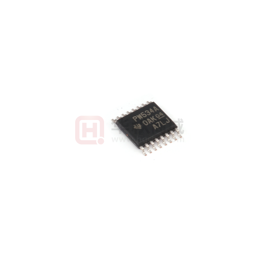


 工商网监
湘ICP备2023018690号
工商网监
湘ICP备2023018690号
