Order
Now
Product
Folder
Support &
Community
Tools &
Software
Technical
Documents
TDP158
SLLSEX2D – DECEMBER 2016 – REVISED MARCH 2020
TDP158 6-Gbps, AC-Coupled to TMDS™ or HDMI™ Level Shifter Redriver
1 Features
3 Description
•
The TDP158 device is an AC-Coupled HDMI signal to
transition-minimized differential signal (TMDS)
Redriver supporting digital video interface (DVI) 1.0
and high-definition multimedia interface (HDMI) 1.4b
and 2.0b output signals. The TDP158 supports four
TMDS channels and Digital Display Control (DDC)
interfaces. The TDP158 supports signaling rates up
to 6 Gbps to allow for the highest resolutions of
4k2k60p 24 bits per pixel and up to WUXGA 16-bit
color depth or 1080p with higher refresh rates. The
TDP158 can be configured to support the HDMI2.0
standard.
1
•
•
•
•
•
•
•
•
•
AC-coupled TMDS or DisplayPort Dual-Mode
Physical Layer Input to HDMI2.0bTMDS Physical
Layer Output Supporting up to 6 Gbps Data Rate,
Compatible with HDMI2.0b Electrical Parameters
Supporting DisplayPort Dual-Mode Standard
Version 1.1
Support 4k2k60p and up to WUXGA 16-bit Color
Depth or 1080p with Higher Refresh Rates
Programmable Fixed Receiver Equalizer up to
15.5 dB
Global or Independent High Speed Lane Control,
Pre-emphasis and Transmit Swing, and Slew Rate
Control
I2C or Pin Strap Programmable
Configurable as a DisplayPort Redriver via I2C
Full Lane Swap on Main Lanes
Low Power Consumption
– –200 mW Active at 6-Gbps and –8 mW at
Shutdown State
40-pin, 0.4 mm Pitch, 5 mm x 5 mm, WQFN
Package, Pin Compatible to the SN75DP159RSB
Retimer
The TDP158 supports dual power supply rails of
1.1 V on VDD and 3.3 V on VCC for power reduction.
Several methods of power management are
implemented to reduce overall power consumption.
TDP158 supports fixed receiver EQ gain using I2C or
pin strap to compensate for different lengths input
cable or board traces.
Device Information(1)
PART NUMBER
PACKAGE
TDP158
WQFN (40)
BODY SIZE (NOM)
5.00 mm x 5.00 mm
(1) For all available packages, see the orderable addendum at
the end of the data sheet.
2 Applications
•
•
•
•
•
•
Notebook, Desktop, All-in-Ones, Tablet, Gaming
and Industrial PC
Audio/Video Equipment
Blu-ray™ DVD
Gaming Systems
HDMI Adaptor or Dongle
Docking Station
Spacer
Simplified Schematic
Display
TDP158
DP++ TX
Or
AC Coupled
HDMI TX
IN_D2p/n
OUT_D2p/n
IN_D1p/n
OUT_D1p/n
IN_D0p/n
IN_CLKp/n
GPU
OUT_D0p/n
OUT_CLKp/n
5V
SCL_SRC
HDMI
Connector
D P1
58
T
TDP158
SDA_SRC
SCL_SNK
DDC
SDA_SNK
HPD
3.3 V
HPD_SRC
HPD_SNK
OE
2
IC
SCL_CTL
VSADJ
SDA_CTL
Copyright © 2016, Texas Instruments Incorporated
1
An IMPORTANT NOTICE at the end of this data sheet addresses availability, warranty, changes, use in safety-critical applications,
intellectual property matters and other important disclaimers. PRODUCTION DATA.
�TDP158
SLLSEX2D – DECEMBER 2016 – REVISED MARCH 2020
www.ti.com
Table of Contents
1
2
3
4
5
6
Features ..................................................................
Applications ...........................................................
Description .............................................................
Revision History.....................................................
Pin Configuration and Functions .........................
Specifications.........................................................
1
1
1
2
4
6
6.1
6.2
6.3
6.4
6.5
6.6
6.7
Absolute Maximum Ratings ...................................... 6
ESD Ratings.............................................................. 6
Recommended Operating Conditions....................... 6
Thermal Information .................................................. 7
Electrical Characteristics, Power Supply ................. 8
Electrical Characteristics, Differential Input ............. 9
Electrical Characteristics, TMDS Differential Output
...................................................................................9
6.8 Electrical Characteristics, DDC, I2C, HPD, and ARC
...................................................................................9
6.9 Electrical Characteristics, TMDS Differential Output in
DP-Mode .................................................................. 10
6.10 Switching Characteristics, TMDS.......................... 11
6.11 Switching Characteristics, HPD ............................ 11
6.12 Switching Characteristics, DDC and I2C .............. 11
6.13 Typical Characteristics .......................................... 12
7
8
Parameter Measurement Information ................ 13
Detailed Description ............................................ 19
8.1
8.2
8.3
8.4
8.5
9
Overview .................................................................
Functional Block Diagram .......................................
Feature Description.................................................
Device Functional Modes........................................
Register Maps .........................................................
19
20
20
27
28
Application and Implementation ........................ 39
9.1 Application Information............................................ 39
9.2 Typical Application ................................................. 39
10 Power Supply Recommendations ..................... 45
10.1 Power Management .............................................. 45
10.2 Standby Power...................................................... 45
11 Layout................................................................... 46
11.1 Layout Guidelines ................................................. 46
11.2 Layout Example .................................................... 47
12 Device and Documentation Support ................. 48
12.1
12.2
12.3
12.4
12.5
12.6
Documentation Support .......................................
Receiving Notification of Documentation Updates
Community Resources..........................................
Trademarks ...........................................................
Electrostatic Discharge Caution ............................
Glossary ................................................................
48
48
48
48
48
48
13 Mechanical, Packaging, and Orderable
Information ........................................................... 49
4 Revision History
Changes from Revision C (October 2019) to Revision D
•
Page
Changed HDMI2.0a to HDMI2.0b .......................................................................................................................................... 1
Changes from Revision B (June 2017) to Revision C
Page
•
Deleted Feature: Both Extended Commercial and Industrial Temperature Device Options .................................................. 1
•
Changed Feature: From: Pin Compatible to the SN65DP159RSB and SN75DP159RSB Retimer To: Pin Compatible
to the SN75DP159RSB Retimer............................................................................................................................................. 1
•
Deleted TDP158I from the Device Information table.............................................................................................................. 1
•
Changed the TJ MIN value From: –40°C To: 0°C in the Recommended Operating Conditions table ................................... 6
•
Deleted TA for TDP158I in the Recommended Operating Conditions table........................................................................... 6
•
Changed the last sentence of the Overview section to remove the TDP158I device .......................................................... 19
Changes from Revision A (January 2017) to Revision B
Page
•
Changed the title From: "HDMI™ Redriver" To: "HDMI™ Level Shifter Redriver" ................................................................ 1
•
Changed the Features List ..................................................................................................................................................... 1
•
Changed the Applications List ................................................................................................................................................ 1
•
Added text to pins 17, 23, 34, 16 in the Pin Functions table: "For pin control, Low = 1 kΩ pulldown resistor to GND,
High = 1 kΩ pullup resistor to VCC, NC = Floating" .............................................................................................................. 5
•
Added text to pin NC in the Pin Functions table: "Optionally connect 0.1 μF to GND to reduce noise" ................................ 5
•
VSADJ: Added Note "Reducing resistor ..", and Changed values in the Recommended Operating Conditions table............. 6
•
Changed Rvsdj max value to 8 kΩ in Figure 1 .................................................................................................................... 12
2
Submit Documentation Feedback
Copyright © 2016–2020, Texas Instruments Incorporated
�TDP158
www.ti.com
SLLSEX2D – DECEMBER 2016 – REVISED MARCH 2020
•
Changed the paragraph in the Operation Timing section .................................................................................................... 21
•
Added column Pin Number to Table 2, Changed IN_CLK → OUT_CLK To: IN_D2 → OUT_D2 in the last row of the
SWAP column....................................................................................................................................................................... 22
•
Changed Note 1 of Table 3 ................................................................................................................................................. 23
•
Changed the last two sentences of the paragraph in the Pre-emphasis section ................................................................. 26
•
Changed the title of Figure 23 From: 3.5 dB Pre-emphasis in Normal Operation To: 6 dB Pre-emphasis Setting in
Normal Operation ................................................................................................................................................................. 26
•
Changed From: Reg0Ch[1:0] = 01 To: Reg0Ch[1:0] = 10 in Figure 24 ............................................................................... 26
•
Changed the Default setting in Table 9 From: TBD To: 00000001...................................................................................... 30
•
Added paragraph to the Application and Implementation section: "TDP158 is designed ..."............................................... 39
•
Changed the Application Information paragraph .................................................................................................................. 39
•
Changed From: 0 Ω resistors To: 1 kΩ resistors, and a noise filter (capacitor) for the no connect in Figure 42................. 39
•
Added text "1 kΩ pulldown resistor " to the Connect values in Table 25 ............................................................................ 40
•
Changed text in the second paragraph of the Source Side HDMI Application section From: "Control pins can be tied
directly to VCC, GND or left floating." To: "Control pins should be tied to 1 kΩ pullup to VCC, 1 kΩ pulldown to
GND, or left floating."............................................................................................................................................................ 43
•
Changed From: 0 Ω resistors To: 1 kΩ resistors, and a noise filter (capacitor) for the no connect in Figure 46................. 43
•
Changed From: 0 Ω resistors To: 1 kΩ resistors, and a noise filter (capacitor) for the no connect in Figure 47................. 44
•
Changed From: 0 Ω resistors To: 1 kΩ resistors, and a noise filter (capacitor) for the no connect in Figure 49................. 47
Changes from Original (December 2016) to Revision A
•
Page
Changed From: Preview To: Production data ....................................................................................................................... 1
Copyright © 2016–2020, Texas Instruments Incorporated
Submit Documentation Feedback
3
�TDP158
SLLSEX2D – DECEMBER 2016 – REVISED MARCH 2020
www.ti.com
5 Pin Configuration and Functions
VDD
SDA_SRC
SCL_SRC
VCC
OE
GND
SLEW
SDA_SNK
SCL_SNK
VDD
40
39
38
37
36
35
34
33
32
31
RSB Package
WQFN (40 Pins)
Top View
IN_D2p/n
1
30
OUT_D2n/p
IN_D2p/n
2
29
OUT_D2n/p
HPD_SRC
3
28
HPD_SNK
IN_D1p/n
4
27
OUT_D1n/p
IN_D1p/n
5
26
OUT_D1n/p
IN_D0p/n
6
25
OUT_D0n/p
IN_D0p/n
7
24
OUT_D0n/p
I2C_EN
8
23
A1/EQ2
IN_CLKp/n
9
22
OUT_CLKn/p
IN_CLKp/n
10
21
OUT_CLKn/p
11
12
13
14
15
16
17
18
19
20
VCC
VDD
SCL_CTL/SWAP
SDA_CTL/PRE
GND
TERM
A0/EQ1
VSADJ
NC
VDD
GND
Not to scale
Pin Functions
PIN
NAME
NO.
I/O
DESCRIPTION
SUPPLY AND GROUND PINS
VCC
11, 37
P
3.3V Power Supply
VDD
12,20,31,40
P
1.1V Power Supply
GND
15, 35
Thermal Pad
G
Ground
MAIN LINK INPUT PINS
IN_D2p/n
1, 2
I
Channel 2 Differential Input
IN_D1p/n
4, 5
I
Channel 1 Differential Input
IN_D0p/n
6, 7
I
Channel 0 Differential Input
IN_CLKp/n
9, 10
I
Clock Differential Input
OUT_D2n/p
29, 30
O
TMDS Data 2 Differential Output
OUT_D1n/p
26, 27
O
TMDS Data 1 Differential Output
OUT_D0n/p
24, 25
O
TMDS Data 0 Differential Output
OUT_CLKn/p
21, 22
O
TMDS Data Clock Differential Output
MAIN LINK OUTPUT PINS (FAIL SAFE)
4
Submit Documentation Feedback
Copyright © 2016–2020, Texas Instruments Incorporated
�TDP158
www.ti.com
SLLSEX2D – DECEMBER 2016 – REVISED MARCH 2020
Pin Functions (continued)
PIN
NAME
NO.
I/O
DESCRIPTION
HOT PLUG DETECT AND DDC PINS
HPD_SRC
3
O
Hot Plug Detect Output to source side
HPD_SNK
28
I
Hot Plug Detect Input from sink side
SDA_SNK
33
I/O
Sink Side Bidirectional DDC Data Line
SCL_SNK
32
I/O
Sink Side Bidirectional DDC Clock Line
SDA_SRC
39
I/O
Source Side Bidirectional DDC Data Line
SCL_SRC
38
I/O
Source Side Bidirectional DDC Clock Line
CONTROL PINS
OE
36
I
Operation Enable/Reset Pin
OE = L: Power Down Mode
OE = H: Normal Operation
Internal weak pullup: Resets device when transitions from H to L
I2C_EN
8
I
I2C_EN = High; Puts Device into I2C Control Mode
I2C_EN = Low; Puts Device into Pin Strap Mode
SDA_CTL/PRE
14
I/0
SCL_CTL/SWAP
13
I
I2C Clock Signal: When I2C_EN = High;
Lane SWAP: When I2C_EN = Low: See Swap HDMI Mode Only
SWAP = L: Normal Operation
SWAP = H: Lane Swap
VSADJ
18
I
TMDS Compliant Voltage Swing Control (Nominal 6 kΩ for HDMI and DP combination;
6.49 kΩ for HDMI only)
17
I
3 Level
Address Bit 1 for I2C Programming when I2C_EN = High
EQ1 Pin Setting when I2C_EN = Low; Works in conjunction with A1/EQ2; See Main Link
Inputs for settings. For pin control, Low = 1 kΩ pulldown resistor to GND, High = 1 kΩ
pullup resistor to VCC, NC = Floating.
23
I
3 Level
Address Bit 2 for I2C Programming when I2C_EN = High
EQ2 Pin Setting when I2C_EN = Low; Works in conjunction with A0/EQ1; See Main Link
Inputs for settings. For pin control, Low = 1 kΩ pulldown resistor to GND, High = 1 kΩ
pullup resistor to VCC, NC = Floating.
I
3 Level
Clock Slew Rate Control: See Slew Rate Control
SLEW = L: Slowest ~ 203 ps
SLEW = NC (Default): Mid-range 1 ~ 180 ps
SLEW = H: Fastest ~ 122 ps
For pin control, L = 1 kΩ pulldown resistor to GND, H = 1 kΩ pullup resistor to VCC, NC
= Floating.
Source Termination Cotnrol: See Transmitter Impedance Control
TERM = H, 75 Ω ~ 150 Ω
TERM = L, Transmit Termination impedance in 150 Ω ~ 300 Ω
TERM = NC, No transmit Termination
Note: When TMDS_CLOCK_RATIO_STATUS bit = 1 the TDP158 sets source
termination to 75 Ω ~ 150 Ω Automatically
For pin control, L = 1 kΩ pulldown resistor to GND, H = 1 kΩ pullup resistor to VCC, NC
= Floating.
A0/EQ1
A1/EQ2
SLEW
34
TERM
16
I
3 Level
NC
19
NA
Copyright © 2016–2020, Texas Instruments Incorporated
I2C Data Signal: When I2C_EN = High;
Pre-emphasis: When I2C_EN = Low: See Pre-emphasis
DE = L: None 0 dB
DE = H: 3.5 dB
No Connect. Optionally connect 0.1 μF to GND to reduce noise.
Submit Documentation Feedback
5
�TDP158
SLLSEX2D – DECEMBER 2016 – REVISED MARCH 2020
www.ti.com
6 Specifications
6.1 Absolute Maximum Ratings
over operating free-air temperature range (unless otherwise noted) (1) (2)
Supply Voltage Range (3)
MIN
MAX
UNIT
VCC
–0.3
4
V
VDD
–0.3
1.4
V
0
1.56
V
Main Link Input Single Ended on Pin
–0.3
1.4
V
TMDS Output ( OUT_Dx)
–0.3
4
V
HPD_SRC, VSADJ, SDA_CTL/PRE, OE,
A1/EQ2, A0/EQ1, TERM, I2C_EN, SLEW,
SCL_CTL/SWAP, SDA_SRC, SCL_SRC
–0.3
4
V
HDP_SNK, SDA_SNK, SCL_SNK
–0.3
6
V
Main Link Input Differential Voltage (IN_Dx)
Voltage Range
Continuous power dissipation
See Thermal Information
Storage temperature, Tstg
(1)
(2)
(3)
–65
150
°C
Stresses beyond those listed under Absolute Maximum Ratings may cause permanent damage to the device. These are stress ratings
only, which do not imply functional operation of the device at these or any other conditions beyond those indicated under Recommended
Operating Conditions. Exposure to absolute-maximum-rated conditions for extended periods may affect device reliability.
All voltage values, except differential voltages, are with respect to network ground terminal.
Tested in accordance with JEDEC Standard 22, Test Method A114-B
6.2 ESD Ratings
VALUE
V(ESD)
(1)
(2)
Electrostatic discharge
Human-body model (HBM), per ANSI/ESDA/JEDEC JS-001 (1)
±2000
Charged-device model (CDM), per JEDEC specification JESD22C101 (2)
±500
UNIT
V
JEDEC document JEP155 states that 500-V HBM allows safe manufacturing with a standard ESD control process.
JEDEC document JEP157 states that 250-V CDM allows safe manufacturing with a standard ESD control process.
6.3 Recommended Operating Conditions
over operating free-air temperature range (unless otherwise noted)
MIN
Supply Voltage Nominal Value 3.3 V for DP mode
VCC
Supply Voltage Nominal Value 3.3 V for HDMI mode
NOM
MAX
UNIT
3
3.6
V
3.13
3.47
V
VDD
Supply Voltage Nominal Value 1.1 V
1
1.27
V
TJ
Junction temperature
0
105
°C
TA
Operating free-air temperature (TDP158)
0
85
°C
MAIN LINK DIFFERENTIAL PINS
VID(EYE)
Peak-to-peak input differential voltage See Figure 17
75
1200
mV
VID(DC)
The input differential voltage Peak-to peak DC level, See Figure 17
200
1200
mV
VIC
Input Common Mode Voltage (Internally Biased)
0.5
0.9
dR
Data rate
0.25
6
Gbps
VSADJ
TMDS compliant swing voltage bias resistor (Nominal 6 kΩ for HDMI and
DP combination; 6.49 kΩ for HDMI only) (1)
4.5
8
kΩ
HDP_SNK, SDA_SNK, SCL_SNK,
–0.3
5.5
V
SDA_SRC, SCL_SRC; All other Local I2C, and
control pins
–0.3
3.6
V
V
DDC, I2C, HPD, AND CONTROL PINS
VI(DC)
(1)
6
DC Input Voltage
Reducing resistor in VSADJ will increase VOD, care should be taking since resistors below ~6 kΩ may lead to compliance failures.
Submit Documentation Feedback
Copyright © 2016–2020, Texas Instruments Incorporated
�TDP158
www.ti.com
SLLSEX2D – DECEMBER 2016 – REVISED MARCH 2020
Recommended Operating Conditions (continued)
over operating free-air temperature range (unless otherwise noted)
MIN
VIL
VIM
MAX
UNIT
Low-level input voltage at DDC
0.3 x VCC
V
Low-level input voltage at HPD
0.8
V
Low-level input voltage at SDA_CTL/PRE, OE, A1/EQ2, A0/EQ1, TERM,
I2C_EN, SLEW, SCL_CTL/SWAP pins only
0.3
V
1.6
V
Mid-Level input voltage at A1/EQ2, A0/EQ1, TERM, SLEW pins only
VIH
NOM
1.2
High-level input voltage at OE, A1/EQ2, A0/EQ1, TERM, I2C_EN, SLEW
pins only
0.7 x VCC
V
High-level input voltage at SDA_SRC, SCL_SRC, SDA_CTL/PRE,
SCL_CTL/SWAP
0.7 x VCC
V
3.2
V
2
V
High-level input voltage at SDA_SNK, SCL_SNK
High-level input voltage at HPD
VOL
Low-level output voltage
VOH
High-level output voltage
0.4
V
fSCL
SCL clock frequency fast I2C mode for local I2C control
400
kHz
C(bus,DDC)
Total capacitive load for each bus line supporting 400 kHz (DDC
terminals)
400
pF
C(bus,I2C)
Total capacitive load for each bus line (local I2C terminals)
100
pF
dR(DDC)
DDC Data rate
400
kbps
IIH
High level input current
–30
30
µA
IIM
Mid level input current
–20
20
µA
IIL
Low level input current
–10
10
µA
IOZ
High impedance outpupt current
10
µA
R(OEPU)
Pull up resistance on OE pin
150
250
KΩ
2.4
V
6.4 Thermal Information
TDP158
THERMAL METRIC (1)
RSB (WQFN)
UNIT
40 PINS
RθJA
Junction-to-ambient thermal resistance
3.7
°C/W
RθJC(top)
Junction-to-case (top) thermal resistance
23.1
°C/W
RθJB
Junction-to-board thermal resistance
9.9
°C/W
ψJT
Junction-to-top characterization parameter
0.3
°C/W
ψJB
Junction-to-board characterization parameter
3.8
°C/W
RθJC(bot)
Junction-to-case (bottom) thermal resistance
3.2
°C/W
(1)
For more information about traditional and new thermal metrics, see the Semiconductor and IC Package Thermal Metrics application
report.
Copyright © 2016–2020, Texas Instruments Incorporated
Submit Documentation Feedback
7
�TDP158
SLLSEX2D – DECEMBER 2016 – REVISED MARCH 2020
www.ti.com
6.5 Electrical Characteristics, Power Supply
over operating free-air temperature range (unless otherwise noted)
PARAMETER
TEST CONDITIONS
MIN
TYP (1)
MAX (2)
UNIT
200
350
mW
330
680
mW
PD1
Device power Dissipation
OE = H, VCC = 3.3 V/3.6 V, VDD = 1.1
V/1.27 V
IN_Dx: VID_PP = 1200 mV, 6 Gbps TMDS
pattern, VI = 3.3 V, I2C_EN = L,
SDA_CTL/PRE = L, EQ1/EQ2 = H
PD2
Device power Dissipation in DPMode
OE = H, VCC = 3.3 V/3.6 V, VDD = 1.1
V/1.27 V
IN_Dx: VID_PP = 400mV, 5.4 Gbps DP
pattern, I2C_EN = H, VOD = 400 mV PRE =
0 dB
Stage 1: Standby Power
OE = H, VCC = 3.3 V/3.6 V, VDD = 1.1
V/1.27 V , HPD = H, No input Signal: Stage
1 See Standby Power
34
mW
Stage 2: Standby Power
OE = H, VCC = 3.3 V/3.6 V, VDD = 1.1
V/1.27 V , HPD = H, Noise on input Signal:
Stage 2 See Standby Power
60
mW
P(SD1)
Device power in PowerDown
OE = L, VCC = 3.3 V/3.6 V, VDD = 1.1
V/1.27 V
8
34
mW
P(SD2)
Device power in PowerDown in
DP-Mode
OE = L, VCC = 3.3 V/3.6 V, VDD = 1.1
V/1.27 V
8
34
mW
VCC Supply current
OE = H, VCC = 3.3 V/3.6 V, VDD = 1.1
V/1.27 V
IN_Dx: VID_PP = 1200 mV, 6 Gbps TMDS
pattern
I2C_EN = L, SDA_CTL/PRE = L, EQ1/EQ2
= H,
8
20
mA
VCC Supply current in DP-Mode
OE = H, VCC = 3.3 V/3.6 V, VDD = 1.1
V/1.27 V
IN_Dx: VID_PP = 400 mV, 5.4 Gbps DP
pattern, I2C_EN = H, VOD = 400 mV PRE =
0 dB
45
110
mA
VDD Supply current
OE = H, VCC = 3.3 V/3.6 V, VDD = 1.1
V/1.27 V
IN_Dx: VID_PP = 1200 mV, 6 Gbps TMDS
pattern
I2C_EN = L, SDA_CTL/PRE = L, EQ1/EQ2
=H
160
220
mA
VDD Supply current DP-Mode
OE = H, VCC = 3.3 V/3.6 V, VDD = 1.1
V/1.27 V
IN_Dx: VID_PP = 400 mV, 5.4 Gbps DP
pattern, I2C_EN = H, VOD = 40mV PRE =
dB
160
220
mA
Stage 1: Standby current See
Standby Power
OE = H, VCC = 3.3V/3.6V,
VDD = 1.1 V/1.27 V , HPD =
H: No signal on IN_CLK
3.3 V Rail
7
mA
1.1 V Rail
7
mA
OE = H, VCC = 3.3 V/3.6 V,
VDD = 1.1 V/1.27 V , HPD =
H: No valid signal on
IN_CLK
3.3 V Rail
7
mA
Stage 2: Standby current See
Standby Power
1.1 V Rail
27
mA
1
7
mA
PowerDown current – HDMI Mode
OE = L, VCC = 3.3 V/3.6 V,
VDD = 1.1 V/1.27 V , or OE
= H, HPD = L
3.3 V Rail
I(SD11)
1.1 V Rail
4
7
mA
I(SD2)
PowerDown current in DP-Mode
OE = L, VCC = 3.3 V/3.6 V,
VDD = 1.1 V/1.27 V
3.3 V Rail
1
7
mA
1.1 V Rail
4
7
mA
P(STBY1)
ICC1
ICC2
IDD1
IDD2
I(STBY1)
(1)
(2)
8
The Typical rating is simulated at 3.3 V VCC and 1.1 V VDD and at 27°C temperature unless otherwise noted
The Maximum rating is simulated at 3.6 V VCC and 1.27 V VDD and at 85°C temperature unless otherwise noted
Submit Documentation Feedback
Copyright © 2016–2020, Texas Instruments Incorporated
�TDP158
www.ti.com
SLLSEX2D – DECEMBER 2016 – REVISED MARCH 2020
6.6 Electrical Characteristics, Differential Input
over operating free-air temperature range (unless otherwise noted)
PARAMETER
DR(RX_DATA)
TMDS data lanes data rate
DR(RX_CLK)
TMDS clock lanes clock rate
tRX_DUTY
Input clock duty circle
R(INT)
Input differential termination
impedance
V(TERM)
Input Common Mode Voltage
(1)
(2)
TEST CONDITIONS
MAX (2)
UNIT
0.25
6
Gbps
25
340
Mhz
MIN
TYP (1)
40%
50%
60%
80
100
120
OE = H
Ω
0.7
V
The Typical rating is simulated at 3.3 V VCC and 1.1 V VDD and at 27°C temperature unless otherwise noted
The Maximum rating is simulated at 3.6 V VCC and 1.27 V VDD and at 85°C temperature unless otherwise noted
6.7 Electrical Characteristics, TMDS Differential Output
over operating free-air temperature range (unless otherwise noted)
PARAMETER
VOD(PP)
Output differential voltage before Preemphasis; See Pre-emphasis
VOD(SS)
Steady state output differential voltage
See Pre-emphasis
IOS
Short circuit current limit
R(TERM)
Source Termination resistance for
HDMI2.0
(1)
(2)
TEST CONDITIONS
MIN
TYP (1)
MAX (2)
UNIT
VSADJ = 6 kΩ; SDA_CTL/PRE = H:
See Figure 7
600
1400
mV
VSADJ = 6 kΩ; SDA_CTL/PRE = H,
See Figure 7
350
720
mV
VSADJ = 5.5 kΩ; SDA_CTL/PRE = L,
See Figure 6
350
1000
mV
50
mA
150
Ω
Main link output shorted to GND
75
The Typical rating is simulated at 3.3 V VCC and 1.1 V VDD and at 27°C temperature unless otherwise noted
The Maximum rating is simulated at 3.6 V VCC and 1.27 V VDD and at 85°C temperature unless otherwise noted
6.8 Electrical Characteristics, DDC, I2C, HPD, and ARC
over operating free-air temperature range (unless otherwise noted)
PARAMETER
TEST CONDITIONS
MIN
TYP (1)
MAX (2)
UNIT
DDC and I2C
VIL
SCL/SDA_CTL, SCL/SDA_SRC low
level input voltage
VIH
SCL/SDA_CTL, input voltage
V
VCC + 0.5
V
SCL/SDA_CTL, SCL/SDA_SRC low
level output voltage
IO = 3 mA and VCC > 2 V
0.4
V
IO = 3 mA and VCC > 2 V
0.2 x VCC
V
VIH
High-level input voltage
HPD_SNK
VIL
Low-level input voltage
HPD_SNK
VOH
High-level output voltage
IOH
VOL
Low-level output voltage
IOL = 500 µA; HPD_SRC,
Failsafe condition leakage current
VOL
0.7 x VCC
0.3 x VCC
HPD
ILKG
IH(HPD)
R(pdHPD)
(1)
(2)
High level input current
HPD input termination to GND
2.1
V
0.8
V
2.4
3.6
V
0
0.4
V
VCC = 0 V; VDD = 0 V;
HPD_SNK = 5 V;
40
μA
Device powered; VIH = 5 V; IH(HPD)
includes R(pdHPD) resistor current
40
μA
Device powered; VIL = 0.8 V; IL(HPD)
includes R(pdHPD) resistor current
30
μA
220
kΩ
= –500 µA; HPD_SRC,
VCC = 0 V
150
190
The Typical rating is simulated at 3.3 V VCC and 1.1 V VDD and at 27°C temperature unless otherwise noted
The Maximum rating is simulated at 3.6 V VCC and 1.27 V VDD and at 85°C temperature unless otherwise noted
Copyright © 2016–2020, Texas Instruments Incorporated
Submit Documentation Feedback
9
�TDP158
SLLSEX2D – DECEMBER 2016 – REVISED MARCH 2020
www.ti.com
6.9 Electrical Characteristics, TMDS Differential Output in DP-Mode
over operating free-air temperature range (unless otherwise noted)
PARAMETER
TEST CONDITIONS
MIN
TYP
MAX (1)
UNIT
V(TX_DIFFPP_LVL0)
Differential peak-to-peak output
voltage level 0
Based on default state of
V0_P0_VOD register
415
V
V(TX_DIFFPP_LVL1)
Differential peak-to-peak output
voltage level 1
Based on default state of
V1_P0_VOD register
660
V
V(TX_DIFFPP_LVL2)
Differential peak-to-peak output
voltage level 2
Based on default state of
V2_P0_VOD register
880
V
ΔVOD(L1L2)
Output peak-to-peak differential
voltage delta
ΔVODn = 20×log(VODL(n+1) /
VODL(n)) measured in compliance
with latest PHY CTS 1.2
V(TX_PRE_RATIO_0)
Pre-emphasis level 0
RBR, HBR and HBR2
V(TX_PRE_RATIO_1)
Pre-emphasis level 1
RBR, HBR and HBR2
2
4.2
dB
V(TX_PRE_RATIO_2)
Pre-emphasis level 2
RBR, HBR and HBR2
5
7.2
dB
Pre-emphasis delta
Measured in compliance with
latest PHY CTS 1.2
2
dB
1.6
dB
ΔVOD(L0L1)
ΔVPRE(L1L0)
ΔVPRE(L2L1)
(1)
10
1
6
dB
1
5
dB
0
dB
Does not support Level 3 Swing or Pre-emphasis
Submit Documentation Feedback
Copyright © 2016–2020, Texas Instruments Incorporated
�TDP158
www.ti.com
SLLSEX2D – DECEMBER 2016 – REVISED MARCH 2020
6.10 Switching Characteristics, TMDS
PARAMETER
dR
Data rate
tT(DATA)
tT(CLOCK)
(1)
(2)
TEST CONDITIONS
Transition time (rise and fall time);
measured at 20% and 80%.
SDA_CTL = L, OE = H, All Data
Rates
Note: Data lane control by I2C only:
See Slew Rate Control
MIN
TYP (1)
250
MAX (2)
UNIT
6000
Mbps
Reg0Ah[1:0] = 11 (default)
60
ps
Reg0Ah[1:0] = 10
80
ps
Reg0Ah[1:0] = 01
95
ps
Reg0Ah[1:0] = 00
110
ps
TERM = H; Reg0Bh[7:6] = 11
122
ps
Reg0Bh[7:6] = 10
150
ps
TERM = L; Reg0Bh[7:6] = 00
180
ps
TERM = NC; Reg0Bh[7:6] = 01
203
ps
The Typical rating is simulated at 3.3 V VCC and 1.1 V VDD and at 27°C temperature unless otherwise noted
The Maximum rating is simulated at 3.6 V VCC and 1.27 V VDD and at 85°C temperature unless otherwise noted
6.11 Switching Characteristics, HPD
over operating free-air temperature range (unless otherwise noted)
PARAMETER
TEST CONDITIONS
tPD(HPD)
Propagation delay from HPD_SNK
see Figure Figure 11; not valid
to HPD_SRC; rising edge and falling
during switching time
edge
tT(HPD)
HPD logical disconnected timeout
(1)
(2)
see Figure 12
MIN
TYP (1)
MAX (2)
40
120
UNIT
ns
2
ms
The Typical rating is simulated at 3.3 V VCC and 1.1 V VDD and at 27°C temperature unless otherwise noted
The Maximum rating is simulated at 3.6 V VCC and 1.27 V VDD and at 85°C temperature unless otherwise noted
6.12 Switching Characteristics, DDC and I2C
over operating free-air temperature range (unless otherwise noted)
PARAMETER
MAX
UNIT
VCC = 3.3 V; See Figure 15
300
ns
Fall time of both SDA and SCL
signals
See Figure 15
300
ns
tHIGH
Pulse duration , SCL high
See Figure 14
tLOW
Pulse duration , SCL low
See Figure 14
1.3
μs
tSU1
Setup time, SDA to SCL
See Figure 14
100
ns
Setup time, SCL to start condition
See Figure 14
0.6
μs
tHD,STA
Hold time, start condition to SCL
See Figure 13
0.6
μs
tHD,DAT
Data Hold Time
0
ns
tVD,DAT
Data valid time
0.9
µs
tVD,ACK
Data valid acknowledge time
0.9
µs
tST,STO
Setup time, SCL to stop condition
See Figure 13
0.6
μs
t(BUF)
Bus free time between stop and start
See Figure 13
condition
1.3
μs
tr
Rise time of both SDA and SCL
signals
tf
tST,
STA
Copyright © 2016–2020, Texas Instruments Incorporated
TEST CONDITIONS
MIN
TYP
0.6
Submit Documentation Feedback
μs
11
�TDP158
SLLSEX2D – DECEMBER 2016 – REVISED MARCH 2020
www.ti.com
900
180
800
160
700
140
600
120
Current (mA)
VOD (mV)
6.13 Typical Characteristics
500
400
300
100
80
60
200
40
100
20
0
1.1 V (mA)
3.3 V (mA)
0
4
5
6
Rvsadj (k:)
7
8
0
0.5
1
1.5
2
D001
Figure 1. VOD Swing vs VASDJ Resistor Value
2.5 3 3.5 4
Date Rate (Gbps)
4.5
5
5.5
6
D002
Figure 2. HDMI Current vs Data Rate
180
160
Current (mA)
140
120
100
80
60
40
20
0
1.4
2
2.6
3.2
3.8
Data Rate (Gbps)
4.4
5
5.4
D003
Figure 3. DisplayPort Current vs Data Rate
12
Submit Documentation Feedback
Copyright © 2016–2020, Texas Instruments Incorporated
�TDP158
www.ti.com
SLLSEX2D – DECEMBER 2016 – REVISED MARCH 2020
7 Parameter Measurement Information
VTERM
3.3 V
50 Ÿ
50 Ÿ
75-200 nF
50 Ÿ
50 Ÿ
D+
VD+
0.5 pF
Receiver
VID
Y
Driver
VY
D75-200 nF
Z
VD-
VID = VD+ - VD-
VOD = VY - VZ
VICM = (VD+ + VD-)
2
VOC = (VY + VZ)
2
VZ
Copyright © 2016, Texas Instruments Incorporated
Figure 4. TMDS Main Link Test Circuit
4.0 V
Vcc
VID
2.6 V
VID+
VID(pp)
0V
VIDtPHL
tPLH
80%
80%
VOD
VOD(pp)
0V
20%
tf
20%
tr
Figure 5. Input or Output Timing Measurements
Copyright © 2016–2020, Texas Instruments Incorporated
Submit Documentation Feedback
13
�TDP158
SLLSEX2D – DECEMBER 2016 – REVISED MARCH 2020
www.ti.com
Parameter Measurement Information (continued)
VOD(SS)
PRE = L
Figure 6. Output Differential Waveform
PRE = L
PRE = H
VOD(PP)
VOD(SS)
Figure 7. Output Differential Waveform with De-empahsis
14
Submit Documentation Feedback
Copyright © 2016–2020, Texas Instruments Incorporated
�TDP158
www.ti.com
SLLSEX2D – DECEMBER 2016 – REVISED MARCH 2020
Parameter Measurement Information (continued)
Avcc(4)
RT
Data +
Parallel (6)
BERT
Data -
Coax
Coax
SMA
RX
+EQ
SMA
FR4 PCB trace(1) &
AC coupling Caps
[No Preemphasis]
Clk+
Clk-
Coax
Coax
Coax
SMA
Coax
Device
Jitter Test
Instrument (2,3)
FR4 PCB trace
AVcc
RT
RX
+EQ
RT(5)
REF
Cable
EQ
OUT
SMA
SMA
SMA
SMA
Coax
SMA
Coax
OUT
RT
REF
Cable
EQ
Jitter Test
Instrument (2,3)
TTP1
TTP2
TTP3
TTP2_EQ
TTP4_EQ
TTP4
Copyright © 2016, Texas Instruments Incorporated
(1)
The FR4 trace between TTP1 and TTP2 is designed to emulate 1-8” of FR4, AC coupling cap, connector and another
1-8” of FR4. Trace width – 4 mils. 100 Ω differential impedance.
(2)
All Jitter is measured at a BER of 109
(3)
Residual jitter reflects the total jitter measured at TTP4 minus the jitter measured at TTP
(4)
AVCC = 3.3 V
(5)
RT = 50 Ω
(6)
The input signal from parallel Bert does not have any pre-emphasis. Refer to Recommended Operating Conditions.
Figure 8. HDMI Output Jitter Measurement
V
0
H
0
0.5
Figure 9. Output Eye Mask at TTP4_EQ for HDMI 2.0
TMDS Data Rate (Gbps)
H (Tbit)
3.4 < DR < 3.712
0.6
335
3.712 < DR < 5.94
–0.0332Rbit2 + 0.2312 Rbit + 0.1998
–19.66Rbit2 + 106.74Rbit + 209.58
5.94 ≤ DR ≤ 6.0
0.4
150
Copyright © 2016–2020, Texas Instruments Incorporated
V (mV)
Submit Documentation Feedback
15
�TDP158
SLLSEX2D – DECEMBER 2016 – REVISED MARCH 2020
www.ti.com
HPD Input
HPD Output
190 K
100K
Figure 10. HPD Test Circuit
VCC
HPD_SNK
50%
0V
tPD(HPD)
VCC
HPD_SRC
50%
0V
Figure 11. HPD Timing Diagram No. 1
Vcc
HPD_SNK
50%
0V
HPD_SRC
HPD Logical disconnect
Timeout
tT(HPD)
Vcc
0V
Device Logically
Connected
Logically
Disconnected
Figure 12. HPD Logic Disconnect Timeout
16
Submit Documentation Feedback
Copyright © 2016–2020, Texas Instruments Incorporated
�TDP158
www.ti.com
SLLSEX2D – DECEMBER 2016 – REVISED MARCH 2020
tHD,STA
tf
tr
SCL
tST,STO
SDA
t(BUF)
START
STOP
Figure 13. Start and Stop Condition Timing
tHIGH
tLOW
SCL
tST,STA
SDA
tSU1
Figure 14. SCL and SDA Timing
Copyright © 2016–2020, Texas Instruments Incorporated
Submit Documentation Feedback
17
�TDP158
SLLSEX2D – DECEMBER 2016 – REVISED MARCH 2020
www.ti.com
SDA_SRC/SCL_SRC
INPUT
½ VCC
tPLH1
tPHL1
SDA_SNK/SCL_SNK
OUTPUT
80%
½ VCC
20
%
tf
tr
Figure 15. DDC Propagation Delay – Source to Sink
SDA_SNK/SCL_SNK
INPUT
½ Vcc
tPHL2
tPLH2
80%
SDA_SRC/SCL_SRC
OUTPUT
20%
tf
½ Vcc
tr
Figure 16. DDC Propagation Delay – Sink to Source
VID(DC)
VID(EYE)
Figure 17. VID(DC) and VID(EYE)
18
Submit Documentation Feedback
Copyright © 2016–2020, Texas Instruments Incorporated
�TDP158
www.ti.com
SLLSEX2D – DECEMBER 2016 – REVISED MARCH 2020
8 Detailed Description
8.1 Overview
The TDP158 is an AC coupled digital video interface (DVI) or high-definition multimedia interface (HDMI) signal
input to Transition Minimized Differential Signal (TMDS) level shifting Redriver. The TDP158 supports four TMDS
channels, Hot Plug Detect, and a Digital Display Control (DDC) interfaces. The TDP158 supports signaling rates
up to 6 Gbps to allow for the highest resolutions of 4k2k60p 24 bits per pixel and up to WUXGA 16-bit color
depth or 1080p with higher refresh rates. For passing compliance and reducing system level design issues
several features have been included such as TMDS output amplitude adjust using an external resistor on the
VSADJ pin, source termination selection, pre-emphasis and output slew rate control. Device operation and
configuration can be programmed by pin strapping or I2C. Four TDP158 devices can be used on one I2C bus
when I2C_EN is high with device address set by A0/A1.
To reduce active power the TDP158 supports dual power supply rails of 1.1 V on VDD and 3.3 V on VCC. There
are several methods of power management such as going into power down mode using three methods:
1. HPD is low
2. Writing a 1 to register 09h[3]
3. de-asserting OE.
De-asserting OE clears the I2C registers, thus once re-asserted, the device must be reprogrammed if I2C was
used for device setup. Upon return to normal active operation from re-asserted, OE or re-asserted HPD, and the
TDP158 requires the source to write a 1 to the TMDS_CLOCK_RATIO_STATUS register in order for the TDP158
to resume 75 Ω to 150 Ω source termination. If during the source to sink read, this bit is already set as a one, the
TDP158 automatically sets this bit to 1. The SIG_EN register enables the signal detect circuit that provides an
automatic power-management feature during normal operation. When no valid signal is present on the clock
input, the device enters Standby mode. DDC link supports the HDMI 2.0b SCDC communication, 100 Kbps data
rate default and 400 kbps adjustable by software.
TDP158 supports fixed EQ gain control to compensate for different lengths of input cables or board traces. The
EQ gain can be software adjusted by I2C control or pin strapping EQ1 and EQ2 pins. Customers can use the
TERM to change to one of three source termination impedances for better output performance when working in
HDMI1.4b or HDMI2.0b. When the TMDS_CLOCK_RATIO_STATUS bit is set to 1, the TDP158 automatically
switches in 75 Ω to 150 Ω source termination. To assist in ease of implementation, the TDP158 supports lanes
swapping, see Lane Control. The device available extended commercial temperature range is 0ºC to 85ºC.
Copyright © 2016–2020, Texas Instruments Incorporated
Submit Documentation Feedback
19
�TDP158
SLLSEX2D – DECEMBER 2016 – REVISED MARCH 2020
www.ti.com
8.2 Functional Block Diagram
HPD_SRC
HPD_SNK
190 .Ÿ
SIGNAL
DETECT
VBIAS
VSADJ
50
Ÿ
OUT_CLKp
TMDS
EQ
TERM
IN_CLKp
50
Ÿ
SIG_DET_
OUT
OUT_CLKn
IN_CLKn
VBIAS
50
Ÿ
OUT_D[2:0]p
EQ
TMDS
IN_D[2:0]n
OUT_D[2:0]n
Enable
I2C_EN
EQ_CTL
EQ1
A0/EQ1
EQ2
A1/EQ2
TERM
IN_D[2:0]p
50
Ÿ
Control Block, I2C Registers
MODE_TERM
SLEW
DE
Enable
SIG_DET_OUT
A0
A1
SDA
SDA_CTL/PRE
SCL
SCL_CTL/SWAP
PRE
OE
Local
I2C
Control
SLEW
TERM
DDC Snoop Block
SWAP
SDA_SRC
SDA_SNK
ACTIVE DDC BLOCK
SCL_SRC
SCL_SNK
1.1 V
VREG 3.3 V
VDD
VCC
GND
Copyright © 2016, Texas Instruments Incorporated
8.3 Feature Description
8.3.1 Reset Implementation
When OE is low, Control signal inputs are ignored; the HDMI inputs and outputs are high impedance. It is critical
to transition the OE from a low level to high after the VCC supply has reached the minimum recommended
operating voltage. This is achieved by a control signal to the OE input, or by an external capacitor connected
between OE and GND. To insure the TDP158 is properly reset, the OE pin must be de-asserted for at least 100
μs before being asserted. When OE is re-asserted the TDP158 must be reprogrammed if it was programmed by
I2C and not pin strapping. When implementing the external capacitor, the size of the external capacitor depends
on the power up ramp of the VCC supply, where a slower ramp-up results in a larger value external capacitor.
Refer to the latest reference schematic for TDP158; consider approximately 0.1 µF capacitor as a reasonable
first estimate for the size of the external capacitor. Both OE implementations are shown in Figure 18 and
Figure 19.
20
Submit Documentation Feedback
Copyright © 2016–2020, Texas Instruments Incorporated
�TDP158
www.ti.com
SLLSEX2D – DECEMBER 2016 – REVISED MARCH 2020
Feature Description (continued)
OE
RRST = 200 KŸ
C
Copyright © 2016, Texas Instruments Incorporated
Figure 18. External Capacitor Controlled OE
GPO
OE
C
Copyright © 2016, Texas Instruments Incorporated
Figure 19. OE Input from Active controller
8.3.2 Operation Timing
TDP158 starts to operate after the OE signal is properly set after power up timing complete. See Figure 20 and
Table 1. Keeping OE low until VDD and VCC become stable avoids any timing requirements as shown in
Figure 20.
Control Signal
Td2
OE
Td1
Vdd
Vcc
Figure 20. Power up Timing for TDP158
Copyright © 2016–2020, Texas Instruments Incorporated
Submit Documentation Feedback
21
�TDP158
SLLSEX2D – DECEMBER 2016 – REVISED MARCH 2020
www.ti.com
Feature Description (continued)
Table 1. Power Up and Operation Timing Requirements
PARAMETER
DESCRIPTION
MIN
0
TYP
MAX
UNIT
200
µs
td1
VCC stable before VDD
td1
VDD and VCC stable before OE de-assertion
100
VDD(ramp)
VDD supply ramp up requirements
0.2
100
ms
VCC(ramp)
VCC supply ramp up requirements
0.2
100
ms
µs
8.3.3 Lane Control
The TDP158 has various lane control features. By default the high speed lanes are globally controlled. Pin
strapping can globally control features like receiver equalization, VOD swing and Pre-emphasis. I2C programming
performs the same global programming using default configurations. Through I2C a method to control receive
equalization, transmitter swing (VOD) and Pre-emphasis on each individual lane. Setting reg09h[5] = 1 puts the
device into independent lane configuration mode.
Reg31h[7:3] controls the clock lane, reg32h[7:3] controls lane D0, reg33h[7:3] controls lane D1 and reg34h[7:3]
controls lane D2 while Reg4E and Reg4F control the individual lane EQ control.
NOTE
If the swap function is enabled and individual lane control has been implemented it is
recommended to reprogram the lanes to make sure they match the expected results.
Register are mapped to the pin name convention.
8.3.4 Swap
TDP158 incorporates a swap function which can swap the lanes, see Figure 21. The EQ, Pre-emphasis,
termination, and slew setup will follow the new mapping. This function can be used with the SCL_CTL/SWAP pin
13 when I2C_EN pin 8 is low or can be implemented using control the register 0x09h bit 7 and is only valid for
HDMI Mode.
Table 2. Swap Functions
22
Normal Operation
SWAP = L or CSR 0x09h bit 7 is 1’b1
Pin Numbers
IN_D2 → OUT_D2
IN_CLK → OUT_CLK
[1, 2] → [30, 29]
IN_D1 → OUT_D1
IN_D0 → OUT_D0
[4, 5] → [27, 26]
IN_D0 → OUT_D0
IN_D1 → OUT_D1
[6, 7] → [25, 24]
IN_CLK → OUT_CLK
IN_D2 → OUT_D2
[9, 10] → [22, 21]
Submit Documentation Feedback
Copyright © 2016–2020, Texas Instruments Incorporated
�TDP158
www.ti.com
DATA LANE2
SLLSEX2D – DECEMBER 2016 – REVISED MARCH 2020
IN_D2p
CLOCK LANE
IN_D2p
1
30
OUT_D2p
2
29
OUT_D2n
IN_D2n
2
29
OUT_D2n
HPD_SRC
3
28
HPD_SNK
HPD_SRC
3
28
HPD_SNK
IN_D1p
4
27
OUT_D1p
IN_D1p
4
27
OUT_D1p
IN_D1n
5
26
OUT_D1n
IN_D0p
6
25
OUT_D0p
DATA LANE0
IN_D1n
DATA LANE0
OUT_D2p
CLOCK LANE
IN_D2n
DATA LANE1
30
1
IN_D0p
5
26
OUT_D1n
6
25
OUT_D0p
DATA LANE1
IN_D0n
7
24
OUT_D0n
IN_D0n
7
24
OUT_D0n
I2C_EN
8
23
A1/EQ2
I2C_EN
8
23
A1/EQ2
IN_CLKp
9
22
OUT_CLKp
IN_CLKp
9
22
OUT_CLKp
IN_CLKn
10
21
OUT_CLKn
DATA LANE2
IN_CLKn
10
21
OUT_CLKn
In Normal Working
Lane Swap
Figure 21. TDP158 Swap Function
8.3.5 Main Link Inputs
Standard Dual Mode DisplayPort terminations are integrated on all inputs with expected AC coupling capacitors
on board prior to input pins. External terminations are not required. Each input data channel contains an
equalizer to compensate for cable or board losses. The voltage at the input pins must be limited under the
absolute maximum ratings.
8.3.6 Receiver Equalizer
The equalizer is used to clean up inter-symbol interference (ISI) jitter/loss from the bandwidth-limited board
traces or cables. TDP158 supports fixed receiver equalizer by setting the A0/EQ1 and A1/EQ2 pins or through
I2C. Table 3 shows the pin strap settings and EQ values.
Table 3. Receiver EQ Programming and Values
Global
RX EQ
(dB)
Pin Control
Independent Lane Control
I2C Control
I2C Control
(2)
{EQ2,EQ1}
P0_Reg0D[6:3]
D2
P0_Reg4E[3:0]
D1
P0_Reg4E[7:4]
D3
P0_Reg4F[3:0]
CLK (2) (3)
P0_Reg4F[7:4]
2
2’b00
4’b0000
4’b0000
4’b0000
4’b0000
4’b0000
3
2’b0Z
4’b0001
4’b0001
4’b0001
4’b0001
4’b0001
4’b0010
4’b0010
4’b0010
4’b0010
4’b0010
4
5
2’b01
4’b0011
4’b0011
4’b0011
4’b0011
4’b0011
6.5
2’bZ0
4’b0100
4’b0100
4’b0100
4’b0100
4’b0100
4’b0101
4’b0101
4’b0101
4’b0101
4’b0101
4’b0110
4’b0110
4’b0110
4’b0110
4’b0110
4’b0111
4’b0111
4’b0111
4’b0111
4’b0111
7.5
8.5
2’bZZ
9
(1)
(2)
(3)
(1)
10
2’bZ1
4’b1000
4’b1000
4’b1000
4’b1000
4’b1000
11
2’b10
4’b1001
4’b1001
4’b1001
4’b1001
4’b1001
For Pin Control 0 = 1 kΩ pulldown resistor to GND, 1 = 1 kΩ pullup resistor to VCC, Z = Floating (No Connect)
Individual Lane control is based upon the pin names with no swap
The CLK EQ in HDMI mode is controlled by register P0_Reg0D[2:1]
Copyright © 2016–2020, Texas Instruments Incorporated
Submit Documentation Feedback
23
�TDP158
SLLSEX2D – DECEMBER 2016 – REVISED MARCH 2020
www.ti.com
Table 3. Receiver EQ Programming and Values (continued)
Global
RX EQ
(dB)
Pin Control
(1)
Independent Lane Control
I2C Control
I2C Control
(2)
P0_Reg0D[6:3]
D2
P0_Reg4E[3:0]
D1
P0_Reg4E[7:4]
D3
P0_Reg4F[3:0]
CLK (2) (3)
P0_Reg4F[7:4]
12
4’b1010
4’b1010
4’b1010
4’b1010
4’b1010
13
4’b1011
4’b1011
4’b1011
4’b1011
4’b1011
14
4’b1100
4’b1100
4’b1100
4’b1100
4’b1100
4’b1101
4’b1101
4’b1101
4’b1101
4’b1101
4’b1110
4’b1110
4’b1110
4’b1110
4’b1110
4’b1111
4’b1111
4’b1111
4’b1111
4’b1111
14.5
{EQ2,EQ1}
2’b1Z
15
15.5
2’b11
8.3.7 Input Signal Detect Block
When SIG_EN is enabled through I2C the receiver looks for a valid HDMI clock signal input and is fully functional
when a valid signal is detected. If no valid HDMI clock signal is detected, the device enters standby mode waiting
for a valid signal at the clock input. All of the TMDS outputs and IN_D[0:2] are in high-Z status. HDMI signal
detect circuit is default enabled. If there is a loss of signal reg20h[5] can be read to determine if the TDP158
hasdetected a valid signal or not.
8.3.8 Transmitter Impedance Control
HDMI2.0 standard requires a source termination impedance in the 75Ω to 150Ω range for data rates > 3.4Gbps.
HDMI1.4b requires no source termination but has a provision for using 150 Ω to 300 Ω for higher data rates. The
TDP158 has three termination levels that are selectable using pin 16 when programming through pin strapping or
when using I2C programming through reg0Bh[4:3]. When the TMDS_CLOCK_RATIO_STATUS bit, reg0Bh[1] = 1
the TDP158 automatically turns on the 75 Ω to 150 Ω source termination otherwise the termination must be
selected. See Table 4.
Table 4. Source Termination Control Table
Pin 16
Reg0Bh[4:3]
Source Termination
TERM = L
00
150 Ω ~ 300 Ω
TERM = NC
01
None
10
Automatic set based upon TMDS_CLOCK_RATIO_STATUS bit
11
75 Ω ~ 150 Ω
TERM = H
NOTE
If the TMDS_CLOCK_RATIO_STATUS bit = 1, the TDP158 automatically switches in 75
Ω ~ 150 Ω termination.
24
Submit Documentation Feedback
Copyright © 2016–2020, Texas Instruments Incorporated
�TDP158
www.ti.com
SLLSEX2D – DECEMBER 2016 – REVISED MARCH 2020
8.3.9 TMDS Outputs
A 1% precision resistor, connected from VSADJ pin to ground is recommended to allow the differential output
swing to comply with TMDS signal levels. The differential output driver provides a typical 10-mA current sink
capability, which provides a typical 500-mV voltage drop across a 50-Ω termination resistor.
VCC
AVCC
TDP158
Zo = RT
Zo = RT
Figure 22. TMDS Driver and Termination Circuit
Referring to Figure 22, if VCC (TDP158 supply) and AVCC (sink termination supply) are both powered, the TMDS
output signals are high impedance when OE = low. Both supplies being active is the normal operating condition.
A total of approximately 33-mW of power is consumed by the terminations independent of the OE logical
selection. When AVCC is powered on, normal operation (OE controls output impedance) is resumed. When the
power source of the device is off and the power source to termination is on, the IO(off), output leakage current,
specification ensures the leakage current is limited 45-μA or less. The clock and data lanes VOD can be changed
through I2C reg0Ch[7:2], VSWING_DATA and VSWING_CLK.
8.3.10 Slew Rate Control
The TDP158 has the ability to slow down the TMDS output edge rates. As the clock signal tends to be a primary
source of EMI the edge rates have been slowed down. There are two ways of changing the slew rate, Pin
strapping for clock lane and I2C for both clock and data lanes. Refer to Switching Characteristics, TMDS
Copyright © 2016–2020, Texas Instruments Incorporated
Submit Documentation Feedback
25
�TDP158
SLLSEX2D – DECEMBER 2016 – REVISED MARCH 2020
www.ti.com
8.3.11 Pre-emphasis
The TDP158 provides Pre-emphasis on the data lanes allowing the output signal pre-conditioning to offset
interconnect losses between the TDP158 outputs and a TMDS receiver. Pre-emphasis is not implemented on the
clock lane unless the TDP158 is in DP Mode and at which time it becomes a data lane. The default value for
Pre-emphasis is 0 dB. There are two methods to implement pre-emphasis, pin strapping or through I2C
programming. When using pin strapping the SDA_CTL/PRE pin controls global pre-emphasis values of 0 dB or
3.5 dB. Through I2C, reg0Ch[1:0] pre-emphasis values are 0 dB, 3.5 dB and 6 dB. The 6 dB value has different
meanings when device is normal operational mode, reg09h[5] = 0, or when the TDP158 has been put into DPMode, reg09h[5] = 1. In normal operation supporting HDMI when selecting 6 dB pre-emphasis the output will be
more on the order of 3 dB pre-emphasis with a 3 dB de-emphasis, see Figure 23. For DP-Mode selecting 6 dB
pre-emphasis the output will be more on the order of 5 dB pre-emphasis with a 1 dB de-emphasis, see
Figure 24. VOD(PP) value will not go above 1 V.
Reg0Ch[1:0] = 00
Reg0Ch[1:0] = 10
VOD(PP)
VOD(SS)
Figure 23. 6 dB Pre-emphasis Setting in Normal Operation
Reg0Ch[1:0] = 00
Reg0Ch[1:0] = 10
VOD(PP)
VOD(SS)
Figure 24. 6 dB Pre-emphasis in DP-Mode
26
Submit Documentation Feedback
Copyright © 2016–2020, Texas Instruments Incorporated
�TDP158
www.ti.com
SLLSEX2D – DECEMBER 2016 – REVISED MARCH 2020
Table 5. Swing and Pre-emphasis Programming Based Upon 6 kΩ VSADJ Resistor
Global Control
Mode
Reg09h[6]
Lane CTL
Reg09[5]
Mode CTL
Independent Lane Control
P0_Reg0C[7:0]
Reg09h[6]
Lane CTL
Reg09[5]
Mode CTL
P0_Reg0C[7:0]
8’h00
HDMI
0
0
8’h00
1
0
DP SWG0, PRE0
0
1
8’h80
1
1
8’h80
DP SWG0, PRE1
0
1
8’hC1
1
1
8’hC1
DP SWG0, PRE2
0
1
8’h42
1
1
8’h42
DP SWG1, PRE0
0
1
8’hC0
1
1
8’hA0
DP SWG1, PRE1
0
1
8’hF1
1
1
8’h21
DP SWG1, PRE2
0
1
8’h52
1
1
8’h62
DP SWG2, PRE0
0
1
8’h20
1
1
8’h00
DP SWG2, PRE1
0
1
8’h51
1
1
8’h61
8.3.12 DP-Mode Description
The TDP158 has the ability to perform as a DisplayPort redriver under the right conditions. The TDP158 is put
into this mode by setting reg09h[5] to 1. The device is now programmable through I2C only. As the transmitter is
a DC coupled transmitter supporting TMDS some external circuits are required to level shift the signal to an AC
coupled DisplayPort signal, see Figure 47. Note that the AUX lines bypass the TDP158. To set the device up
correctly during link training the TDP158 must be programmed using I2C. When this bit is set, the TDP158 does
the following:
• Ignore SWAP function
• Ignore SIG_EN function
• Enable all four lanes and set to support 5.4 Gbps data rate
• Sets VOD swing to the lowest level based on a 6 kΩ VSADJ resistor value
• Sets Pre-emphasis to 0 dB
• Defaults to global lane control
• Can be set to independent lane control by setting P0_Reg09[6] to a 1. This should be done after
implementing DP Mode. Individual Lane control starts on P0_Reg30 through P0_Reg34 and also P0_Reg4E
and 4F
In order for the system implementer to configure the TDP158 output to the properly requested levels during link
training, the following registers are used.
• Reg0Ch[7:5] is a global VOD swing control for all four lanes, see Table 5
• Reg0Ch[1:0] is a global Pre-emphasis control for all four lanes, see Table 5. This register works with
Reg30h[7:6]
• Reg0D[6:3] is a global EQ control for all four lanes
• Reg30h[7:6] is to let the TDP158 know what the data rate is. This is used for the delay component for Preemphasis signal.
• Reg30h[5:2] is used to turn on or off individual lanes
Power down states while in DP-Mode are implemented the same as if in normal operation. See the Electrical
Characteristics, TMDS Differential Output for the outputs based upon the VSADJ 6 kΩ VSADJ resistor.
8.4 Device Functional Modes
8.4.1 DDC Training for HDMI2.0 Data Rate Monitor
As part of discovery the source reads the sink E-EDID information to understand the sink’s capabilities. Part of
this read is HDMI Forum Vendor Specific Data Block (HF-VSDB) MAX_TMDS_Character_Rate byte to determine
the data rate supported. Depending upon the value the source will write to slave address 0xA8 offset 0x20 bit1,
TMDS_CLOCK_RATIO_STATUS. The TDP158 snoops the DDC link to determine the TMDS clock ratio status
and thus sets its own TMDS_CLOCK_RATIO_STATUS bit accordingly. If a ‘1’ is written by the source the TMDS
clock is 1/40 of TMDS bit period. If a ‘0’ is written, then the TMDS clock is 1/10 of TMDS bit period.
Copyright © 2016–2020, Texas Instruments Incorporated
Submit Documentation Feedback
27
�TDP158
SLLSEX2D – DECEMBER 2016 – REVISED MARCH 2020
www.ti.com
Device Functional Modes (continued)
The TDP158 will always default to 1/10 of TMDS bit period unless a ‘1’ is written to address 0xA8 offset 0x20 bit
1 or during a read by the source this bit is set. This helps determine source termination when automatic source
termination select is enabled. Otherwise this bit has no other impact on the TDP158. When HPD_SNK is deasserted this bit is reset to default values of 0 if this feature is enabled. If the source does not write this bit to the
sink or during the read the bit is not set the TDP158 will not set the output termination to 75 Ω to 150 Ω in
support of HDMI2.0. If the TDP158 has entered a power down state using HDP_SNK = low or OE = low this bit is
cleared and will be set on a read or write where this bit is set. When DDC_TRAIN_SETDISABLE is 1’b0 the
TMDS_CLOCK_RATIO_STATUS bit will reflect the value of the DDC snoop. When DDC_TRAIN_SETDISABLE
is 1’b1 the TMDS_CLOCK_RATIO_STATUS bit is set by I2C and DDC snoop is ignored and thus automatic
TERM control is ignored and must be manually set. To go back to snoop and automatic TERM control the
DDC_TRAIN_SETDISABLE bit has to be cleared and TERM set back to automatic control.
8.4.2 DDC Functional Description
The TDP158 solves sink/source level issues by implementing a master/salve control mode for the DDC bus.
When the TDP158 detects the start condition on the DDC bus from the SDA_SRC/SCL_SRC it transfers the data
or clock signal to the SDA_SNK/SCL_SNK with little propagation delay. When SDA_SNK detects the feedback
from the downstream device the TDP158 pulls up or pulls down the SDA_SRC bus and delivers the signal to the
source.
The DDC link defaults to 100kbps but can be set to various values including 400 kbps by setting the correct
value to address 22h through the I2C interface. The HPD goes to high impedance when VCC is under low power
conditions, < 1.5 V.
NOTE
The TDP158 uses clock stretching for DDC transactions. As there are sources and sinks
that do not perform this function correctly a system may not work correctly as DDC
transactions are incorrectly transmitted/received. To overcome this, a snoop configuration
can be implemented where the SDA/SCL from the source is connected directly to the
SDA/SCL pins. The TDP158 needs the SDA_SNK and SCL_SNK pins connected to the
sink DDC pins so that the TMDS_CLOCK_RATIO_STATUS bit can be automatically set
otherwise it will have to be set through I2C. For best noise immunity, the SDA_SRC and
SCL_SRC pins should be connected to GND. Care must be taken when this configuration
is being implemented as the voltage level for DDC between the source and sink may be
different, 3.3 V vs 5 V.
8.5 Register Maps
The TDP158 local I2C interface is enabled when I2C_EN is high. The SCL_CTL and SDA_CTL terminals are
used for I2C clock and data respectively. The TDP158 I2C interface conforms to the two-wire serial interface
defined by the I2C Bus Specification, Version 2.1 (January 2000), and supports the fast mode transfer up to 400
kbps. The device address byte is the first byte received following the START condition from the master device.
The 7 bit device address for TDP158 decides by the combination of A0/EQ1 and A1/EQ2. Table 6 clarifies the
TDP158 target address.
Table 6. TDP158 I2C Device Address Description
A1/A0
Bit 7 (MSB)
Bit 6
Bit 5
Bit 4
Bit 3
Bit 2
Bit 1
Bit 0 (W/R)
HEX
00
1
0
1
1
1
1
0
0/1
BC/BD
01
1
0
1
1
1
0
1
0/1
BA/BB
10
1
0
1
1
1
0
0
0/1
B8/B9
11
1
0
1
1
0
1
1
0/1
B6/B7
The local I2C is 5-V tolerant, and no additional circuitry required. Local I2C buses run at 400 kHz supporting fastmode I2C operation.
28
Submit Documentation Feedback
Copyright © 2016–2020, Texas Instruments Incorporated
�TDP158
www.ti.com
SLLSEX2D – DECEMBER 2016 – REVISED MARCH 2020
The following procedure is followed to write to the TDP158 I2C registers:
1. The master initiates a write operation by generating a start condition (S), followed by the TDP158 7-bit
address and a zero-value “W/R” bit to indicate a write cycle.
2. The TDP158 acknowledges the address cycle.
3. The master presents the sub-address (I2C register within TDP158) to be written, consisting of one byte of
data, MSB-first.
4. The TDP158 acknowledges the sub-address cycle.
5. The master presents the first byte of data to be written to the I2C register.
6. 6. The TDP158 acknowledges the byte transfer.
7. The master may continue presenting additional bytes of data to be written, with each byte transfer completing
with an acknowledge from the TDP158.
8. The master terminates the write operation by generating a stop condition (P).
The following procedure is followed to read the TDP158 I2C registers:
1. The master initiates a read operation by generating a start condition (S), followed by the TDP158 7-bit
address and a one-value “W/R” bit to indicate a read cycle.
2. The TDP158 acknowledges the address cycle.
3. The TDP158 transmit the contents of the memory registers MSB-first starting at register 00h.
4. The TDP158 will wait for either an acknowledge (ACK) or a not-acknowledge (NACK) from the master after
each byte transfer; the I2C master acknowledges reception of each data byte transfer.
5. If an ACK is received, the TDP158 transmits the next byte of data.
6. The master terminates the read operation by generating a stop condition (P).
NOTE
Upon reset, the TDP158 sub-address will always be set to 0x00. When no sub-address is
included in a read operation, the TDP158 sub-address will increment from previous
acknowledged read or write data byte. If it is required to read from a sub-address that is
different from the TDP158 internal sub-address, a write operation with only a sub-address
specified is needed before performing the read operation.
Refer to Local I2C Control BIT Access TAG Convention for TDP158 local I2C register descriptions. Reads from
reserved fields or addresses not specified return zeros. If they are written to and then read they will read back
what was written but will not impact the device features or performance.
8.5.1 Local I2C Control BIT Access TAG Convention
Reads from reserved fields shall return zero, and writes to read-only reserved registers shall be ignored. Writes
to reserved register which are marked with ‘W’ will produce unexpected behavior. All addresses not defined by
this specification shall be considered reserved. Reads from these addresses shall return zero and writes shall be
ignored
8.5.2 BIT Access Tag Conventions
A table of bit descriptions is typically included for each register description that indicates the bit field name, field
description, and the field access tags. The field access tags are described in Table 7.
Table 7. Field Access Tags
Access Tag
Name
DESCRIPTION
R
Read
The field shall be read by software
W
Write
The field shall be written by software
S
Set
C
Clear
U
Update
NA
No Access
The field shall be set by a write of one. Writes of Zero to the field have no effect
The field shall be cleared by a write of one. Writes of Zero to the field have no effect
Hardware may autonomously update this field
Not accessible or not applicable
Copyright © 2016–2020, Texas Instruments Incorporated
Submit Documentation Feedback
29
�TDP158
SLLSEX2D – DECEMBER 2016 – REVISED MARCH 2020
www.ti.com
8.5.3 CSR BIT FIELD DEFINITIONS, DEVICE_ID (address = 00h~07h)
Figure 25. DEVICE_ID
7
6
5
4
3
2
1
0
DEVICE_ID
R
LEGEND: R/W = Read/Write; R = Read only; -n = value after reset
Table 8. DEVICE_ID Field Descriptions
Bit
Field
Type
7:0
Default
Description
These fields return a string of ASCII characters “TDP158”
followed by one space characters
TDP158: Address 0x00 – 0x07 = {- 0x54”T”, 0x44”D”, 0x50”P”,
0x31”1”, 0x35”5”, 0x38”8, 0x20, 0x20
R
8.5.4 CSR BIT FIELD DEFINITIONS, REV_ID (address = 08h )
Figure 26. REV_ID Field Descriptions
7
6
5
4
3
2
1
0
REV_ID
R
LEGEND: R/W = Read/Write; R = Read only; -n = value after reset
Table 9. REV_ID
Bit
Field
Type
Default
Description
7:0
REV_ID
R
00000001
This field identifies the device revision.
00000001 – TDP158 Revision
8.5.5 CSR BIT FIELD DEFINITIONS – MISC CONTROL 09h (address = 09h)
Figure 27. MISC CONTROL 09h Field Descriptions
7
LANE_SWAP
6
Lane Control
5
DP-Mode
4
SIG_EN
3
PD_EN
R/W
R/W
R/W
R/W
R/W
2
HPD_AUTO_P
WRDWN_DISA
BLE
R/W
1
0
I2C_DR_CTL
R/W
R/W
LEGEND: R/W = Read/Write; R = Read only; -n = value after reset
Table 10. MISC CONTROL 09h
Bit
7
6
5
30
Field
Type
Default
Description
LANE_SWAP
R/W
1’b0
This field Swaps the input lanes as per Figure 21 and Swap and
valid when in HDMI Mode only.
0 --- Disable ( default ) No Lane Swap
1 --- Enable: Swaps both Input and Output Lanes
1’b0
See Lane Control
0 – Global (Default)
1 – Independent
Note: In default mode reg0C and reg0D control all lanes. When
set to 1 each lane can be individually controlled for Swing, EQ,
Pre-emphasis.
1’b0
See DP-Mode Description
0 – Normal DP158 Operation (Default)
1 – All lanes behave as data lanes and full control through I2C
only
Lane Control
DP-Mode
Submit Documentation Feedback
R/W
R/W
Copyright © 2016–2020, Texas Instruments Incorporated
�TDP158
www.ti.com
SLLSEX2D – DECEMBER 2016 – REVISED MARCH 2020
Table 10. MISC CONTROL 09h (continued)
Bit
Field
Type
Default
Description
4
SIG_EN
R/W
1’b1
This field enable the clock lane activity detect circuitry. See Input
Signal Detect Block
0 – Disable Clock detector circuit closed and receiver always
works in normal operation.
1 – Enable (default) , Clock detector circuit will make receiver
automatic enter the standby state when no valid data detect.
3
PD_EN
R/W
1’b0
0 – Normal working (default)
1 – Forced Power down by I2C, Lowest Power state
2
HPD_AUTO_PWRDWN_DISABL
R/W
1’b0
0 – Automatically enters power down mode based on HPD_SNK
(default)
1 – Will not automatically enter power down mode
2’b10
I2C data rate supported for configuring device.
00 – 5Kbps
01 – 10Kbps
10 – 100Kbps( Default )
11 – 400Kbps
1:0
I2C_DR_CTL
R/W
8.5.6 CSR BIT FIELD DEFINITIONS – MISC CONTROL 0Ah (address = 0Ah)
Figure 28. MISC CONTROL 0Ah Field Descriptions
7
Reserved
R
6
HPDSNK_GAT
E_EN
R/W
5
4
Reserved
3
2
1
0
SLEW_CTL_DATA
R
R/W
LEGEND: R/W = Read/Write; R = Read only; -n = value after reset
Table 11. MISC CONTROL 0Ah
Bit
Field
Type
Default
Description
7
Reserved
R
1’b0
Reserved
6
HPDSNK_GATE_EN
R/W
1’b0
The field set the HPD_SNK signal pass through to HPD_SRC or
not and HPD_SRC whether held in the de-asserted state.
0 – HPD_SNK passed through to the HPD_SRC (default)
1 – HPD_SNK will not pass through to the HPD_SRC.
Reserved
R
4’b0000
Reserved
2’b11
See Slew Rate Control
00 – Slowest ~ 110
01 – Mid-Range 1 ~ 95
10 – Mid-Range 2 ~ 80 ps
11 – Fastest (Default) ~ 60 ps
Values are typical
5:2
1:0
SLEW_CTL_DATA
Copyright © 2016–2020, Texas Instruments Incorporated
R/W
Submit Documentation Feedback
31
�TDP158
SLLSEX2D – DECEMBER 2016 – REVISED MARCH 2020
www.ti.com
8.5.7 CSR BIT FIELD DEFINITIONS – MISC CONTROL 0Bh (address = 0Bh)
Figure 29. MISC CONTROL 0Bh Field Descriptions
7
6
SLEW_CTL_CLK
5
Reserved
R/W
4
3
R
TERM
2
DDC_DR_SEL
R/W
R/W
1
0
TMDS_CLOCK DDC_TRAIN_S
_RATIO_STAT
ETDISABLE
US
R/W/U
R/W
LEGEND: R/W = Read/Write; R = Read only; -n = value after reset
Table 12. MISC CONTROL 0Bh
Bit
7:6
5
4:3
2
1
0
32
Field
Type
Reset
Description
SLEW_CTL_CLK
R/W
2’b01
See Slew Rate Control
00 – Slowest ~ 215 ps
01 – Mid-Range 1 (Default) ~ 185 ps
10 – Mid-Range 2 ~ 155 ps
11 – Fastest ~ 125 ps
Values are typical
Reserved
R
1’b0
Reserved
TERM
R/W
2’b10
Controls termination for HDMI TX. See Transmitter Impedance
Control
00 – 150 to 300 Ω
01 – No termination
10 – Follows TMDS_CLOCK_RATIO_STATUS bit (default).
When = 1 termination value is 75 to 150 Ω:
When = 0 No termination
11 – 75 to 150 Ω:
Note: When TMDS_CLOCK_RATIO_STATUS bit reg0Bh[1] = 1
this register will automatically be set to 11 for 75 to 150 Ω but
can be overwritten using this address
DDC_DR_SEL
R/W
1’b0
Defines the DDC output speed for DDC bridge
0 – 100kbps (default)
1 – 400kbps
1’b0
This field is updated from snoop of I2C write to slave address
0xA8 offset 0x20 bit 1 that occurred on the
SDA_SRC/SCL_SRC interface. When bit 1 of address 0xA8
offset 0x20 is written to a 1’b1 or read as a 1’b1, then this field
will be set to a 1’b1. When bit 1 of address 0xA8 offset 0x20 is
written to a 1’b0, then this field will be set to a 1’b0. This field is
reset to default value whenever HPD_SNK is de-asserted for
greater than 2ms. The main function of this bit is to automatically
set the proper TX termination when value = 1.
0 – HDMI1.4b (default)
1 – HDMI2.0
Note 1. When DDC_TRAIN_SETDISABLE is 1’b0 this bit will
reflect the value of the DDC snoop.
Note 2. When DDC_TRAIN_SETDISABLE is 1’b1 this bit is set
by I2C and DDC snoop is ignored. If this bit was set to 1 during
snoop prior to the DDC_TRAIN_SETDISABLE being set to 1 it
will be cleared to 0.
1’b0
This field indicate the DDC training block function status.
0 – DDC training enable (default)
1 – DDC training disable –DDC snoop disabled
Note 1. When DDC_TRAIN_SETDISABLE is 1’b0 the
TMDS_CLOCK_RATIO_STUATU bit will reflect the value of the
DDC snoop.
Note 2. When DDC_TRAIN_SETDISABLE is 1’b1 this bit is set
by I2C and DDC snoop is ignored and thus automatic TERM
control is ignored and must be manually set and
TMDS_CLOCK_RATIO_STATUS bit will be cleared.
Note 3. To go back to snoop and automatic TERM control this
bit has to be cleared and TERM set back to automatic control.
TMDS_CLOCK_RATIO_STATUS
DDC_TRAIN_SETDISABLE
Submit Documentation Feedback
R/W/U
R/W
Copyright © 2016–2020, Texas Instruments Incorporated
�TDP158
www.ti.com
SLLSEX2D – DECEMBER 2016 – REVISED MARCH 2020
8.5.8 CSR BIT FIELD DEFINITIONS – MISC CONTROL 0Ch (address = 0Ch)
Figure 30. MISC CONTROL 0Ch Field Descriptions
7
6
VSWING_DATA
R/W
5
4
3
VSWING_CLK
R/W
2
1
0
HDMI_TWPST1[1:0]
R/W
LEGEND: R/W = Read/Write; R = Read only; -n = value after reset
Table 13. MISC CONTROL 0Ch
Bit
Field
7:5
Type
VSWING_DATA
4:2
R/W
VSWING_CLK
1:0
R/W
HDMI_TWPST1[1:0]
R/W
Reset
Description
3’b000
Data Output Swing Control
000 – Vsadj set (default)
001 – Increase by 7%
010 – Increase by 14%
011 – Increase by 21%
100 – Decrease by 30%
101 – Decrease by 21%
110 – Decrease by 14%
111 – Decrease by 7%
3’b000
Clock Output Swing Control: Default is set by Vsadj resistor
value and the value of reg0Dh[0].
000 – Vsadj set (default)
001 – Increase by 7%
010 – Increase by 14% 011 – Increase by 21%
100 – Decrease by 30%
101 – Decrease by 21%
110 – Decrease by 14%
111 – Decrease by 7%
2’b00
HDMI Pre-emphasis
00 – No Pre-emphasis (default)
01 – 3.5 dB 10 – 6 dB
11 – Reserved
NOTE: See Pre-emphasis Section for 6 dB explanation during
normal operation supporting HDMI.
8.5.9 CSR BIT FIELD DIFINITIONS, Equalization Control Register (address = 0Dh)
Figure 31. Equalization Control Register
7
Reserved
6
5
4
Data Lane Fixed EQ Values
R
3
2
1
Clock EQ Values
R/W
0
DIS_HDMI2_S
WG
R/W
LEGEND: R/W = Read/Write; R = Read only; -n = value after reset
Table 14. Equalization Control Register Field Descriptions
Bit
Field
Type
Reset
Description
Reserved
R
1’b0
Reserved
6:3
Data Lane Fixed EQ Values
R/W
4’b0000
(Section Receiver Equalizer and Table 3 for values)
0000 – 0 dB (default)
2:1
Clock EQ Values
R/W
2’b00
00 –
01 –
10 –
11 –
1’b0
Disables halving the clock output swing when entering HDMI2.0
mode from TMDS_CLOCK_RATIO_STATUS.
0 – Disables TMDS_CLOCK_RATIO_STATUS control of the
clock VOD so output swing is at full swing (default)
1 – Clock VOD is half of set values when
TMDS_CLOCK_RATIO_STATUS states in HDMI2.0 mode
7
0
DIS_HDMI2_SWG
Copyright © 2016–2020, Texas Instruments Incorporated
R/W
0dB (default)
1.5dB
3dB
4.5dB
Submit Documentation Feedback
33
�TDP158
SLLSEX2D – DECEMBER 2016 – REVISED MARCH 2020
www.ti.com
8.5.10 CSR BIT FIELD DEFINITIONS, POWER MODE STATUS (address = 20h)
Figure 32. POWER MODE STATUS
7
Power Down
Status Bit
6
Standby Status
Bit
R/U
R/U
5
Loss of Signal
Status Bit –
LOS
R/U
4
3
2
Reserved
1
0
R
LEGEND: R/W = Read/Write; R = Read only; -n = value after reset
Table 15. POWER MODE STATUS Field Descriptions
Bit
Field
Type
Reset
Description
7
Power Down Status Bit
R/U
1’b0
0 – Normal Operation
1 – Device in Power Down Mode.
6
Standby Status Bit
R/U
1’b0
0 – Normal Operation
1 – Device in Standby Mode
5
Loss of Signal Status Bit – LOS
R/U
1’b0
0 – Clock present
1 – No Clock present
Reserved
R
5’b00000
Reserved
4:0
8.5.11 CSR BIT FIELD DIFINITIONS, DP-Mode and INDIVIDUAL LANE CONTROL (address = 30h)
See Section 8.3.10 and 8.3.3 Note: DP-Mode is valid only when DP-Mode Register P0_Reg09[5] is set to one
Figure 33. DP-Mode and INDIVIDUAL LANE CONTROL
7
6
Data Rate Select
R/W
R/W
5
Clock Lane
R/W
4
Lane D0
R/W
3
Lane D1
R/W
2
Lane D2
R/W
1
0
Reserved
R
LEGEND: R/W = Read/Write; R = Read only; -n = value after reset
Table 16. DP-Mode and INDIVIDUAL LANE CONTROL Field Descriptions
34
Bit
Field
Type
Reset
Description
7:6
Data Rate Select
R/W
2’b00
00 – 5.4 Gbps (default)
01 – 2.7 Gbps
10 – 1.62 Gbps
11 - Reserved
5
Clock Lane
R/W
1’b1
0 – Disabled
1 – Enabled (default)
4
Lane D0
R/W
1’b1
0 – Disabled
1 – Enabled (default)
3
Lane D1
R/W
1’b1
0 – Disabled
1 – Enabled (default)
2
Lane D2
R/W
1’b1
0 – Disabled
1 – Enabled (default)
1:0
Reserved
R
2’b00
Reserved
Submit Documentation Feedback
Copyright © 2016–2020, Texas Instruments Incorporated
�TDP158
www.ti.com
SLLSEX2D – DECEMBER 2016 – REVISED MARCH 2020
8.5.12 CSR BIT FIELD DIFINITIONS, DP-Mode and INDIVIDUAL LANE CONTROL (address = 31h)
See Section DP-Mode Description and Lane Control Note: DP-Mode is valid only when DP-Mode Register
P0_Reg09[5] is set to one
Figure 34. DP-Mode and INDIVIDUAL LANE CONTROL
7
6
5
VOD Swing Adjust for CLK Lane
4
3
Pre-emphasis Adjust for CLK
Lane
R/W
R/W
2
1
Reserved
0
R/W
LEGEND: R/W = Read/Write; R = Read only; -n = value after reset
Table 17. DP-Mode and INDIVIDUAL LANE CONTROL Field Descriptions
Bit
Field
7:5
Type
VOD Swing Adjust for CLK Lane
R/W
Reset
Description
3’b000
000 – Vsadj set (default)
001 – Increase by 7%
010 – Increase by 14%
011 – Increase by 21%
100 – Decrease by 30%
101 – Decrease by 21%
110 – Decrease by 14%
111 – Decrease by 7%
Note: reg09h[6] = 1 otherwise all lanes are global control.
4:3
Pre-emphasis Adjust for CLK Lane
R/W
2’b00
00 – No Pre-emphasis (default)
01 – 3.5 dB Pre-emphasis.
10 – 6 dB Pre-emphasis
11 – Reserved
Note 1. reg09h[6] = 1 otherwise all lanes are global control.
Note 2. If in HDMI mode writes will be ignored and reg09h[7]
SWAP = 0. No pre-emphasis on clock.
2:0
Reserved
R/W
3’b000
Reserved
8.5.13 CSR BIT FIELD DIFINITIONS, DP-Mode and INDIVIDUAL LANE CONTROL (address = 32h)
See Section DP-Mode Description and Lane Control Note: DP-Mode is valid only when DP-Mode Register
P0_Reg09[5] is set to one
Figure 35. DP-Mode and INDIVIDUAL LANE CONTROL
7
6
5
VOD Swing Adjust for D0 Lane
R/W
4
3
Pre-emphasis Adjust for D0 Lane
R/W
2
1
Reserved
R/W
0
LEGEND: R/W = Read/Write; R = Read only; -n = value after reset
Table 18. DP-Mode and INDIVIDUAL LANE CONTROL Field Descriptions
Bit
7:5
Field
VOD Swing Adjust for D0 Lane
Type
R/W
Reset
Description
3’b000
000 – Vsadj set (default)
001 – Increase by 7%
010 – Increase by 14%
011 – Increase by 21%
100 – Decrease by 30%
101 – Decrease by 21%
110 – Decrease by 14%
11 – Decrease by 7%
Note: reg09h[6] = 1 otherwise all lanes are global control.
4:3
Pre-emphasis Adjust for D0 Lane
R/W
2’b00
00 – No Pre-emphasis (default)
01 – 3.5 dB Pre-emphasis.
10 – 6 dB Pre-emphasis
11 – Reserved
Note: reg09h[6] = 1 otherwise all lanes are global control.
2:0
Reserved
R/W
3’b000
Reserved
Copyright © 2016–2020, Texas Instruments Incorporated
Submit Documentation Feedback
35
�TDP158
SLLSEX2D – DECEMBER 2016 – REVISED MARCH 2020
www.ti.com
8.5.14 CSR BIT FIELD DIFINITIONS, DP-Mode and INDIVIDUAL LANE CONTROL (address = 33h)
See Section DP-Mode Description and Lane Control Note: DP-Mode is valid only when DP-Mode Register
P0_Reg09[5] is set to one
Figure 36. DP-Mode and INDIVIDUAL LANE CONTROL
7
6
5
VOD Swing Adjust for D1 Lane
R/W
4
3
Pre-emphasis Adjust for D1 Lane
R/W
2
1
Reserved
R/W
0
LEGEND: R/W = Read/Write; R = Read only; -n = value after reset
Table 19. DP-Mode and INDIVIDUAL LANE CONTROL Field Descriptions
Bit
Field
7:5
Type
VOD Swing Adjust for D1 Lane
R/W
Reset
Description
3’b000
000 – Vsadj set (default)
001 – Increase by 7%
010 – Increase by 14%
011 – Increase by 21%
100 – Decrease by 30%
101 – Decrease by 21%
110 – Decrease by 14%
11 – Decrease by 7%
Note: reg09h[6] = 1 otherwise all lanes are global control.
4:3
Pre-emphasis Adjust for D1 Lane
R/W
2’b00
00 – No Pre-emphasis (default)
01 – 3.5 dB Pre-emphasis.
10 – 6 dB Pre-emphasis
11 – Reserved
Note: reg09h[6] = 1 otherwise all lanes are global control.
2:0
Reserved
R/W
3’b000
Reserved
8.5.15 CSR BIT FIELD DIFINITIONS, DP-Mode and INDIVIDUAL LANE CONTROL (address = 34h)
See Section DP-Mode Description and Lane Control Note: DP-Mode is valid only when DP-Mode Register
P0_Reg09[5] is set to one
Figure 37. DP-Mode and INDIVIDUAL LANE CONTROL
7
6
5
VOD Swing Adjust for D2 Lane
R/W
4
3
Pre-emphasis Adjust for D2 Lane
R/W
2
1
Reserved
R/W
0
LEGEND: R/W = Read/Write; R = Read only; -n = value after reset
Table 20. DP-Mode and INDIVIDUAL LANE CONTROL Field Descriptions
Bit
7:5
36
Field
VOD Swing Adjust for D2 Lane
Type
R/W
Reset
Description
3’b000
000 – Vsadj set (default)
001 – Increase by 7%
010 – Increase by 14%
011 – Increase by 21%
100 – Decrease by 30%
101 – Decrease by 21%
110 – Decrease by 14%
11 – Decrease by 7%
Note: reg09h[6] = 1 otherwise all lanes are global control.
4:3
Pre-emphasis Adjust for D2 Lane
R/W
2’b00
00 – No Pre-emphasis (default)
01 – 3.5 dB Pre-emphasis.
10 – 6 dB Pre-emphasis
11 – Reserved
Note 1. reg09h[6] = 1 otherwise all lanes are global control.
Note 2. If in HDMI mode writes will be ignored and reg09h[7]
SWAP = 1. No pre-emphasis on clock.
2:0
Reserved
R/W
3’b000
Reserved
Submit Documentation Feedback
Copyright © 2016–2020, Texas Instruments Incorporated
�TDP158
www.ti.com
SLLSEX2D – DECEMBER 2016 – REVISED MARCH 2020
8.5.16 CSR BIT FIELD DIFINITIONS, DP-Mode and INDIVIDUAL LANE CONTROL (address = 35h)
See Section DP-Mode Description and Lane Control Note: DP-Mode is valid only when DP-Mode Register
P0_Reg09[5] is set to one
Figure 38. DP-Mode and INDIVIDUAL LANE CONTROL
7
6
5
4
3
2
1
0
Reserved
R
LEGEND: R/W = Read/Write; R = Read only; -n = value after reset
Table 21. DP-Mode and INDIVIDUAL LANE CONTROL Field Descriptions
Bit
Field
Type
Reset
Description
7:0
Reserved
R
‘h00
Reserved
8.5.17 CSR BIT FIELD DIFINITIONS, DP-Mode and INDIVIDUAL LANE CONTROL (address = 4Dh)
See Section DP-Mode Description and Lane Control Note: DP-Mode is valid only when DP-Mode Register
P0_Reg09[5] is set to one
Figure 39. DP-Mode and INDIVIDUAL LANE CONTROL
7
6
5
4
3
2
1
0
Reserved
R
LEGEND: R/W = Read/Write; R = Read only; -n = value after reset
Table 22. DP-Mode and INDIVIDUAL LANE CONTROL Field Descriptions
Bit
Field
Type
Reset
Description
7:0
Reserved
R
‘h00
Reserved
8.5.18 CSR BIT FIELD DIFINITIONS, DP-Mode and INDIVIDUAL LANE CONTROL (address = 4Eh)
See Section DP-Mode Description and Lane Control Note: DP-Mode is valid only when DP-Mode Register
P0_Reg09[5] is set to one
Figure 40. DP-Mode and INDIVIDUAL LANE CONTROL
7
6
5
Data Lane 1 Fixed EQ Values
R/W
4
3
2
1
Data Lane 2 Fixed EQ Values
R/W
0
LEGEND: R/W = Read/Write; R = Read only; -n = value after reset
Table 23. DP-Mode and INDIVIDUAL LANE CONTROL Field Descriptions
Bit
Field
Type
Reset
Description
7:4
Data Lane 1 Fixed EQ Values
R/W
4’b0000
Section 8.3.6 and Table 8 2 for values
0000 – 0 dB (default)
3:0
Data Lane 2 Fixed EQ Values
R/W
4’b0000
Section 8.3.6 and Table 8 2 for values
0000 – 0 dB (default)
Copyright © 2016–2020, Texas Instruments Incorporated
Submit Documentation Feedback
37
�TDP158
SLLSEX2D – DECEMBER 2016 – REVISED MARCH 2020
www.ti.com
8.5.19 CSR BIT FIELD DIFINITIONS, DP-Mode and INDIVIDUAL LANE CONTROL (address = 4Fh)
See Section DP-Mode Description and Lane Control Note: DP-Mode is valid only when DP-Mode Register
P0_Reg09[5] is set to one
Figure 41. DP-Mode and INDIVIDUAL LANE CONTROL
7
6
5
CLK Lane Fixed EQ Values
R/W
4
3
2
1
Data Lane 0 Fixed EQ Values
R/W
0
LEGEND: R/W = Read/Write; R = Read only; -n = value after reset
Table 24. DP-Mode and INDIVIDUAL LANE CONTROL Field Descriptions
38
Bit
Field
Type
Reset
Description
7:4
CLK Lane Fixed EQ Values
R/W
4’b0000
Section 8.3.6 and Table 8 2 for values
0000 – 0 dB (default)
3:0
Data Lane 0 Fixed EQ Values
R/W
4’b0000
Section 8.3.6 and Table 8 2 for values
0000 – 0 dB (default)
Submit Documentation Feedback
Copyright © 2016–2020, Texas Instruments Incorporated
�TDP158
www.ti.com
SLLSEX2D – DECEMBER 2016 – REVISED MARCH 2020
9 Application and Implementation
NOTE
Information in the following applications sections is not part of the TI component
specification, and TI does not warrant its accuracy or completeness. TI’s customers are
responsible for determining suitability of components for their purposes. Customers should
validate and test their design implementation to confirm system functionality.
TDP158 is designed to accept AC coupled HDMI input signals. The device provides signal conditioning and level
shifting functions to drive a compliant HDMI source connector. The device is not recommended for a HDMI sink
application such as monitor, TV where HDMI compliance is required. TDP158 can be used as an DP/HDMI
redriver in an embedded application where appropriate termination can be ensured. In many major PC or gaming
systems APU/GPU can provide AC coupled HDMI 2.0 signals. TDP158 is suitable for such platforms.
9.1 Application Information
The TDP158 was defined to work in mainly in source applications such as Blu-Ray DVD player, gaming system,
desktop, notebook or AVR. The following sections provide design consideration for various types of applications.
9.2 Typical Application
Figure 42 provides a schematic representation of what is considered a standard implementation.
HDMI/DVI
Receptacle
ML0p
ML0n
ML1p
ML1n
ML2p
ML2n
ML3p
ML3n
0.1uF
1
0.1uF
2
0.1uF
4
0.1uF
5
0.1uF
6
0.1uF
7
0.1uF
9
0.1uF
10
3
HPD
IN_D2p
OUT_D2p
IN_D2n
OUT_D2n
IN_D1p
OUT_D1p
IN_D1n
OUT_D1n
IN_D0p
OUT_D0p
IN_D0n
OUT_D0n
IN_CLKp
OUT_CLKp
IN_CLKn
OUT_CLKn
30
1
29
3
27
4
26
6
25
7
24
9
22
10
21
12
5V
HPD_SRC
2
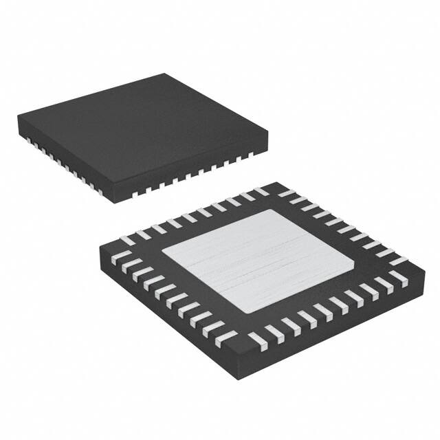


 工商网监
湘ICP备2023018690号
工商网监
湘ICP备2023018690号
