Sample &
Buy
Product
Folder
Support &
Community
Tools &
Software
Technical
Documents
THS4509-Q1
SLOS547A – NOVEMBER 2008 – REVISED NOVEMBER 2015
THS4509-Q1 Wideband Low-Noise Low-Distortion Fully Differential Amplifier
1 Features
3 Description
•
•
•
•
•
•
•
•
•
•
•
•
•
•
•
The THS4509-Q1 is a wideband, fully differential
operational amplifier designed for 5-V dataacquisition systems. It has very low noise at
1.9 nV/√Hz, and extremely low harmonic distortion of
–75-dBc HD2 and –80-dBc HD3 at 100 MHz with
2 Vpp, G = 10 dB, and 1-kΩ load. Slew rate is very
high at 6600 V/μs and with settling time of 2 ns to 1%
(2-V step), it is ideal for pulsed applications. It is
designed for minimum gain of 6 dB but is optimized
for gain of 10 dB.
1
•
Qualified for Automotive Applications
Fully Differential Architecture
Centered Input Common-Mode Range
Minimum Gain of 2 V/V (6 dB)
Bandwidth: 1900 MHz
Slew Rate: 6600 V/μs
1% Settling Time: 2 ns
HD2: –75 dBc at 100 MHz
HD3: –80 dBc at 100 MHz
OIP2: 73 dBm at 70 MHz
OIP3: 37 dBm at 70 MHz
Input Voltage Noise: 1.9 nV/√Hz (f > 10 MHz)
Noise Figure: 17.1 dB
Output Common-Mode Control
Power Supply:
– Voltage: 3 V (±1.5 V) to 5 V (±2.5 V)
– Current: 37.7 mA
Power-Down Capability: 0.65 mA
To allow for dc coupling to analog-to-digital
converters (ADCs), its unique output common-mode
control circuit maintains the output common-mode
voltage within 3-mV offset (typical) from the set
voltage, when set within 0.5 V of mid-supply, with
less than 4-mV differential offset voltage. The
common-mode set point is set to mid-supply by
internal circuitry, which may be overdriven from an
external source.
2 Applications
•
•
•
•
•
•
Adaptive Cruise Control
Blind Spot Detection
Collision Warning
Industrial
5-V Data Acquisition Systems High Linearity ADC
Amplifier
Test and Measurement
The input and output are optimized for best
performance with their common-mode voltages set to
mid-supply. Along with high-performance at low
power-supply voltage, this makes for extremely highperformance single-supply 5-V data-acquisition
systems.
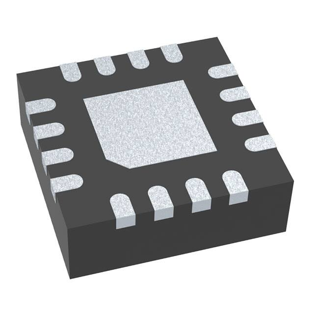
The THS4509-Q1 is offered in a quad 16-pin leadless
QFN package (RGT) and is characterized for
operation over the full automotive temperature range
from –40°C to 125°C.
Device Information(1)
PART NUMBER
THS4509-Q1
MINIMUM GAIN
6 dB
COMMON-MODE
RANGE OF INPUT
0.75 V to 4.25 V
(1) For all available packages, see the orderable addendum at
the end of the data sheet.
Simplified Schematic
From
50 Ω
Source
VIN
100 Ω
2.5 V
69.8 Ω
100 Ω
0.22 µF
49.9 Ω
348 Ω
69.8 Ω
487 Ω
THS 4509
CM
487 Ω
1:1
56.3 Ω
VOUT
To 50 Ω
Test
Equipment
Open
−2.5 V
348 Ω
1
An IMPORTANT NOTICE at the end of this data sheet addresses availability, warranty, changes, use in safety-critical applications,
intellectual property matters and other important disclaimers. PRODUCTION DATA.
�THS4509-Q1
SLOS547A – NOVEMBER 2008 – REVISED NOVEMBER 2015
www.ti.com
Table of Contents
1
2
3
4
5
6
7
Features ..................................................................
Applications ...........................................................
Description .............................................................
Revision History.....................................................
Pin Configuration and Functions .........................
Specifications.........................................................
1
1
1
2
3
4
6.1
6.2
6.3
6.4
6.5
6.6
6.7
4
4
4
4
5
7
9
Absolute Maximum Ratings ......................................
ESD Ratings..............................................................
Recommended Operating Conditions.......................
Thermal Information ..................................................
Electrical Characteristics: VS+ – VS– = 5 V ...............
Electrical Characteristics: VS+ – VS– = 3 V ...............
Typical Characteristics ..............................................
Detailed Description ............................................ 25
7.1 Overview ................................................................. 25
7.2 Functional Block Diagram ....................................... 25
7.3 Feature Description................................................. 25
7.4 Device Functional Modes........................................ 26
8
Application and Implementation ........................ 27
8.1 Application Information............................................ 27
8.2 Typical Applications ................................................ 33
9 Power Supply Recommendations...................... 35
10 Layout................................................................... 36
10.1 Layout Guidelines ................................................. 36
10.2 Layout Example .................................................... 39
11 Device and Documentation Support ................. 40
11.1
11.2
11.3
11.4
11.5
Documentation Support ........................................
Community Resources..........................................
Trademarks ...........................................................
Electrostatic Discharge Caution ............................
Glossary ................................................................
40
40
40
40
40
12 Mechanical, Packaging, and Orderable
Information ........................................................... 40
4 Revision History
NOTE: Page numbers for previous revisions may differ from page numbers in the current version.
Changes from Original (November 2008) to Revision A
•
2
Page
Added ESD Ratings table, Feature Description section, Device Functional Modes, Application and Implementation
section, Power Supply Recommendations section, Layout section, Device and Documentation Support section, and
Mechanical, Packaging, and Orderable Information section ................................................................................................. 1
Submit Documentation Feedback
Copyright © 2008–2015, Texas Instruments Incorporated
Product Folder Links: THS4509-Q1
�THS4509-Q1
www.ti.com
SLOS547A – NOVEMBER 2008 – REVISED NOVEMBER 2015
5 Pin Configuration and Functions
RGT Package
16-Pin QFN
Top View
VS–
16
15
14
13
NC
1
12
PD
VIN–
2
11
VIN+
VOUT+
3
10
VOUT–
CM
4
9
5
6
7
CM
8
VS+
Pin Functions
PIN
I/O
DESCRIPTION
NAME
NO.
CM
4,9
I
NC
1
—
PD
12
I
Power down, PD = logic low puts part into low-power mode, PD = logic high or
open for normal operation
VIN–
2
I
Inverting amplifier input
VIN+
11
I
Noninverting amplifier input
VOUT–
10
O
Inverted amplifier output
VOUT+
3
O
Noninverted amplifier output
VS–
13, 14,
15, 16
I
Negative amplifier power supply input
VS+
5, 6,
7, 8
I
Positive amplifier power-supply input
Common-mode voltage input
No internal connection
Submit Documentation Feedback
Copyright © 2008–2015, Texas Instruments Incorporated
Product Folder Links: THS4509-Q1
3
�THS4509-Q1
SLOS547A – NOVEMBER 2008 – REVISED NOVEMBER 2015
www.ti.com
6 Specifications
6.1 Absolute Maximum Ratings
over operating free-air temperature range (unless otherwise noted) (1)
MIN
VS– to VS+
Supply voltage
VI
Input voltage
VID
Differential input voltage
IO
Output current (2)
–VS
Continuous power dissipation
MAX
UNIT
6
V
+VS
4
V
200
mA
See Thermal Information
TJ
Maximum junction temperature
150
°C
TA
Operating free-air temperature
–40
125
°C
Tstg
Storage temperature
–65
150
°C
(1)
(2)
Stresses beyond those listed under Absolute Maximum Ratings may cause permanent damage to the device. These are stress ratings
only, which do not imply functional operation of the device at these or any other conditions beyond those indicated under Recommended
Operating Conditions. Exposure to absolute-maximum-rated conditions for extended periods may affect device reliability.
The THS4509-Q1 incorporates a (QFN) exposed thermal pad on the underside of the chip. This acts as a heatsink and must be
connected to a thermally dissipative plane for proper power dissipation. Failure to do so may result in exceeding the maximum junction
temperature, which could permanently damage the device. See TI technical brief SLMA002 and SLMA004 for more information about
utilizing the QFN thermally enhanced package.
6.2 ESD Ratings
VALUE
Human-body model (HBM), per AEC Q100-002
V(ESD)
(1)
Electrostatic discharge
(1)
UNIT
±2000
Charged-device model (CDM), per AEC Q100-011
±1500
Machine Model (MM)
±100
V
AEC Q100-002 indicates that HBM stressing shall be in accordance with the ANSI/ESDA/JEDEC JS-001 specification.
6.3 Recommended Operating Conditions
over operating free-air temperature range (unless otherwise noted)
MIN
Total supply voltage
NOM
MAX
3
Operating temperature, TJ
–40
25
UNIT
5
V
125
°C
6.4 Thermal Information
THS4509-Q1
THERMAL METRIC (1)
RGT (QFN)
UNIT
16-PIN
RθJA
Junction-to-ambient thermal resistance
50.8
°C/W
RθJC(top)
Junction-to-case (top) thermal resistance
67.7
°C/W
RθJB
Junction-to-board thermal resistance
24.5
°C/W
ψJT
Junction-to-top characterization parameter
2
°C/W
ψJB
Junction-to-board characterization parameter
24.5
°C/W
RθJC(bot)
Junction-to-case (bottom) thermal resistance
8.2
°C/W
(1)
4
For more information about traditional and new thermal metrics, see the Semiconductor and IC Package Thermal Metrics application
report, SPRA953.
Submit Documentation Feedback
Copyright © 2008–2015, Texas Instruments Incorporated
Product Folder Links: THS4509-Q1
�THS4509-Q1
www.ti.com
SLOS547A – NOVEMBER 2008 – REVISED NOVEMBER 2015
6.5 Electrical Characteristics: VS+ – VS– = 5 V
test conditions (unless otherwise noted): VS+ = 2.5 V, VS– = –2.5 V, G = 10 dB, CM = open, VO = 2 Vpp, RF = 349 Ω, RL = 200
Ω differential, TA = 25°C, single-ended input, differential output, input and output referenced to mid-supply
PARAMETER
TEST CONDITIONS
TEST
LEVEL (1)
MIN
TYP
MAX
UNIT
AC PERFORMANCE
G = 6 dB, VO = 100 mVpp
Small-signal bandwidth
2
G = 10 dB, VO = 100 mVpp
1.9
G = 14 dB, VO = 100 mVpp
600
G = 20 dB, VO = 100 mVpp
275
GHz
MHz
Gain-bandwidth product
G = 20 dB
Bandwidth for 0.1-dB flatness
G = 10 dB, VO = 2 Vpp
Large-signal bandwidth
G = 10 dB, VO = 2 Vpp
1.5
GHz
Slew rate (differential)
2-V step
6600
V/μs
Rise time
2-V step
0.5
ns
Fall time
2-V step
0.5
ns
Settling time to 1%
2-V step
2
ns
Settling time to 0.1%
2-V step
10
ns
Second-order harmonic distortion
Third-order harmonic distortion
3
GHz
300
MHz
f = 10 MHz
–104
f = 50 MHz
–80
f = 100 MHz
–68
f = 10 MHz
–108
C
f = 50 MHz
–92
f = 100 MHz
–81
Second-order intermodulation distortion
200-kHz tone spacing,
RL = 499 Ω
fC = 70 MHz
–78
fC = 140 MHz
–64
Third-order intermodulation distortion
200-kHz tone spacing,
RL = 499 Ω
fC = 70 MHz
–95
fC = 140 MHz
–78
200-kHz tone spacing,
RL = 100 Ω, referenced
to 50-Ω output
fC = 70 MHz
78
Second-order output intercept point
fC = 140 MHz
58
200-kHz tone spacing,
RL = 100 Ω, referenced
to 50-Ω output
fC = 70 MHz
43
Third-order output intercept point
fC = 140 MHz
38
dBc
dBc
dBc
dBc
dBm
dBm
fC = 70 MHz
12.2
fC = 140 MHz
10.8
Noise figure
50-Ω system, 10 MHz
17.1
dB
Input voltage noise
f > 10 MHz
1.9
nV/√Hz
Input current noise
f > 10 MHz
2.2
pA/√Hz
1-dB compression point
dBm
DC PERFORMANCE
Open-loop voltage gain (AOL)
Input offset voltage
Average input offset voltage drift
Input bias current
Average input bias current drift
Input offset current
Average input offset current drift
(1)
C
TA = 25°C
TA = –40°C to 125°C
TA = –40°C to 125°C
TA = 25°C
TA = –40°C to 125°C
TA = –40°C to 125°C
TA = 25°C
TA = –40°C to 125°C
TA = –40°C to 125°C
A
B
A
B
A
B
68
dB
1
4
1
5
2.6
mV
mV
µV/°C
8
15.5
8
18.5
20
µA
nA/°C
1.6
3.6
1.6
7
4
µA
nA/°C
Test levels: A = 100% tested at 25°C, overtemperature limits by characterization and simulation; B = Limits set by characterization and
simulation; C = Typical value only for information.
Submit Documentation Feedback
Copyright © 2008–2015, Texas Instruments Incorporated
Product Folder Links: THS4509-Q1
5
�THS4509-Q1
SLOS547A – NOVEMBER 2008 – REVISED NOVEMBER 2015
www.ti.com
Electrical Characteristics: VS+ – VS– = 5 V (continued)
test conditions (unless otherwise noted): VS+ = 2.5 V, VS– = –2.5 V, G = 10 dB, CM = open, VO = 2 Vpp, RF = 349 Ω, RL = 200
Ω differential, TA = 25°C, single-ended input, differential output, input and output referenced to mid-supply
PARAMETER
TEST CONDITIONS
TEST
LEVEL (1)
MIN
TYP
MAX
UNIT
INPUT
Common-mode input range high
1.75
Common-mode input range low
V
B
–1.75
Differential input impedance
C
1.35 || 1.77
MΩ || pF
Common-mode input impedance
C
1.02 || 2.26
MΩ || pF
Common-mode rejection ratio
90
dB
OUTPUT
Maximum output voltage high
Minimum output voltage low
Differential output voltage swing
Each output with 100 Ω
to mid-supply
Each output with 100 Ω
to mid-supply
TA = 25°C
1.2
1.4
TA = –40°C to 125°C
1.1
1.4
TA = 25°C
A
TA = –40°C to 125°C
4.8
TA = –40°C to 125°C
V
–1.4
–1.2
–1.4
–1.1
5.6
V
V
4.4
Differential output current drive
RL = 10 Ω
96
mA
Output balance error
VO = 100 mV, f = 1 MHz
–49
dB
Closed-loop output impedance
f = 1 MHz
0.3
Ω
Small-signal bandwidth
700
MHz
Slew rate
110
V/μs
1
V/V
5
mV
±40
µA
C
OUTPUT COMMON-MODE VOLTAGE CONTROL
Gain
Output common-mode offset
from CM input
1.25 V < CM < 3.5 V
CM input bias current
1.25 V < CM < 3.5 V
C
CM input voltage range
–1.5 to 1.5
CM input impedance
V
23 || 1
CM default voltage
kΩ || pF
0
V
POWER SUPPLY
Specified operating voltage
Maximum quiescent current
Minimum quiescent current
C
TA = –40°C to 125°C
TA = 25°C
C
POWER DOWN
Referenced to Vs–
Enable voltage threshold
Assured on above 2.1 V + VS–
Disable voltage threshold
Assured off below 0.7 V + VS–
Input bias current
TA = 25°C
TA = –40°C to 125°C
C
A
PD = VS–
5
5.25
37.7
40.9
37.7
41.9
34.5
37.7
33.5
37.7
Turn-on time delay
Measured to output on
Turn-off time delay
Measured to output off
Submit Documentation Feedback
C
V
mA
mA
90
dB
>2.1 + VS–
V
10 MHz
1.9
nV/√Hz
Input current noise
f > 10 MHz
2.2
pA/√Hz
1-dB compression point
dBm
DC PERFORMANCE
Open-loop voltage gain (AOL)
Input offset voltage
TA = 25°C
Average input offset voltage drift
TA = –40°C to 125°C
Input bias current
TA = 25°C
Average input bias current drift
68
dB
1
mV
2.6
µV/°C
6
µA
TA = –40°C to 125°C
20
nA/°C
Input offset current
TA = 25°C
1.6
Average input offset current drift
TA = –40°C to 125°C
(1)
C
4
µA
nA/°C
Test levels: A = 100% tested at 25°C, overtemperature limits by characterization and simulation; B = Limits set by characterization and
simulation; C = Typical value only for information.
Submit Documentation Feedback
Copyright © 2008–2015, Texas Instruments Incorporated
Product Folder Links: THS4509-Q1
7
�THS4509-Q1
SLOS547A – NOVEMBER 2008 – REVISED NOVEMBER 2015
www.ti.com
Electrical Characteristics: VS+ – VS– = 3 V (continued)
test conditions (unless otherwise noted): VS+ = 1.5 V, VS– = –1.5 V, G = 10 dB, CM = open, VO = 1 Vpp, RF = 349 Ω,
RL = 200 Ω differential, TA = 25°C, single-ended input, differential output, input and output referenced to mid-supply
PARAMETER
TEST CONDITIONS
TEST
LEVEL (1)
MIN
TYP
MAX
UNIT
INPUT
Common-mode input range high
0.75
Common-mode input range low
B
Common-mode rejection ratio
V
–0.75
V
80
dB
Differential input impedance
C
1.35 || 1.77
MΩ || pF
Common-mode input impedance
C
1.02 || 2.26
MΩ || pF
OUTPUT
Maximum output voltage high
Each output with 100 Ω to
mid-supply
TA = 25°C
0.45
V
Minimum output voltage low
Each output with 100 Ω to
mid-supply
TA = 25°C
–0.45
V
C
Differential output voltage swing
1.8
V
50
mA
VO = 100 mV, f = 1 MHz
–49
dB
f = 1 MHz
0.3
Ω
570
MHz
60
V/μs
1
V/V
4
mV
±40
µA
Differential output current drive
RL = 10 Ω
Output balance error
Closed-loop output impedance
OUTPUT COMMON-MODE VOLTAGE CONTROL
Small-signal bandwidth
Slew rate
Gain
Output common-mode offset
from CM input
1.25 V < CM < 3.5 V
CM input bias current
1.25 V < CM < 3.5 V
C
CM input voltage range
–1.5 to 1.5
CM input impedance
20 || 1
CM default voltage
0
V
kΩ || pF
V
POWER SUPPLY
Specified operating voltage
Quiescent current
TA = 25°C
Power-supply rejection (±PSRR)
C
3
A
34.8
mA
C
70
dB
V
POWER DOWN
Referenced to Vs–
Enable voltage threshold
Assured on above 2.1 V + VS–
>2.1 + VS–
Disable voltage threshold
Assured off below 0.7 V + VS–


 工商网监
湘ICP备2023018690号
工商网监
湘ICP备2023018690号
