Sample &
Buy
Product
Folder
Support &
Community
Tools &
Software
Technical
Documents
TL783
SLVS036N – SEPTEMBER 1981 – REVISED JANUARY 2015
TL783 High-voltage Adjustable Regulator
1 Features
3 Description
•
The TL783 device is an adjustable three-terminal
high-voltage regulator with an output range of 1.25 V
to 125 V and a DMOS output transistor capable of
sourcing more than 700 mA. It is designed for use in
high-voltage applications where standard bipolar
regulators cannot be used. Excellent performance
specifications, superior to those of most bipolar
regulators, are achieved through circuit design and
advanced layout techniques.
1
•
•
•
•
•
Output Adjustable From 1.25 V to 125 V when
Used with an External Resistor Divider
700-mA Output Current
Full Short-Circuit, Safe-Operating-Area, and
Thermal-Shutdown Protection
0.001%/V Typical Input Voltage Regulation
0.15% Typical Output Voltage Regulation
76-dB Typical Ripple Rejection
Device Information(1)
2 Applications
•
•
•
•
PART NUMBER
Electronic Point of Sale
Medical, Health, and Fitness Applications
Printers
Applications and White Goods
PACKAGE (PIN)
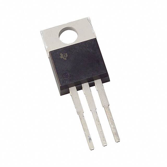
TO-220 (3)
TL783
BODY SIZE (NOM)
10.17 mm × 9.02 mm
10.16 mm × 8.70 mm
PFM (3)
9.40 mm × 8.00 mm
TO-263 (3)
10.18 mm × 8.41 mm
(1) For all available packages, see the orderable addendum at
the end of the data sheet.
4 Simplified Schematic
VI
−
Error
Amplifier
IN
æ R2 ö
VO » Vref ç 1 +
R1 ÷ø
è
+
VO
OUT
Protection
Circuit
Vref
R1
ADJ
R2
1
An IMPORTANT NOTICE at the end of this data sheet addresses availability, warranty, changes, use in safety-critical applications,
intellectual property matters and other important disclaimers. PRODUCTION DATA.
�TL783
SLVS036N – SEPTEMBER 1981 – REVISED JANUARY 2015
www.ti.com
Table of Contents
1
2
3
4
5
6
7
8
Features ..................................................................
Applications ...........................................................
Description .............................................................
Simplified Schematic.............................................
Revision History.....................................................
Pin Configuration and Functions .........................
Specifications.........................................................
1
1
1
1
2
3
4
7.1
7.2
7.3
7.4
7.5
7.6
4
4
4
4
5
6
Absolute Maximum Ratings ......................................
ESD Ratings..............................................................
Recommended Operating Conditions.......................
Thermal Information ..................................................
Electrical Characteristics...........................................
Typical Characteristics ..............................................
Detailed Description .............................................. 8
8.1 Overview ................................................................... 8
8.2 Functional Block Diagram ......................................... 8
8.3 Feature Description................................................... 8
8.4 Device Functional Modes.......................................... 8
9
Application and Implementation .......................... 9
9.1 Application Information.............................................. 9
9.2 Typical Application .................................................. 12
10 Power Supply Recommendations ..................... 16
11 Layout................................................................... 16
11.1 Layout Guidelines ................................................. 16
11.2 Layout Example .................................................... 16
12 Device and Documentation Support ................. 16
12.1 Trademarks ........................................................... 16
12.2 Electrostatic Discharge Caution ............................ 16
12.3 Glossary ................................................................ 16
13 Mechanical, Packaging, and Orderable
Information ........................................................... 16
5 Revision History
Changes from Revision M (April 2008) to Revision N
Page
•
Added Applications, Device Information table, Pin Functions table, ESD Ratings table, Thermal Information table,
Typical Characteristics, Feature Description section, Device Functional Modes, Application and Implementation
section, Power Supply Recommendations section, Layout section, Device and Documentation Support section, and
Mechanical, Packaging, and Orderable Information section. ................................................................................................. 1
•
Deleted Ordering Information table. ....................................................................................................................................... 1
2
Submit Documentation Feedback
Copyright © 1981–2015, Texas Instruments Incorporated
Product Folder Links: TL783
�TL783
www.ti.com
SLVS036N – SEPTEMBER 1981 – REVISED JANUARY 2015
6 Pin Configuration and Functions
KC (TO-220) PACKAGE
(TOP VIEW)
OUT
IN
OUT
ADJ
KTE (PowerFLEXTM) PACKAGE
(TOP VIEW)
OUT
IN
OUT
ADJ
KTT (TO-263) PACKAGE
(TOP VIEW)
OUT
IN
OUT
ADJ
Pin Functions
PIN
KC
TO-220
KTE
PowerFLEX™
KTT
TO-263
TYPE
ADJ
1
1
1
I/O
IN
3
3
3
I
Supply Input
OUT
2
2
2
O
Voltage Output
NAME
DESCRIPTION
Voltage adjustment pin. Connect a
resistor divider to determine the output
voltage.
Submit Documentation Feedback
Copyright © 1981–2015, Texas Instruments Incorporated
Product Folder Links: TL783
3
�TL783
SLVS036N – SEPTEMBER 1981 – REVISED JANUARY 2015
www.ti.com
7 Specifications
7.1 Absolute Maximum Ratings
over operating temperature range (unless otherwise noted) (1)
MIN
Vl – VO
Input-to-output differential voltage
TJ
Operating virtual junction temperature
Tstg
Storage temperature range
(1)
MAX
UNIT
125
V
150
°C
150
°C
–65
Stresses beyond those listed under Absolute Maximum Ratings may cause permanent damage to the device. These are stress ratings
only, and functional operation of the device at these or any other conditions beyond those indicated under Recommended Operating
Conditions is not implied. Exposure to absolute-maximum-rated conditions for extended periods may affect device reliability.
7.2 ESD Ratings
VALUE
V(ESD)
(1)
(2)
Electrostatic discharge
Human body model (HBM), per ANSI/ESDA/JEDEC JS-001, all pins (1)
2500
Charged device model (CDM), per JEDEC specification JESD22-C101,
all pins (2)
1000
UNIT
V
JEDEC document JEP155 states that 500-V HBM allows safe manufacturing with a standard ESD control process.
JEDEC document JEP157 states that 250-V CDM allows safe manufacturing with a standard ESD control process.
7.3 Recommended Operating Conditions
MIN
Vl – VO
Input-to-output differential voltage
IO
Output current
TJ
Operating virtual junction temperature
MAX
UNIT
125
V
15
700
mA
0
125
°C
7.4 Thermal Information
TL783
THERMAL METRIC (1)
KTE
KTT
KC
UNIT
3 PINS
RθJA
Junction-to-ambient thermal resistance
23
25.3
19
RθJC(top)
Junction-to-case (top) thermal resistance
N/A
18
17
RθJP
Junction-to-exposed-pad thermal resistance
2.7
1.94
3
(1)
4
°C/W
For more information about traditional and new thermal metrics, see the IC Package Thermal Metrics application report, SPRA953.
Submit Documentation Feedback
Copyright © 1981–2015, Texas Instruments Incorporated
Product Folder Links: TL783
�TL783
www.ti.com
SLVS036N – SEPTEMBER 1981 – REVISED JANUARY 2015
7.5 Electrical Characteristics
Vl – VO = 25 V, IO = 0.5 A, TJ = 0°C to 125°C (unless otherwise noted)
PARAMETER
TEST CONDITIONS (1)
TYP
MAX
TJ = 25°C
0.001
0.01
TJ = 0°C to 125°C
0.004
0.02
Input voltage regulation (2)
Vl – VO = 20 V to 125 V,
P ≤ rated dissipation
Ripple rejection
ΔVI(PP) = 10 V, VO = 10 V, f = 120 Hz
MIN
66
IO = 15 mA to 700 mA,
TJ = 25°C
25
VO ≥ 5 V
0.15%
0.5%
—
IO = 15 mA to 700 mA,
P ≤ rated dissipation
VO ≤ 5 V
20
70
mV
VO ≥ 5 V
0.3%
1.5%
0.4%
Output voltage long-term drift
1000 hours at TJ = 125°C, Vl – VO = 125 V
Output noise voltage
f = 10 Hz to 10 kHz, TJ = 25°C
Minimum output current to maintain regulation
Vl – VO = 125 V
0.003%
15
715
Vl – VO = 25 V, t = 30 ms
700
900
Vl – VO = 125 V, t = 30 ms
100
250
ADJ input current
Change in ADJ input current
Reference voltage (OUT to ADJ) (3)
Vl – VO = 10 V to 125 V, IO = 15 mA to 700 mA,
P ≤ rated dissipation
mA
1100
Vl – VO = 15 V, t = 30 ms
Vl – VO = 15 V to 125 V, IO = 15 mA to 700 mA,
P ≤ rated dissipation
mV
—
0.2%
Vl – VO = 25 V, t = 1 ms
(2)
(3)
dB
7.5
Output voltage change with temperature
(1)
%/V
VO ≤ 5 V
Output voltage regulation
Peak output current
76
UNIT
1.2
mA
83
110
μA
0.5
5
μA
1.27
1.3
V
Pulse-testing techniques maintain the junction temperature as close to the ambient temperature as possible. Thermal effects must be
taken into account separately.
Input voltage regulation is expressed here as the percentage change in output voltage per 1-V change at the input
Due to the dropout voltage and output current-limiting characteristics of this device, output current is limited to less than 700 mA at
input-to-output voltage differentials of less than 25 V.
Submit Documentation Feedback
Copyright © 1981–2015, Texas Instruments Incorporated
Product Folder Links: TL783
5
�TL783
SLVS036N – SEPTEMBER 1981 – REVISED JANUARY 2015
www.ti.com
7.6 Typical Characteristics
2
2
tw = 1 ms
1.8
1.6
Output Current Limit − (A)
Output Current Limit − (A)
1.6
1.4
1.2
TJ = 0°C
1
0.8
0.6
tw = 30 ms
1.8
TJ = 25°C
1.4
1.2
TJ = 0°C
1
0.8
TJ = 25°C
0.6
0.4
0.4
TJ = 125°C
TJ = 125°C
0.2
0.2
0
0
0
25
50
75
100
0
125
Figure 1. Output Current Limit
vs
Input-to-Output Voltage Differential
50
75
125
100
Figure 2. Output Current Limit
vs
Input-to-Output Voltage Differential
1.6
120
VI − VO = 25 V
TJ = 25°C
1.4
100
1.2
Ripple Rejection − (dB)
Output Current Limit − (A)
25
VI − VO − Input-to-Output Voltage Differential − (V)
VI − VO − Input-to-Output Voltage Differential − (V)
1
0.8
0.6
80
60
40
VI(AV) − VO = 25 V
DVI(PP) = 10 V
IO = 100 mA
f = 120 Hz
Co = 0
TJ = 25°C
0.4
20
0.2
0
0
10
0
20
30
0
40
10
20
30
40
50
60
70
80
90
100
VO − Output Voltage − (V)
Time − (ms)
Figure 4. Ripple Rejection
vs
Output Voltage
Figure 3. Output Current Limit
vs
Time
100
100
90
Ripple Rejection − dB
Ripple Rejection − (dB)
80
80
60
40
20
VI(AV) = 25 V
DVI(PP) = 10 V
VO = 10 V
f = 120 Hz
Co = 0
TJ = 25°C
100
200
50
40
Co = 0
30
10
300
400
500
600
700
800
IO − Output Current − (mA)
0
0.01
VI(AV) = 25 V
∆VI(PP) = 10 V
VO = 10 V
IO = 500 mA
TJ = 25°C
0.1
1
10
100
1000
f − Frequency − kHz
Figure 5. Ripple Rejection
vs
Output Current
6
Co = 10 µF
60
20
0
0
70
Figure 6. Ripple Rejection
vs
Frequency
Submit Documentation Feedback
Copyright © 1981–2015, Texas Instruments Incorporated
Product Folder Links: TL783
�TL783
www.ti.com
SLVS036N – SEPTEMBER 1981 – REVISED JANUARY 2015
Typical Characteristics (continued)
1.30
102
VI = 35 V
VO = 10 V
IO = 500 mA
TJ = 25°C
VI = 20 V
IO = 15 mA
1.29
V ref − Reference Voltage − (V)
Zo − Output Impedance − (W)
101
1
10−1
10−2
1.28
1.27
1.26
1.25
1.24
10−3
1.23
10−4
101
102
103
104
105
106
1.22
−75 −50 −25
107
25
90
VI = 25 V
VO = Vref
IO = 500 mA
Dropout Voltage − (V)
ADJ Input Current − (mA)
84
82
80
75
100 125 150 175
DVO = 100 mV
25
50
75
100
125
15
IO = 700 mA
IO = 600 mA
IO = 500 mA
10
IO = 250 mA
5
IO = 100 mA
IO = 15 mA
0
−75
−50
−25
0
25
75
50
100
TJ − Virtual Junction Temperature − (°C)
TJ − Virtual Junction Temperature − (°C)
Figure 9. Input Current at ADJ
vs
Virtual Junction Temperature
Figure 10. Dropout Voltage
vs
Virtual Junction Temperature
0
125
12
VI = 25 V
VO = 5 V
IO = 15 mA to 700 mA
−0.1
TJ = 0°C
10
I O − Output Current − (mA)
DVO − Output Voltage Deviation − (%)
50
20
86
0
25
Figure 8. Reference Voltage
vs
Virtual Junction Temperature
Figure 7. Output Impedance
vs
Frequency
88
0
TJ − Virtual Junction Temperature − (°C)
f − Frequency − (kHz)
−0.2
−0.3
−0.4
8
TJ = 25°C
6
TJ = 125°C
4
2
0
−0.5
0
25
50
75
100
125
0
150
25
50
75
100
125
VI − Input Voltage − (V)
TJ − Virtual Junction Temperature − (°C)
Figure 11. Output Voltage Deviation
vs
Virtual Junction Temperature
(1) This is the minimum current required to maintain voltage
regulation.
Figure 12. Output Current
vs
Input Voltage
Submit Documentation Feedback
Copyright © 1981–2015, Texas Instruments Incorporated
Product Folder Links: TL783
7
�TL783
SLVS036N – SEPTEMBER 1981 – REVISED JANUARY 2015
www.ti.com
8 Detailed Description
8.1 Overview
The TL783 device is an adjustable three-terminal high-voltage regulator with an output range of 1.25 V to 125 V
and a DMOS output transistor capable of sourcing more than 700 mA. It is designed for use in high-voltage
applications where standard bipolar regulators cannot be used. Excellent performance specifications, superior to
those of most bipolar regulators, are achieved through circuit design and advanced layout techniques.
As a state-of-the-art regulator, the TL783 device combines standard bipolar circuitry with high-voltage doublediffused MOS transistors on one chip, to yield a device capable of withstanding voltages far higher than standard
bipolar integrated circuits. Because of its lack of secondary-breakdown and thermal-runaway characteristics
usually associated with bipolar outputs, the TL783 maintains full overload protection while operating at up to
125 V from input to output. Other features of the device include current limiting, safe-operating-area (SOA)
protection, and thermal shutdown. Even if ADJ is disconnected inadvertently, the protection circuitry remains
functional.
Only two external resistors are required to program the output voltage. An input bypass capacitor is necessary
only when the regulator is situated far from the input filter. An output capacitor, although not required, improves
transient response and protection from instantaneous output short circuits. Excellent ripple rejection can be
achieved without a bypass capacitor at the adjustment terminal.
8.2 Functional Block Diagram
VI
−
IN
Error
Amplifier
æ R2 ö
VO » Vref ç 1 +
R1 ÷ø
è
+
VO
OUT
Protection
Circuit
Vref
R1
ADJ
R2
8.3 Feature Description
•
•
•
•
•
•
Output Adjustable From 1.25 V to 125 V when Used with an External Resistor Divider
700-mA Output Current
Full Short-Circuit, Safe-Operating-Area, and Thermal-Shutdown Protection
0.001%/V Typical Input Voltage Regulation
0.15% Typical Output Voltage Regulation
76-dB Typical Ripple Rejection
8.4 Device Functional Modes
8.4.1 Active Mode
The TL783 acts as a high-voltage adjustable regulator. The device works to keep the voltage at the OUT pin 1.25
V higher than the voltage at the ADJ pin. Therefore, a resistor divider can be used to set the output voltage.
8
Submit Documentation Feedback
Copyright © 1981–2015, Texas Instruments Incorporated
Product Folder Links: TL783
�TL783
www.ti.com
SLVS036N – SEPTEMBER 1981 – REVISED JANUARY 2015
9 Application and Implementation
NOTE
Information in the following applications sections is not part of the TI component
specification, and TI does not warrant its accuracy or completeness. TI’s customers are
responsible for determining suitability of components for their purposes. Customers should
validate and test their design implementation to confirm system functionality.
9.1 Application Information
9.1.1 General Configurations
VI = 145 to 200 V
7.5 kW, 1 W
TIP150
120 V, 1.5 W
IN
OUT
ADJ
R1
82 W
TL783
0.1 mF
125 V
+
10 mF
R2
8.2 kW, 2W
Figure 13. 125-V Short-Circuit-Protected Off-Line Regulator
VI = 70 to 125 V
10 W
TIP30C
TIPL762
1 kW
TL783
VO = 50 V
at 0.5 A
10 kW
IN
OUT
ADJ
82 W
+
50 mF
3.3 kW, 1W
Figure 14. 50-V Regulator With Current Boost
Submit Documentation Feedback
Copyright © 1981–2015, Texas Instruments Incorporated
Product Folder Links: TL783
9
�TL783
SLVS036N – SEPTEMBER 1981 – REVISED JANUARY 2015
www.ti.com
Application Information (continued)
125 V
1W
10 W
TIPL762
1 kW
TL783
10 kW
IN
OUT
æ R2 ö
VO = Vref ç 1 +
R1 ÷ø
è
ADJ
R1
82 W
+
50 mF
R2
Figure 15. Adjustable Regulator With Current Boost and Current Limit
VI
Load
I
V ref
R
TL783
IN
OUT
ADJ
R
Figure 16. Current-Sinking Regulator
10
Submit Documentation Feedback
Copyright © 1981–2015, Texas Instruments Incorporated
Product Folder Links: TL783
�TL783
www.ti.com
SLVS036N – SEPTEMBER 1981 – REVISED JANUARY 2015
Application Information (continued)
VI
TL783
1 mF
IN
OUT
ADJ
R
I=
V ref
R
Load
Figure 17. Current-Sourcing Regulator
VCC
TL783
1 mF
IN
OUT
ADJ
OUTPUT
82 W
R2
V+
−
+
INPUT
TL081
V−
æ R2 ö
VOFFSET = Vref ç I +
÷
è 82 ø
Figure 18. High-Voltage Unity-Gain Offset Amplifier
Submit Documentation Feedback
Copyright © 1981–2015, Texas Instruments Incorporated
Product Folder Links: TL783
11
�TL783
SLVS036N – SEPTEMBER 1981 – REVISED JANUARY 2015
www.ti.com
Application Information (continued)
VI = 90 V
TL783
IN
OUT
ADJ
6.25 W
TL783
IN
OUT
ADJ
82 W
48 V
3.9 kW
Figure 19. 48-V 200-mA Float Charger
9.2 Typical Application
The TL783 is typically used as an adjustable regulator.
æ R2 ö
VO = Vref ç 1 +
R1 ÷ø
è
TL783
IN
VI
OUT
ADJ
1 mF
(see Note A)
R1
82 W
+
+
10 mF
R2
0 to 8 kW
A.
Needed if device is more than 4 inches from filter capacitor
Figure 20. 1.25-V to 115-V Adjustable Regulator
9.2.1 Design Requirements
• Input and output decoupling capacitors for noise filtering.
• Resistor divider consisting of R1 and R2 to set the output voltage.
12
Submit Documentation Feedback
Copyright © 1981–2015, Texas Instruments Incorporated
Product Folder Links: TL783
�TL783
www.ti.com
SLVS036N – SEPTEMBER 1981 – REVISED JANUARY 2015
Typical Application (continued)
9.2.2 Detailed Design Procedure
The internal reference (see Simplified Schematic) generates 1.25 V nominal (Vref) between OUT and ADJ. This
voltage is developed across R1 and causes a constant current to flow through R1 and the programming resistor
R2, giving an output voltage of:
VO = Vref (1 + R2 / R1) + lI(ADJ) (R2)
or
VO ≉ Vref (1 + R2 / R1)
The TL783 was designed to minimize the input current at ADJ and maintain consistency over line and load
variations, thereby minimizing the associated (R2) error term.
To maintain II(ADJ) at a low level, all quiescent operating current is returned to the output terminal. This quiescent
current must be sunk by the external load and is the minimum load current necessary to prevent the output from
rising. The recommended R1 value of 82 Ω provides a minimum load current of 15 mA. Larger values can be
used when the input-to-output differential voltage is less than 125 V (see the output-current curve in Figure 12) or
when the load sinks some portion of the minimum current.
9.2.2.1 Bypass Capacitors
The TL783 regulator is stable without bypass capacitors; however, any regulator becomes unstable with certain
values of output capacitance if an input capacitor is not used. Therefore, the use of input bypassing is
recommended whenever the regulator is located more than four inches from the power-supply filter capacitor. A
1-μF tantalum or aluminum electrolytic capacitor usually is sufficient.
Adjustment-terminal capacitors are not recommended for use on the TL783 because they can seriously degrade
load transient response, as well as create a need for extra protection circuitry. Excellent ripple rejection presently
is achieved without this added capacitor.
Due to the relatively low gain of the MOS output stage, output voltage dropout may occur under large-load
transient conditions. The addition of an output bypass capacitor greatly enhances load transient response and
prevents dropout. For most applications, it is recommended that an output bypass capacitor be used, with a
minimum value of:
Co (μF) = 15 / VO
Larger values provide proportionally better transient-response characteristics.
Submit Documentation Feedback
Copyright © 1981–2015, Texas Instruments Incorporated
Product Folder Links: TL783
13
�TL783
SLVS036N – SEPTEMBER 1981 – REVISED JANUARY 2015
www.ti.com
Typical Application (continued)
9.2.2.2 Protection Circuitry
The TL783 regulator includes built-in protection circuits capable of guarding the device against most overload
conditions encountered in normal operation. These protective features are current limiting, safe-operating-area
protection, and thermal shutdown. These circuits protect the device under occasional fault conditions only.
Continuous operation in the current limit or thermal shutdown mode is not recommended.
The internal protection circuits of the TL783 protect the device up to maximum-rated VI as long as certain
precautions are taken. If Vl is switched on instantaneously, transients exceeding maximum input ratings may
occur, which can destroy the regulator. Usually, these are caused by lead inductance and bypass capacitors
causing a ringing voltage on the input. In addition, when rise times in excess of 10 V/ns are applied to the input,
a parasitic npn transistor in parallel with the DMOS output can be turned on, causing the device to fail. If the
device is operated over 50 V and the input is switched on, rather than ramped on, a low-Q capacitor, such as
tantalum or aluminum electrolytic, should be used, rather than ceramic, paper, or plastic bypass capacitors. A Q
factor of 0.015, or greater, usually provides adequate damping to suppress ringing. Normally, no problems occur
if the input voltage is allowed to ramp upward through the action of an ac line rectifier and filter network.
Similarly, when an instantaneous short circuit is applied to the output, both ringing and excessive fall times can
result. A tantalum or aluminum electrolytic bypass capacitor is recommended to eliminate this problem. However,
if a large output capacitor is used, and the input is shorted, addition of a protection diode may be necessary to
prevent capacitor discharge through the regulator. The amount of discharge current delivered is dependent on
output voltage, size of capacitor, and fall time of Vl. A protective diode (see Figure 21) is required only for
capacitance values greater than:
Co (μF) = 3 × 10⁴ / (VO)2
Care always should be taken to prevent insertion of regulators into a socket with power on. Power should be
turned off before removing or inserting regulators.
TL783
VI
IN
OUT
VO
ADJ
R1
Co
R2
Figure 21. Regulator With Protective Diode
14
Submit Documentation Feedback
Copyright © 1981–2015, Texas Instruments Incorporated
Product Folder Links: TL783
�TL783
www.ti.com
SLVS036N – SEPTEMBER 1981 – REVISED JANUARY 2015
Typical Application (continued)
9.2.2.3 Load Regulation
The current-set resistor (R1) should be located close to the regulator output terminal, rather than near the load.
This eliminates long line drops from being amplified, through the action of R1 and R2, to degrade load regulation.
To provide remote ground sensing, R2 should be near the load ground.
VO
TL783
VI
IN
Rline
OUT
ADJ
RL
R1
R2
Figure 22. Regulator With Current-Set Resistor
D VO − Output Voltage Deviation − (V)
TJ = 25°C
Co = 0
0.4
0.2
Co = 10 mF
0
−0.2
1
0.5
0
0
1
2
3
4
Time − (ms)
I O − Output Current − (A)
Change in Input Voltage − (V) D VO − Output Voltage Deviation − (V)
9.2.3 Application Curves
6
4
2
0
−2
−4
−6
0.8
VI = 35 V
VO = 10 V
Co = 1 mF
TJ = 25°C
0.6
0.4
0.2
0
Figure 23. Line Transient Response
0
40
80
120
160
200
Submit Documentation Feedback
Copyright © 1981–2015, Texas Instruments Incorporated
Product Folder Links: TL783
240
Time − (ms)
Figure 24. Load Transient Response
15
�TL783
SLVS036N – SEPTEMBER 1981 – REVISED JANUARY 2015
www.ti.com
10 Power Supply Recommendations
A decoupling capacitor is needed on the IN pin of the TL783 if the TL783 is more than 4 inches from its power
supply's filter capacitor. The differential input and output voltage levels are detailed in Recommended Operating
Conditions.
11 Layout
11.1 Layout Guidelines
Input and output traces should be thick enough to handle desired currents, which can reach up to 700 mA on the
output. ADJ pin traces can be smaller because the adjustment current is negligible.
11.2 Layout Example
Ground
OUTPUT
R2
Power
INPUT
OUTPUT
ADJ/GND
R1
Cadj
Ground
Figure 25. Layout Example
12 Device and Documentation Support
12.1 Trademarks
All trademarks are the property of their respective owners.
12.2 Electrostatic Discharge Caution
These devices have limited built-in ESD protection. The leads should be shorted together or the device placed in conductive foam
during storage or handling to prevent electrostatic damage to the MOS gates.
12.3 Glossary
SLYZ022 — TI Glossary.
This glossary lists and explains terms, acronyms, and definitions.
13 Mechanical, Packaging, and Orderable Information
The following pages include mechanical, packaging, and orderable information. This information is the most
current data available for the designated devices. This data is subject to change without notice and revision of
this document. For browser-based versions of this data sheet, refer to the left-hand navigation.
16
Submit Documentation Feedback
Copyright © 1981–2015, Texas Instruments Incorporated
Product Folder Links: TL783
�PACKAGE OPTION ADDENDUM
www.ti.com
13-Aug-2021
PACKAGING INFORMATION
Orderable Device
Status
(1)
Package Type Package Pins Package
Drawing
Qty
Eco Plan
(2)
Lead finish/
Ball material
MSL Peak Temp
Op Temp (°C)
Device Marking
(3)
(4/5)
(6)
TL783CKCSE3
ACTIVE
TO-220
KCS
3
50
RoHS & Green
SN
N / A for Pkg Type
0 to 125
TL783C
TL783CKTTR
ACTIVE
DDPAK/
TO-263
KTT
3
500
RoHS & Green
SN
Level-3-245C-168 HR
0 to 125
TL783C
TL783CKTTRG3
ACTIVE
DDPAK/
TO-263
KTT
3
500
RoHS & Green
SN
Level-3-245C-168 HR
0 to 125
TL783C
(1)
The marketing status values are defined as follows:
ACTIVE: Product device recommended for new designs.
LIFEBUY: TI has announced that the device will be discontinued, and a lifetime-buy period is in effect.
NRND: Not recommended for new designs. Device is in production to support existing customers, but TI does not recommend using this part in a new design.
PREVIEW: Device has been announced but is not in production. Samples may or may not be available.
OBSOLETE: TI has discontinued the production of the device.
(2)
RoHS: TI defines "RoHS" to mean semiconductor products that are compliant with the current EU RoHS requirements for all 10 RoHS substances, including the requirement that RoHS substance
do not exceed 0.1% by weight in homogeneous materials. Where designed to be soldered at high temperatures, "RoHS" products are suitable for use in specified lead-free processes. TI may
reference these types of products as "Pb-Free".
RoHS Exempt: TI defines "RoHS Exempt" to mean products that contain lead but are compliant with EU RoHS pursuant to a specific EU RoHS exemption.
Green: TI defines "Green" to mean the content of Chlorine (Cl) and Bromine (Br) based flame retardants meet JS709B low halogen requirements of


 工商网监
湘ICP备2023018690号
工商网监
湘ICP备2023018690号
