TLC5944
TL
C5
94
4
TL
C5
944
www.ti.com .............................................................................................................................................................. SBVS112A – JUNE 2008 – REVISED JULY 2009
16-Channel, 12-Bit PWM LED Driver with
6-Bit Dot Correction and Pre-Charge FET
FEATURES
1
• 16 Channels, Constant Current Sink Output
• 60-mA Capability (Constant Current Sink)
• 12-Bit (4096 Steps) Grayscale Control with
PWM
• 6-Bit (64 Steps) Dot Correction with Sink
Current
• Internal Pre-Charge FET to Prevent LED
Ghosting Phenomenon on Multiplexed LED
Systems
• LED Power-Supply Voltage up to 15 V
• VCC = 3.0 V to 5.5 V
• Constant Current Accuracy:
– Channel-to-Channel = ±1%
– Device-to-Device = ±3%
• CMOS Logic Level I/O
• 30-MHz Data Transfer Rate
• 33-MHz Grayscale Control Clock
• Continuous Base LED Open Detection (LOD):
– Detect LED opening and LED short to GND
during display with auto output off function
•
23
Thermal Shutdown (TSD):
– Automatic shutdown at over-temperature
conditions
– Restart under normal temperature
Pre-Thermal Warning (PTW):
– High temperature operation alert
Readable Error Information:
– LED Open Detection (LOD)
– Thermal Error Flag (TEF)
– Pre-Thermal Warning (PTW)
Noise Reduction:
– 4-channel grouped delay to prevent inrush
current
Operating Temperature: –40°C to +85°C
•
•
•
•
APPLICATIONS
•
Monochrome, Multicolor, Full-Color LED
Displays Using Multiplexing System
LED Signboards Using Multiplexing System
•
VLED
LINEn
VLED
LINE0
ROWSEL0
ROWSELn
¼
OUT0
DATA
SCLK
DCSEL
SCLK
XERR
VLED
VCC
VCC
SOUT
XERR
VLED
VUP
BLANK
VCC
GSCLK
VCC
IREF
RIREF
OUT15
SCLK
XLAT
GSCLK
FLAGS
READ
¼
SIN
DCSEL
VUP
BLANK
GSCLK
XERR
READ
SOUT
XLAT
BLANK
OUT0
OUT15
DCSEL
XLAT
Controller
¼
SIN
TLC5944
IC1
GND
VCC
IREF
RIREF
TLC5944
ICn
GND
5
Typical Application Circuit (Multiple Daisy-Chained TLC5944s)
1
2
3
Please be aware that an important notice concerning availability, standard warranty, and use in critical applications of Texas
Instruments semiconductor products and disclaimers thereto appears at the end of this data sheet.
PowerPAD is a trademark of Texas Instruments, Incorporated.
All other trademarks are the property of their respective owners.
PRODUCTION DATA information is current as of publication date.
Products conform to specifications per the terms of the Texas
Instruments standard warranty. Production processing does not
necessarily include testing of all parameters.
Copyright © 2008–2009, Texas Instruments Incorporated
�TLC5944
SBVS112A – JUNE 2008 – REVISED JULY 2009 .............................................................................................................................................................. www.ti.com
DESCRIPTION
The TLC5944 is a 16-channel, constant current sink driver. Each channel is individually adjustable with 4096
pulse-width modulated (PWM) steps and 64 constant sink current (dot correction) steps. The dot correction (DC)
adjusts for brightness variations between LEDs. Both grayscale (GS) control and DC are accessible via a
common serial interface port. The maximum current value of all 16 channels can be set by a single external
resistor.
The TLC5944 has an internal pre-charge FET to prevent the ghost-lighting phenomenon that occurs on
multiplexed LED systems. The TLC5944 has three error detection circuits for LED open detection (LOD), a
thermal error flag (TEF), and a pre-thermal warning (PTW). The LOD detects a broken or disconnected LED, and
a shorted LED to GND during the display period. The TEF indicates a too-high temperature condition; when the
TEF is set, all output drivers are turned off by the thermal shutdown (TSD) protection. Additionally, when the TEF
is cleared, all output drivers are restarted. The PTW indicates that the IC is operating in a high temperature
condition. The output drivers remain on when PTW is set.
blank
This integrated circuit can be damaged by ESD. Texas Instruments recommends that all integrated circuits be handled with
appropriate precautions. Failure to observe proper handling and installation procedures can cause damage.
ESD damage can range from subtle performance degradation to complete device failure. Precision integrated circuits may be more
susceptible to damage because very small parametric changes could cause the device not to meet its published specifications.
PACKAGE/ORDERING INFORMATION (1)
(1)
PRODUCT
PACKAGE-LEAD
TLC5944
HTSSOP-28 PowerPAD™
TLC5944
5 mm × 5 mm QFN-32
ORDERING NUMBER
TRANSPORT MEDIA,
QUANTITY
TLC5944PWPR
Tape and Reel, 2000
TLC5944PWP
Tube, 50
TLC5944RHBR
Tape and Reel, 3000
TLC5944RHBT
Tape and Reel, 250
For the most current package and ordering information see the Package Option Addendum at the end of this document, or see the TI
web site at www.ti.com.
ABSOLUTE MAXIMUM RATINGS (1) (2)
Over operating free-air temperature range, unless otherwise noted.
PARAMETER
TLC5944
UNIT
V
VCC
Supply voltage, VCC
–0.3 to +6.0
VUP
Pre-charge voltage
–0.3 to +16
V
XERR
6
mA
OUT0 to OUT15
70
mA
–0.3 to VCC + 0.3
V
SOUT, XERR
–0.3 to VCC + 0.3
V
OUT0 to OUT15
–0.3 to VUP + 0.3
V
+150
°C
–55 to +150
°C
2
kV
500
V
IOUT
Output current (dc)
VIN
Input voltage range:
SIN, SCLK, XLAT, BLANK, GSCLK, DCSEL, IREF
VOUT
Output voltage range
TJ(max)
Operating junction temperature
TSTG
Storage temperature range
ESD rating
(1)
(2)
2
Human body model (HBM)
Charged device model (CDM)
Stresses above these ratings may cause permanent damage. Exposure to absolute maximum conditions for extended periods may
degrade device reliability. These are stress ratings only, and functional operation of the device at these or any other conditions beyond
those specified is not supported.
All voltage values are with respect to network ground terminal.
Submit Documentation Feedback
Copyright © 2008–2009, Texas Instruments Incorporated
Product Folder Link(s): TLC5944
�TLC5944
www.ti.com .............................................................................................................................................................. SBVS112A – JUNE 2008 – REVISED JULY 2009
RECOMMENDED OPERATING CONDITIONS
At TA= –40°C to +85°C, unless otherwise noted.
TLC5944
PARAMETER
TEST CONDITIONS
MIN
NOM
MAX
UNIT
DC Characteristics: VCC = 3 V to 5.5 V
VCC
Supply voltage
3.0
5.5
V
VUP
Pre-charge voltage
3.0
15
V
VO
Voltage applied to output
VUP
V
VIH
High-level input voltage
0.7 × VCC
VCC
V
VIL
Low-level input voltage
GND
0.3 × VCC
IOH
High-level output current
IOL
Low-level output current
IOLC
Constant output sink current
TA
Operating free-air temperature
TJ
Operating junction
temperature
OUT0 to OUT15
V
SOUT
–1
mA
SOUT
1
mA
XERR
5
mA
OUT0 to OUT15
60
mA
–40
+85
°C
–40
+125
°C
AC Characteristics: VCC = 3 V to 5.5 V
fCLK (sclk)
Data shift clock frequency
fCLK (gsclk)
Grayscale control clock
frequency
TWH0/TWL0
Pulse duration
TWH1
SCLK
30
MHz
GSCLK
33
MHz
SCLK, GSCLK
10
ns
XLAT, BLANK
15
ns
TSU0
SIN–SCLK↑
5
ns
TSU1
BLANK↓–GSCLK↑
15
ns
XLAT↑–SCLK↑
100
ns
XLAT↓–SCLK↑
(for SID reading only)
20
ns
TSU4
DCSEL–SCLK↑
10
ns
TSU5
DCSEL–XLAT↑
10
ns
TH0
SIN–SCLK↑
3
ns
TH1
XLAT↑–SCLK↑
10
ns
DCSEL–SCLK↓
10
ns
DCSEL–XLAT↑
100
ns
TSU2
Setup time
TSU3
Hold time
TH2
TH3
DISSIPATION RATINGS
PACKAGE
OPERATING FACTOR
ABOVE TA = +25°C
TA < +25°C
POWER RATING
TA = +70°C
POWER RATING
TA = +85°C
POWER RATING
HTSSOP-28 with
PowerPAD soldered (1)
31.67 mW/°C
3958 mW
2533 mW
2058 mW
HTSSOP-28 with
PowerPAD not soldered (2)
16.21 mW/°C
2026 mW
1296 mW
1053 mW
27.86 mW/°C
3482 mW
2228 mW
1811 mW
QFN-32
(1)
(2)
(3)
(3)
With PowerPAD soldered onto copper area on printed circuit board (PCB); 2-oz. copper. For more information, see SLMA002 (available
for download at www.ti.com).
With PowerPAD not soldered onto copper area on PCB.
The package thermal impedance is calculated in accordance with JESD51-5.
Submit Documentation Feedback
Copyright © 2008–2009, Texas Instruments Incorporated
Product Folder Link(s): TLC5944
3
�TLC5944
SBVS112A – JUNE 2008 – REVISED JULY 2009 .............................................................................................................................................................. www.ti.com
ELECTRICAL CHARACTERISTICS
At VCC = 3.0 V to 5.5 V and TA = –40°C to +85°C. Typical values at VCC = 3.3 V and TA = +25°C, unless otherwise noted.
TLC5944
PARAMETER
VOH
TEST CONDITIONS
High-level output voltage
VOL
Low-level output voltage
IIN
MAX
UNIT
VCC – 0.4
VCC
V
IOL = 1 mA at SOUT
0
0.4
V
IOL = 5 mA at XERR
0
0.4
V
–1
1
µA
IOH = –1 mA at SOUT
VIN = VCC or GND at SIN, SCLK, XLAT, GSCLK,
BLANK, DCSEL
Input current
MIN
TYP
ICC1
SIN/SCLK/GSCLK/XLAT/DCSEL = low, BLANK = high,
DCn = 3Fh, VOUTn = 1 V, RIREF = 24 kΩ
1
2
mA
ICC2
SIN/SCLK/GSCLK/XLAT/DCSEL = low, BLANK = high,
DCn = 3Fh, VOUTn = 1 V, RIREF = 1.6 kΩ
5
10
mA
ICC3
SCLK = 30 MHz, GSCLK = 33 MHz, SIN = 15 MHz,
XLAT/DCSEL = low,
BLANK = low during 4095 GSCLK period and high
during 1 GSCLK period,
GSn = FFFh, DCn = 3Fh, VOUTn = 1 V,
RIREF = 1.6 kΩ
17
35
mA
SCLK = 30 MHz, GSCLK = 33 MHz, SIN = 15 MHz,
XLAT/DCSEL = low,
BLANK = low during 4095 GSCLK period and high
during 1 GSCLK period,
GSn = FFFh, DCn = 3Fh, VOUTn = 1 V,
RIREF = 820 Ω
30
60
mA
60
66
mA
All OUTn for constant current driver, all output off,
BLANK = high, VOUTn = VOUTfix = 15 V, VUP = 15 V,
RIREF = 820 Ω (see Figure 10), at OUT0 to OUT15
0.1
µA
All OUTn for pre-charge FET, all output off,
BLANK = low, VOUTn = VOUTfix = 0 V, VUP = 15 V,
RIREF = 820 Ω (see Figure 10), at OUT0 to OUT15
–10
µA
1
µA
Supply current (VCC)
ICC4
IO(LC)
Constant output current
IO(LKG)
Leakage output current
IO(LKG1)
IO(LKG2)
All OUTn = ON, DCn = 3Fh, VOUTn = VOUTfix = 1 V,
RIREF = 1 kΩ (see Figure 9), at OUT0 to OUT15
54
XERR, no error status, VOUTn = 5.5 V
ΔIO(LC)
Constant current error
(channel-to-channel) (1)
All OUTn = ON, DCn = 3Fh, VOUTn = 1 V,
RIREF = 820 Ω, at OUT0 to OUT15
±1
±3
%
ΔIO(LC1)
Constant current error
(device-to-device) (2)
All OUTn = ON, DCn = 3Fh, VOUTn = 1 V,
RIREF = 820 Ω, at OUT0 to OUT15
±3
±6
%
ΔIO(LC2)
Line regulation (3)
All OUTn = ON, DCn = 3Fh, VOUTn = 1 V,
RIREF = 820 Ω, at OUT0 to OUT15
±0.5
±1
%/V
(1)
The deviation of each output from the average of OUT0–OUT15 constant current. Deviation is calculated by the formula:
IOUTn
D (%) =
-1
´ 100
(IOUT0 + IOUT1 + ... + IOUT14 + IOUT15)
(2)
16
.
The deviation of the OUT0–OUT15 constant current average from the ideal constant current value.
Deviation is calculated by the following formula:
(IOUT0 + IOUT1 + ... IOUT14 + IOUT15)
- (Ideal Output Current)
16
D (%) =
´ 100
Ideal Output Current
Ideal current is calculated by the formula:
1.20
IOUT(IDEAL) = 40.5 ´
(3)
RIREF
Line regulation is calculated by this equation:
D (%/V) =
(IOUTn at VCC = 5.5 V) - (IOUTn at VCC = 3.0 V)
4
100
´
(IOUTn at VCC = 3.0 V)
5.5 V - 3 V
Submit Documentation Feedback
Copyright © 2008–2009, Texas Instruments Incorporated
Product Folder Link(s): TLC5944
�TLC5944
www.ti.com .............................................................................................................................................................. SBVS112A – JUNE 2008 – REVISED JULY 2009
ELECTRICAL CHARACTERISTICS (continued)
At VCC = 3.0 V to 5.5 V and TA = –40°C to +85°C. Typical values at VCC = 3.3 V and TA = +25°C, unless otherwise noted.
TLC5944
PARAMETER
TEST CONDITIONS
MIN
All OUTn = ON, DCn = 3Fh, VOUTn = 1 V to 3 V,
RIREF = 820 Ω, at OUT0 to OUT15
(4)
ΔIO(LC3)
Load regulation
RPCHG
Pre-charge FET on-resistance
VUP = 3 V, VOUTn = 1 V, BLANK = high,
OUT0 to OUT15
(5)
TYP
MAX
UNIT
±1
±3
%/V
1
3
kΩ
T(TEF)
Thermal error flag threshold
Junction temperature
+150
+162
+175
°C
T(HYST)
Thermal error flag hysteresis
Junction temperature (5)
+5
+10
+20
°C
T(PTW)
Pre-thermal warning threshold
Junction temperature (5)
+105
+120
+135
°C
T(HYSP)
Pre-thermal warning hysteresis
Junction temperature (5)
+5
+10
+20
°C
VLOD
LED open detection threshold
All OUTn = ON
0.2
0.3
0.4
V
VIREF
Reference voltage output
RIREF = 820 Ω
1.16
1.20
1.24
V
(4)
Load regulation is calculated by the equation:
D (%/V) =
(IOUTn at VOUTn = 3 V) - (IOUTn at VOUTn = 1 V)
(5)
100
´
(IOUTn at VOUTn = 1 V)
3V-1V
Not tested. Specified by design.
SWITCHING CHARACTERISTICS
At VCC = 3.0 V to 5.5 V, TA = –40°C to +85°C, CL = 15 pF, RL = 68 Ω, RIREF = 820 Ω, VLED = 5.0 V, and VUP = 5.0 V. Typical
values at VCC = 3.3 V and TA = +25°C, unless otherwise noted.
TLC5944
PARAMETER
tR0
TEST CONDITIONS
TYP
SOUT (see Figure 6)
Rise time
tR1
MIN
16
OUTn, DCn = 3Fh (see Figure 5)
tF0
SOUT (see Figure 6)
tF1
OUTn, DCn = 3Fh (see Figure 5)
Fall time
MAX
10
30
16
10
30
UNIT
ns
ns
tF2
XERR, CL XERR = 100 pF, RL XERR = 1 kΩ,
VXERR = 5 V (see Figure 7)
50
ns
tD0
SCLK↑ to SOUT
25
ns
tD1
DCSEL to SOUT
25
ns
tD2
BLANK↑ to OUT0 sink current off
20
40
ns
tD3
GSCLK↑ to OUT0/4/8/12
5
18
40
ns
tD4
GSCLK↑ to OUT1/5/9/13
20
42
73
ns
tD5
GSCLK↑ to OUT2/6/10/14
35
66
106
ns
tD6
GSCLK↑ to OUT3/7/11/15
50
90
140
ns
tD7
XLAT↑ to IOUT (dot correction)
50
ns
tD8
BLANK↑ to pre-charge FET on, RL PRE = 10 kΩ,
constant current driver off (see Figure 8)
130
ns
10
ns
Propagation delay time
tON_ERR
(1)
Output on-time error
(1)
GSn = 001h, GSCLK = 33 MHz
10
–20
35
Output on-time error is calculated by the following formula: TON_ERR (ns) = tOUTON – TGSCLK. tOUTON is the actual on-time of the constant
current driver. TGSCLK is the period of GSCLK.
Submit Documentation Feedback
Copyright © 2008–2009, Texas Instruments Incorporated
Product Folder Link(s): TLC5944
5
�TLC5944
SBVS112A – JUNE 2008 – REVISED JULY 2009 .............................................................................................................................................................. www.ti.com
FUNCTIONAL BLOCK DIAGRAM
XERR
VUP
VCC
33rd GSCLK Signal
After BLANK Goes Low
VUP
XERR
Control
16
LED Open Detection Data Latch
(16 LOD)
VCC
16
LSB
MSB
SIN
Grayscale Shift Register
(12 Bits x 16 Channels)
0
SOUT
191
192
SCLK
LSB
MSB
Grayscale Data Latch
(12 Bits x 16 Channels)
XLAT
0
191
LSB
MSB
Dot Correction Shift Register
(6 Bits x 16 Channels)
0
95
192
96
MSB
DCSEL
95
0
Grayscale
Counter
GSCLK
+120°C Warning
Dot Correction Data Latch
(6 Bits x 16 Channels)
12
+162°C Warning
LSB
12-Bit PWM Timing Control
16
BLANK
96
Thermal
Detection
and
Flag Control
(+162°C/+120°C)
Output Switching Delay
(4-Channel Unit)
16
Reference
Current
Control
IREF
Constant Current Sink Driver With Dot Correction
(16 Channels)
16
LED Open Detection
(LOD, 16 Channels)
GND
VUP
GND
Pre-Charge FET
(16 Channels)
OUT0
6
OUT1
¼
OUT14
OUT15
Submit Documentation Feedback
Copyright © 2008–2009, Texas Instruments Incorporated
Product Folder Link(s): TLC5944
�TLC5944
www.ti.com .............................................................................................................................................................. SBVS112A – JUNE 2008 – REVISED JULY 2009
DEVICE INFORMATION
PWP PACKAGE
HTSSOP-28 PowerPAD
(TOP VIEW)
GSCLK
SOUT
XERR
OUT15
OUT14
OUT13
OUT12
OUT11
24
23
22
21
20
19
18
17
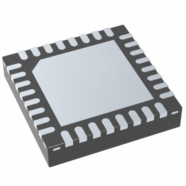
RHB PACKAGE
5mm × 5mm QFN-32
(TOP VIEW)
GND
1
28
VCC
BLANK
2
27
IREF
XLAT
3
26
VUP
SCLK
4
25
GSCLK
VUP
25
16
OUT10
SIN
5
24
SOUT
IREF
26
15
OUT9
DCSEL
6
23
XERR
VCC
27
14
OUT8
OUT0
7
22
OUT15
NC
28
13
NC
12
NC
Thermal
PAD
Thermal
Pad
31
10
OUT6
OUT4
11
18
OUT11
XLAT
32
9
OUT5
OUT5
12
17
OUT10
OUT6
13
16
OUT9
OUT7
14
15
OUT8
8
BLANK
OUT4
OUT12
7
19
OUT3
10
6
OUT3
OUT2
OUT7
5
11
OUT1
30
4
GND
OUT0
OUT13
3
20
DCSEL
9
OUT2
2
29
SIN
NC
1
OUT14
8
SCLK
21
OUT1
NC = No internal connection.
Submit Documentation Feedback
Copyright © 2008–2009, Texas Instruments Incorporated
Product Folder Link(s): TLC5944
7
�TLC5944
SBVS112A – JUNE 2008 – REVISED JULY 2009 .............................................................................................................................................................. www.ti.com
TERMINAL FUNCTIONS
TERMINAL
NAME
SIN
PWP
RHB
I/O
5
2
I
Serial data input for grayscale and dot correction.
DESCRIPTION
SCLK
4
1
I
Serial data shift clock for GS shift register and DC shift register. Schmitt buffer input. The shift
register is selected by the DCSEL pin. Data present on the SIN pin are shifted into the shift
register selected by DCSEL with the rising edge of the SCLK pin. Data in the selected shift
register are shifted to the MSB side by 1-bit synchronizing to the rising edge of SCLK. The MSB
data of the selected register appears on SOUT.
XLAT
3
32
I
Data in the GS and DC shift register are moved to the respective data latch with a low-to-high
transition of this pin.
DCSEL
6
3
I
Shift register and data latch select. When DCSEL is low, SCLK/XLAT/SOUT are connected to the
GS shift register and data latch. When DCSEL is high, SCLK/XLAT/SOUT are connected to the
DC shift register and data latch. DCSEL should not be changed while SCLK is high.
GSCLK
25
24
I
Reference clock for grayscale PWM control. If BLANK is low, then each rising edge of GSCLK
increments the grayscale counter for PWM control.
BLANK
2
31
I
Blank (all constant current outputs off). When BLANK is high, all constant current outputs (OUT0
through OUT15) are forced off, the grayscale counter is reset to '0', and the grayscale PWM
timing controller is initialized. When BLANK is low, all constant current outputs are controlled by
the grayscale PWM timing controller.
IREF
27
26
I/O
Constant current value setting. OUT0 through OUT15 sink constant current is set to the desired
value by connecting an external resistor between IREF and GND.
SOUT
24
23
O
Serial data output for GS, DC, and status information data (SID). This output is connected to the
MSB of the shift register selected by DCSEL.
XERR
23
22
O
Error output. Open-drain output. XERR goes low when LOD or TEF are set. XERR is in high
impedance when error free.
OUT0
7
4
O
Constant current output. Each output can be tied to other outputs to increase the constant
current.
OUT1
8
5
O
Constant current output
OUT2
9
6
O
Constant current output
OUT3
10
7
O
Constant current output
OUT4
11
8
O
Constant current output
OUT5
12
9
O
Constant current output
OUT6
13
10
O
Constant current output
OUT7
14
11
O
Constant current output
OUT8
15
14
O
Constant current output
OUT9
16
15
O
Constant current output
OUT10
17
16
O
Constant current output
OUT11
18
17
O
Constant current output
OUT12
19
18
O
Constant current output
OUT13
20
19
O
Constant current output
OUT14
21
20
O
Constant current output
OUT15
22
21
O
Constant current output
VCC
28
27
—
Power-supply voltage
VUP
26
25
—
Pre-charge FET power supply
GND
1
30
—
Power ground
—
12, 13,
28, 29
—
No internal connection
NC
8
Submit Documentation Feedback
Copyright © 2008–2009, Texas Instruments Incorporated
Product Folder Link(s): TLC5944
�TLC5944
www.ti.com .............................................................................................................................................................. SBVS112A – JUNE 2008 – REVISED JULY 2009
PARAMETER MEASUREMENT INFORMATION
PIN EQUIVALENT INPUT AND OUTPUT SCHEMATIC DIAGRAMS
VCC
VCC
INPUT
SOUT
GND
GND
Figure 1. SIN, SCLK, XLAT, DCSEL, BLANK, GSCLK
Figure 2. SOUT
XERR
OUTn
GND
GND
Figure 3. XERR
Figure 4. OUT0 Through OUT15
TEST CIRCUITS
RL
VCC
VCC
VCC
OUTn
IREF
VLED
(1)
RIREF
SOUT
VCC
CL
GND
(1)
(1)
CL includes measurement probe and jig
capacitance.
Figure 5. Rise Time and Fall Time Test Circuit for OUTn
VCC
(1)
CL includes measurement probe and jig
capacitance.
Figure 6. Rise Time and Fall Time Test Circuit for SOUT
RL XERR
VCC
VUP
VCC
XERR
CL XERR
GND
CL
GND
(1)
VCC
VUP
VXERR
OUTn
RL PRE
GND
(1) CL
XERR
Figure 8. Delay Time Test Circuit for Pre-Charge FET
includes measurement probe and jig capacitance.
Figure 7. Fall Time Test Circuit for XERR
VCC
OUT0
VCC
IREF
VCC
IREF
GND OUT15
VOUTn
RIREF
VOUTFIX
Figure 9. Constant Current Test Circuit for OUTn
VUP
OUT0
OUTn
¼
¼
RIREF
VUP
OUTn
¼
¼
VCC
CL
GND OUT15
VOUTn
VOUTFIX
Figure 10. Leakage Current of Pre-Charge FET Test
Circuit for OUTn
Submit Documentation Feedback
Copyright © 2008–2009, Texas Instruments Incorporated
Product Folder Link(s): TLC5944
9
�TLC5944
SBVS112A – JUNE 2008 – REVISED JULY 2009 .............................................................................................................................................................. www.ti.com
TIMING DIAGRAMS
TWH0, TWL0, TWH1:
VCC
INPUT
(1)
50%
GND
TWH
TWL
TSU0, TSU1, TSU2, TSU3, TSU4, TSU5, TH0, TH1, TH2, TH3:
VCC
CLOCK
INPUT
(1)
50%
GND
TSU
TH
VCC
DATA/CONTROL
INPUT
(1)
50%
GND
(1)
Input pulse rise and fall time is 1 ns to 3 ns.
Figure 11. Input Timing
tR0, tR1, tF0, tF1, tF2, tD0, tD1, tD2, tD3, tD4, tD5, tD6:
VCC
INPUT
(1)
50%
GND
tD
VOH or VOUTnH
90%
OUTPUT
50%
10%
VOL or VOUTnL
tR or tF
(1)
Input pulse rise and fall time is 1 ns to 3 ns.
Figure 12. Output Timing
10
Submit Documentation Feedback
Copyright © 2008–2009, Texas Instruments Incorporated
Product Folder Link(s): TLC5944
�TLC5944
www.ti.com .............................................................................................................................................................. SBVS112A – JUNE 2008 – REVISED JULY 2009
tD8 only:
VCC
BLANK
(1)
50%
GND
tD8
VOUTnH
OUTn 50% ´ VUP
VOUTnL
(1) Input pulse rise and fall time is 1 ns to 3 ns.
Figure 13. Output Timing (Pre-Charge FET)
SIN
DC0
0A
GS15 GS15
11B
10B
GS15
9B
GS15
8B
GS15
7B
GS0
3B
GS0
2B
GS0
1B
GS0
0B
GS15
11C
GS15
10C
1
2
GS15 GS15
9C
8C
GS15
7C
GS15
6C
GS15
5C
5
6
7
GS15
4C
GS15
3C
TH0
TSU0
fCLK (SCLK)
TWH0
TSU2
SCLK
1
2
3
4
5
TH2
189
190
191
192
3
4
TH1 TWH1 TSU3
TWL0
XLAT
TSU4
TSU5
SID Data are Transferred to GS Shift Register
Keep L Level
DCSEL
TSU1
BLANK
TWH1
Shift Register Data are Transferred to GS Data Latch
fCLK (GSCLK)
GSCLK
TD1
Latched Data
for Gray Scale
(Internal)
Previous Data
Latest Data
TD0
GS15
10A
SOUT
DC
MSB
OUT
0/4/8/12
OFF
ON
GS15
9A
GS15 GS15
8A
7A
GS15
11A
GS15
6A
GS0
3A
GS0
2A
GS0
1A
GS0
0A
GS15
11B
LOD
15
LOD
14
LOD
13
LOD
12
LOD
11
tR0/tF0
(VOUTnH)
LOD
10
LOD
9
LOD
8
tD2
ON
(VOUTnL)
tD3
OUT OFF
1/5/9/13 ON
tF1
ON
tD4
OUT
2/6/10/14
tR1
OFF
ON
ON
tD5
OUT OFF
3/7/11/15 ON
ON
tD6
Pre-Charge ON
FET OFF
ON
OFF
OFF
tD8
Figure 14. Grayscale Data Write Timing
Submit Documentation Feedback
Copyright © 2008–2009, Texas Instruments Incorporated
Product Folder Link(s): TLC5944
11
�TLC5944
SBVS112A – JUNE 2008 – REVISED JULY 2009 .............................................................................................................................................................. www.ti.com
DC0
0A
SIN
DC15
5B
DC15
4B
DC15
3B
DC15
2B
DC15
1B
DC0
3B
DC0
2B
DC0
1B
DC0
0B
DC15
5C
DC15
4C
DC15
3C
DC15
2C
DC15
1C
DC15
0C
DC14
5C
1
2
3
4
5
6
7
TSU0
TH0
TWH0
fCLK (SCLK)
TSU2
SCLK
1
2
3
4
93
5
TH2
94
95
96
TH1 TWH1
TWL0
XLAT
TSU4
Keep H Level
DCSEL
Latched Data
for Dot Correction
(Internal)
Previous Data
Latest Data
tD0
DC15
4A
SOUT
DC15
3A
DC15
2A
DC15 DC15
1A
0A
GS DC15
MSB
5A
OUTn
(Current)
DC0
3A
DC0
2A
DC0
1A
DC0
0A
DC15
5B
DC15
4B
DC15
3B
DC15
2B
DC15
1B
DC15
0B
DC14
5B
DC14
4B
tR0/tF0
(IOUTnH)
(IOUTnH)
(IOUTnL)
(IOUTnL)
tD7
Figure 15. Dot Correction Data Write Timing
The SCLK falling edge must be prior to the XLAT rising edge in case SID is read.
SIN
GS0
1
191
GS0
0
GS15
11A
TSU2
192
GS15 GS15
10A
9A
1
2
GS15
8A
GS15
7A
4
5
3
GS14
9A
GS14
8A
GS14
7A
14
15
16
13
GS14 GS14
6A
5A
17
GS14 GS14
4A
3A
18
19
20
GS0
1A
190
GS0
0A
191
192
SCLK
TH1
TWH1 TSU3
XLAT
DCSEL
Keep L Level
tD0
SOUT
GS15
11
LOD
15
LOD
14
LOD
13
LOD
12
LOD
3
LOD
2
LOD
1
LOD
0
TEF
TEF1
GS14
5
GS0
1
GS0
0
GS15
11A
SID are entered in GS shift register at the first rising edge of SCLK with low level
of DCSEL after XLAT. The SID readout consists of the saved LOD result at the
33rd GSCLK rising edge in the previous display period and the saved TEF data
and TEF1 at the rising edge of the first of SCLK after XLAT goes low.
Figure 16. Status Information Data Read Timing
12
Submit Documentation Feedback
Copyright © 2008–2009, Texas Instruments Incorporated
Product Folder Link(s): TLC5944
�TLC5944
www.ti.com .............................................................................................................................................................. SBVS112A – JUNE 2008 – REVISED JULY 2009
TYPICAL CHARACTERISTICS
At VCC = 3.3 V and TA = +25°C, unless otherwise noted.
POWER DISSIPATION RATE
vs FREE-AIR TEMPERATURE
REFERENCE RESISTOR vs OUTPUT CURRENT
100000
Reference Resistor (W)
24300
9750
10000
4860
3240
1944
1389
2430
1080
1620
1000
1215
884
972
810
Power Dissipation Rate (mW)
4000
TLC5944PWP
PowerPAD Soldered
TLC5944RHB
3000
2000
TLC5944PWP
PowerPAD Not Soldered
1000
0
100
0
30
20
10
40
60
50
-40
20
0
-20
Figure 17.
OUTPUT CURRENT vs OUTPUT VOLTAGE
IO = 60 mA
IO = 60 mA
64
IO = 50 mA
63
Output Current (mA)
Output Current (mA)
OUTPUT CURRENT vs OUTPUT VOLTAGE
50
IO = 40 mA
40
IO = 30 mA
30
IO = 20 mA
20
IO = 2 mA
IO = 10 mA
IO = 5 mA
62
61
60
59
58
TA = -40°C
57
TA = +25°C
56
TA = +85°C
10
0
55
0
1.5
1.0
0.5
2.0
2.5
0
3.0
1.0
0.5
1.5
2.0
2.5
3.0
Output Voltage (V)
Output Voltage (V)
Figure 20.
(1) When the output voltage is less than the maximum voltage of the
LED open detection threshold (VLOD = 0.4 VMAX) while the LED is on,
the LED is forced off by the auto output off function.
Figure 19.
ΔIOLC vs AMBIENT TEMPERATURE
ΔIOLC vs OUTPUT CURRENT
4
4
IO = 60 mA
TA = +25°C
3
3
2
2
1
1
DIOLC (%)
DIOLC (%)
100
65
TA = +25°C
DC = 3Fh
60
80
Figure 18.
(1)
70
60
40
Free-Air Temperature (°C)
Output Current (mA)
0
-1
-2
0
-1
-2
VCC = 3.3 V
-3
VCC = 3.3 V
-3
VCC = 5 V
-4
VCC = 5 V
-4
-40
-20
0
20
40
60
80
100
0
10
20
30
40
Ambient Temperature (°C)
Output Current (mA)
Figure 21.
Figure 22.
50
Submit Documentation Feedback
Copyright © 2008–2009, Texas Instruments Incorporated
Product Folder Link(s): TLC5944
60
13
�TLC5944
SBVS112A – JUNE 2008 – REVISED JULY 2009 .............................................................................................................................................................. www.ti.com
TYPICAL CHARACTERISTICS (continued)
At VCC = 3.3 V and TA = +25°C, unless otherwise noted.
DOT CORRECTION LINEARITY
(ABS Value)
ΔIOLC vs OUTPUT CURRENT
4
70
VCC = 3.3 V
TA = +25°C
3
TA = +25°C
60
Output Current (mA)
DIOLC (%)
2
1
0
-1
-2
RIREF Control
-3
50
IO = 60 mA
40
30
IO = 30 mA
20
10
IO = 2 mA
Dot Correction Control at RIREF (60 mA)
0
-4
0
30
20
10
40
50
60
0
10
20
30
40
50
60
Output Current (mA)
Dot Correction Data (dec)
Figure 23.
Figure 24.
DOT CORRECTION LINEARITY
(ABS Value)
CONSTANT CURRENT OUTPUT
VOLTAGE WAVEFORM
70
70
IO = 60 mA
Output Current (mA)
CH1-GSCLK
(33 MHz)
CH1 (2 V/div)
60
50
CH2 (2 V/div)
40
CH2-OUT0
(GSData = 0x001h)
30
20
CH3 (2 V/div)
TA = -40°C
TA = +25°C
10
TA = +85°C
IOLCMax = 60 mA
DC = 3Fh, TA = +25°C
RL = 68 W, CL = 15 pF
VLED = VUP = 5 V
CH3-OUT15
(GSData = 0x001h)
0
0
10
20
30
40
50
60
70
Time (25 ns/div)
Dot Correction Data (dec)
Figure 25.
14
Figure 26.
Submit Documentation Feedback
Copyright © 2008–2009, Texas Instruments Incorporated
Product Folder Link(s): TLC5944
�TLC5944
www.ti.com .............................................................................................................................................................. SBVS112A – JUNE 2008 – REVISED JULY 2009
DETAILED DESCRIPTION
Setting for the Maximum Constant Sink Current Value
On the TLC5944, the maximum constant current sink value for each channel, IOLCMax, is determined by an
external resistor, RIREF, and GND pins. The RIREF resistor value is calculated with Equation 1:
RIREF (kW) =
VIREF (V)
´ 40.5
IOLCMax (mA)
(1)
Where:
•
VIREF = the internal reference voltage on the IREF pin (typically 1.20 V)
IOLCMax is the largest current for all outputs. Each output sinks the IOLCMax current when it is turned on and the dot
correction is set to the maximum value of 3Fh (63d). The sink current for each output can be reduced by
lowering the respective output dot correction data.
RIREF must be between 810 Ω (typ) and 24.3 kΩ (typ) in order to keep IOLCMax between 2 mA and 60 mA. The
output may become unstable when IOLCMax is set lower than 2 mA. However, output currents lower than 2 mA
can be achieved by setting IOLCMax to 2 mA or higher, and then using dot correction to lower the output current.
Figure 17 in the Typical Characteristics and Table 1 show the characteristics of the constant sink current versus
the external resistor, RIREF.
Table 1. Maximum Constant Current Output versus
External Resistor Value
IOLCMax (mA, Typical)
RIREF (Ω)
60
810
55
884
50
972
45
1080
40
1215
35
1389
30
1620
25
1944
20
2430
15
3240
10
4860
5
9720
2
24300
Submit Documentation Feedback
Copyright © 2008–2009, Texas Instruments Incorporated
Product Folder Link(s): TLC5944
15
�TLC5944
SBVS112A – JUNE 2008 – REVISED JULY 2009 .............................................................................................................................................................. www.ti.com
Dot Correction (DC) Function
The TLC5944 is able to individually adjust the output current of each channel (OUT0 to OUT15). This function is
called dot correction (DC). The DC function allows users to individually adjust the brightness and color deviations
of LEDs connected to the outputs OUT0 to OUT15. Each respective channel output current can be adjusted in
64 steps from 0% to 100% of the maximum output current, IOLCMax. Dot correction data are entered into the
TLC5944 via the serial interface.
Equation 2 determines the sink current for each output (OUTn):
DCn
63d
IOUTn (mA) = IOLCMax (mA) ´
(2)
Where:
•
•
IOLCMax = the maximum channel current for each channel determined by RIREF
DCn = the programmed dot correction value for OUTn (DCn = 0 to 63d)
When the IC is powered on, the data in the dot correction shift register and data latch are not set to any default
values. Therefore, DC data must be written to the DC latch before turning on the constant current output.
Table 2 summarizes the DC data versus current ratio and set current value.
Table 2. DC Data versus Current Ratio and Set Current Value
16
DC DATA
(Binary)
DC DATA
(Decimal)
DC DATA
(Hex)
SET CURRENT
RATIO TO
MAX CURRENT (%)
OUTPUT CURRENT
(mA, Typical)
AT IOLCMax = 60 mA
OUTPUT CURRENT
(mA, Typical)
AT IOLCMax = 2 mA
00 0000
0
00
0.0
0.0
0.000
00 0001
1
01
1.6
0.4
0.032
00 0010
2
02
3.2
0.8
0.064
—
—
—
—
—
—
11 1101
61
3D
96.8
58.1
1.937
11 1110
62
3E
98.4
59.0
1.968
11 1111
63
3F
100.0
60.0
2.000
Submit Documentation Feedback
Copyright © 2008–2009, Texas Instruments Incorporated
Product Folder Link(s): TLC5944
�TLC5944
www.ti.com .............................................................................................................................................................. SBVS112A – JUNE 2008 – REVISED JULY 2009
Grayscale (GS) Function (PWM Operation)
The pulse width modulation (PWM) operation is controlled by a 12-bit grayscale counter that is clocked on each
rising edge of the grayscale reference clock (GSCLK). The counter is reset to zero when BLANK is high. The
counter value is held at zero while BLANK is high, even if the GSCLK input is toggled high and low. After the
falling edge of BLANK, the counter increments with each rising edge of GSCLK. Any constant current sink output
(OUT0 through OUT15) with a nonzero value in the corresponding grayscale latch starts to sink current after the
first rising edge of GSCLK following a high-to-low transition of BLANK. The internal counter keeps track of the
number of GSCLK pulses. Each output channel stays on as long as the internal counter is equal to or less than
the respective output GSCLK. Each channel turns off at the rising edge of GSCLK when the grayscale counter
value is larger than the grayscale latch value.
For example, an output that has a grayscale latch value of '1' turns on at the first rising edge of GSCLK after
BLANK goes low. It turns off at the second rising edge of GSCLK. Figure 27 shows the PWM timing diagram.
BLANK
2048
2049
2050
1 2 3 4
GSCLK
4094
4095
4096
¼
OFF
ON
OUTn
(GSDATA = 002h)
OFF
ON
OUTn
(GSDATA = 003h)
OFF
ON
OUTn
(GSDATA = 7FFh)
OFF
ON
OUTn
(GSDATA = 800h)
OFF
ON
OUTn
(GSDATA = 801h)
OFF
ON
OUTn
(GSDATA = FFDh)
OFF
ON
OUTn
(GSDATA = FFEh)
OFF
ON
OUTn
(GSDATA = FFFh)
OFF
ON
GSCLK counter starts to count GSCLK after BLANK goes low.
No driver turns on when Gray Scale data is zero
(VOUTnH)
T = GSCLK ´ 1
(VOUTnL)
(VOUTnH)
T = GSCLK ´ 2
(VOUTnL)
(VOUTnH)
T = GSCLK ´ 3
(VOUTnL)
¼
OUTn
(GSDATA = 001h)
(VOUTnH)
¼
(VOUTnH)
T = GSCLK ´ 2047
(VOUTnL)
(VOUTnH)
T = GSCLK ´ 2048
(VOUTnL)
(VOUTnH)
T = GSCLK ´ 2049
(VOUTnL)
¼
¼
¼
OFF
ON
¼
OUTn
(GSDATA = 000h)
¼
(VOUTnH)
T = GSCLK ´ 4093
(VOUTnL)
(VOUTnH)
T = GSCLK ´ 4094
(VOUTnL)
(VOUTnH)
T = GSCLK ´ 4095
(VOUTnL)
OUTn turns on at first rising edge of GSCLK
after BLANK goes low except when Grayscale data are zero.
OUTn does not turn on again until BLANK goes high to reset the
grayscale clock and then goes low to enable all OUTn.
Figure 27. PWM Operation Timing
Submit Documentation Feedback
Copyright © 2008–2009, Texas Instruments Incorporated
Product Folder Link(s): TLC5944
17
�TLC5944
SBVS112A – JUNE 2008 – REVISED JULY 2009 .............................................................................................................................................................. www.ti.com
When the IC powers on, the data in the grayscale shift register and latch are not set to any default value.
Therefore, grayscale data must be written to the grayscale latch before turning on the constant current output.
Additionally, BLANK should be held high when the device turns on, to prevent the outputs from turning on before
the proper grayscale and dot correction values can be written. All constant current outputs are forced off when
BLANK is high. Equation 3 determines the on time (tOUTON) for each output (OUTn).
tOUTON (ns) = tGSCLK (ns) ´ GSn
(3)
Where:
•
•
TGSCLK = the period of GSCLK
GSn = the programmed grayscale value for OUTn (GSn = 0 to 4095d)
If GS data change during a display period because XLAT goes high, and latches new GS data, the internal data
latch registers are immediately updated. This action can cause the outputs to turn on or off unexpectedly. For
proper operation, GS data should only be latched into the IC at the end of a display period when BLANK is high.
Table 3 summarizes the GS data versus OUTn on duty and on time.
Table 3. GS Data versus OUTn On Duty and OUTn On Time
18
OUTn ON-TIME
(ns, Typical)
AT 33-MHz GSCLK
GS DATA (Binary)
GS DATA (Decimal)
GS DATA (Hex)
OUTn ON DUTY RATIO
TO MAXIMUM CODE (%)
0000 0000 0000
0
000
0.00
0
0000 0000 0001
1
001
0.02
30
0000 0000 0010
2
002
0.05
61
0000 0000 0011
3
003
0.07
91
—
—
—
—
—
0111 1111 1111
2047
7FF
49.99
62030
1000 0000 0000
2048
800
50.01
62061
1000 0000 0001
2049
801
50.04
62091
—
—
—
—
—
1111 1111 1101
4093
FFD
99.95
124030
1111 1111 1110
4094
FFE
99.98
124061
1111 1111 1111
4095
FFF
100.00
124091
Submit Documentation Feedback
Copyright © 2008–2009, Texas Instruments Incorporated
Product Folder Link(s): TLC5944
�TLC5944
www.ti.com .............................................................................................................................................................. SBVS112A – JUNE 2008 – REVISED JULY 2009
Grayscale (GS) Shift Register and Data Latch
The grayscale (GS) shift registers and data latches are each 192 bits in length, and set the PWM timing for each
constant current driver. See Table 3 for the ON time duty of each GS data bit. Figure 28 shows the shift register
and latch configuration. Refer to Figure 14 for the timing diagram for writing data into the GS shift register and
latch.
The driver on time is controlled by the data in the GS data latch. GS data present on the SIN pin are clocked into
the GS shift register with each rising edge of the GSCLK pin when DCSEL is low. Data are shifted in MSB first.
Data are latched from the shift register into the GS data latch with a rising edge on the XLAT pin. A DCSEL level
change is allowed when SCLK is low and 100 ns after the rising edge of XLAT.
When the device powers up, the data in the GS shift register and latches are not set to any default value.
Therefore, GS data must be written to the GS latch before turning on the constant current output. Also, BLANK
should be at a high level when powering on the device, because the constant current may be turned on as well.
All constant current output is off when BLANK is at a high level. The status information data (SID) byte is
overwritten on the most significant 18 bits of the grayscale shift register at the first rising edge of GSCLK after
XLAT goes low.
Grayscale Shift Register (12 Bits ´ 16 Channels)
GS Data for OUT15
MSB
191
SOUT
(DCSEL = L)
GS Data for OUT14
180
179
OUT15-Bit0
(LOD-OUT4)
OUT14-Bit11
(LOD-OUT3)
GS Data for OUT0
¼ GS Data for OUT1
175
174
OUT14-Bit7
(TEF)
OUT14-Bit6
(PTW)
LSB
0
12
11
OUT1-Bit0
OUT0-Bit11
SIN
OUT15-Bit11
(LOD-OUT15)
¼
¼
¼
¼
OUT0-Bit0
SCLK
(DCSEL = L)
SID Data are Overwritten Between Bits 191 and 174
¼
GS Data for OUT15
MSB
191
OUT15-Bit11
¼
¼
¼
GS Data for OUT14
180
179
OUT15-Bit0
OUT14-Bit11
Grayscale Data Latch (12 Bits ´ 16 Channels)
¼
OUT14-Bit7
¼
GS Data for OUT0
¼ GS Data for OUT1
OUT14-Bit6
¼
12
11
OUT1-Bit0
OUT0-Bit11
LSB
0
¼
OUT0-Bit0
XLAT
(DCSEL = L)
192 Bits
To PWM Timing Control Block
Figure 28. Grayscale Shift Register and Data Latch Configuration
Submit Documentation Feedback
Copyright © 2008–2009, Texas Instruments Incorporated
Product Folder Link(s): TLC5944
19
�TLC5944
SBVS112A – JUNE 2008 – REVISED JULY 2009 .............................................................................................................................................................. www.ti.com
Dot Correction (DC) Shift Register and Data Latch
The dot correction (DC) shift register and latches are each 96 bits long and are used to individually adjust the
constant current value for each constant current driver. Each channel can be adjusted from 0% to 100% of the
maximum LED current with 6-bit resolution. Table 2 describes the percentage of maximum current for each dot
correction data. Figure 29 shows the shift register and latch configuration for DC data. Figure 15 illustrates the
timing for writing data into the DC shift registers and latches. Each LED channel current is dot-corrected by the
percentage value that corresponds to the data in the respective DC data latch. DC data present on the SIN pin
are clocked, MSB first, into the DC shift register at each rising edge of the SCLK pin when DCSEL is high. Data
are latched from the shift register into the DC data latch with a rising edge on the XLAT pin when DCSEL is high.
A DCSEL level change is allowed when SCLK is low and 100 ns after the rising edge of XLAT.
When the IC is powered on, the data in the DC shift register and data latch are not set to any default value.
Therefore, dot correction data must be written to the DC latch before turning on the constant current output.
Dot Correction Shift Register (6 Bits ´ 16 Channels)
DC Data for OUT15
MSB
95
SOUT
(DCSEL = H)
DC Data for OUT14
90
89
OUT15-Bit0
OUT14-Bit5
¼ DC Data for OUT1
DC Data for OUT0
LSB
0
6
5
OUT1-Bit0
OUT0-Bit5
SIN
OUT15-Bit5
¼
¼
¼
¼
DC Data for OUT15
MSB
95
OUT15-Bit5
¼
DC Data for OUT14
90
89
OUT15-Bit0
OUT14-Bit5
Dot Correction Data Latch (6 Bits ´ 16 Channels)
OUT0-Bit0
SCLK
(DCSEL = H)
¼
¼ DC Data for OUT1
¼
¼
DC Data for OUT0
6
5
OUT1-Bit0
OUT0-Bit5
LSB
0
¼
OUT0-Bit0
XLAT
(DCSEL = H)
96 Bits
To Constant Current Driver Block
Figure 29. Dot Correction Shift Register and Latch Configuration
20
Submit Documentation Feedback
Copyright © 2008–2009, Texas Instruments Incorporated
Product Folder Link(s): TLC5944
�TLC5944
www.ti.com .............................................................................................................................................................. SBVS112A – JUNE 2008 – REVISED JULY 2009
Status Information Data (SID)
Status information data (SID) are 18-bit, read-only data. The 16-bit LED open detection (LOD) error, the thermal
error flag (TEF), and the pre-thermal warning (PTW) are shifted out onto the SOUT pin with each rising edge of
the serial data shift clock, SCLK. The 16 LOD bits for each channel and the two TEF bits are written into the 18
most significant bits of the grayscale shift register at the rising edge of the first SCLK after XLAT goes low. As a
result, the previous data in the 18 most significant bits of the grayscale information are lost at the same time. No
data are loaded into the other 174 bits. Figure 30 shows the bit assignments. Figure 16 illustrates the read timing
for the status information data.
Status Information Data (SID) Configuration
LOD Data of OUT15 to OUT0 (16 Bits)
MSB
17
16
¼
2
1
LSB
0
OUT15
LOD Data
OUT14
LOD Data
¼
OUT0
LOD Data
TEF Data
PTW Data
The 16 LOD bits for each channel and the TEF and PTW bits
overwrite the most significant 18 bits of the grayscale shift register
at the rising edge of the first SCLK after XLAT goes low.
¼
GS Data for OUT15
MSB
191
GS Data for OUT14
180
179
OUT15-Bit0
(LOD-OUT4)
OUT14-Bit11
(LOD-OUT3)
¼ GS Data for OUT1
175
174
OUT14-Bit7
(TEF)
OUT14-Bit6
(PTW)
GS Data for OUT0
12
11
OUT1-Bit0
OUT0-Bit11
LSB
0
SIN
SOUT
(DCSEL = L)
OUT15-Bit11
(LOD-OUT15)
¼
¼
¼
¼
OUT0-Bit0
SCLK
(DCSEL = L)
Grayscale Shift Register (12 Bits ´ 16 Channels)
Figure 30. Status Information Data Configuration
The LOD data update at the rising edge of the next 33rd GSCLK of the subsequent PWM cycle; the LOD data
are retained until the next 33rd GSCLK. LOD data are only checked for outputs that are turned on during the
rising edge of the 33rd GSCLK pulse. A '1' in an LOD bit indicates an open LED condition for the corresponding
channel. A '0' indicates normal operation. It is possible for LOD data to show a '0' even if the LED is open when
the grayscale data are less than 20h (32d).
The PTW and TEF bits indicate that the IC temperature is high and too high, respectively. The TEF flag also
indicates that the IC has turned off all drivers to avoid damage by overheating the device. A '1' in the TEF bit
means that the IC temperature has exceeded the detect temperature threshold of high side (T(TEF)) and the driver
is forced off. A '0' in the TEF bit indicates the driver has not exceeded the high temperature. The PTW flag
indicates that the IC temperature has exceeded the detect temperature threshold, but does not force the driver
off. A '1' in the PTW bit indicates that the IC temperature has exceeded the pre-thermal warning threshold
(T(PTW)) but does not force the driver off. A '0' in the PTW bit indicates normal operation with low-side
temperature conditions. When the PTW is set, the IC temperature should be reduced by lowering the power
dissipated in the driver to avoid a forced shutdown by the thermal shutdown circuit. This reduction can be
accomplished by lowering the values of the GS or DC data.
When the IC powers on, LOD data do not show correct values. Therefore, LOD data must be read from the 33rd
GSCLK pulse input after BLANK goes low. Table 4 shows a truth table for both LOD and TEF.
Table 4. LOD and TEF Truth Table
CONDITION
SID DATA
LED OPEN DETECTION (LODn)
THERMAL ERROR FLAG (TEF)
PRE-THERMAL WARNING (PTW)
0
LED is connected
(VOUTn > VLOD)
Device temperature is lower than the
high-side detect temperature
(temp ≤ T(TEF) –T(HYST))
Device temperature is lower than the
low-side detect temperature
(temp < T(PTW) – T(HYSP))
1
LED is open or shorted to GND
(VOUTn ≤ VLOD)
Device temperature is higher than the
high-side detect temperature and the
driver is forced off
(temp > T(TEF))
Device temperature is higher than the
low-side detect temperature
(temp ≥ T(PTW))
Submit Documentation Feedback
Copyright © 2008–2009, Texas Instruments Incorporated
Product Folder Link(s): TLC5944
21
�TLC5944
SBVS112A – JUNE 2008 – REVISED JULY 2009 .............................................................................................................................................................. www.ti.com
Continuous Base LED Open Detection
At the rising edge of the 33rd GSCLK after the falling edge of BLANK, the LED open detection (LOD) circuit
checks the voltage of each constant current output (OUT0 through OUT15 = OUTn) that is turned on to detect
open LEDs and short LEDs to GND. The channels corresponding to the LOD bit in the status information data
(SID) register are set to '1' if the voltage of the OUTn pin (VOUTn) is less than the LED open detection threshold
(VLOD = 0.3 VTYP). This status information can be read from the SOUT pin when DCSEL is low. No special test
sequence is required for LED open detection.
The LOD function automatically checks for open LEDs and short LEDs to GND during each grayscale PWM
cycle. The SID information of LOD is latched into the LED open detection data latch and does not change until
the rising edge of the 33rd GSCLK pulse following the next falling edge of BLANK. To eliminate false detection of
open LEDs, the LED driver design must ensure that the TLC5944 output voltage is greater than VLOD when the
outputs are on. The GS data must be 21h (33d) or more to get the LOD result. Figure 31 shows the LED open
detection timing.
BLANK
1 2 3 4
30 31 32 33 34 35
4094 4096
4093 4095
1 2 3
30 31 32 33 34 35
GSCLK
1st GSCLK Period
If LOD error is detected
OFF
OUTn
(Data = FFFh)
ON
VOUTn
GND
SID Value
(Internal)
Old LED open detection data
If no LOD error is detected
If the OUTn voltage (VOUTn) is less than VLOD (0.3 V, typ) at the rising edge of the 33rd
GSCLK after the falling edge of BLANK, the LOD sets the SID bit corresponding
to the output channel in which LED is open or shorted to GND equal to ‘1’.
OUTn is turned off at the 33rd falling edge of GSCLK if the LOD error flag is set.
New LED open detection data
If no LOD error is detected
Hi-Z
XERR
Low
('L')
Depends on LOD data
Depends on previous
If LOD error is detected
LOD data
If XERR goes low because of an LOD error,
XERR is forced high when BLANK goes high.
Figure 31. LED Open Detection (LOD) Timing
22
Submit Documentation Feedback
Copyright © 2008–2009, Texas Instruments Incorporated
Product Folder Link(s): TLC5944
�TLC5944
www.ti.com .............................................................................................................................................................. SBVS112A – JUNE 2008 – REVISED JULY 2009
Thermal Shutdown and Thermal Error Flag
The thermal shutdown (TSD) function turns off all of the constant current outputs on the IC immediately when the
junction temperature (TJ) exceeds the threshold (T(TEF) = +162°C, typ) and sets the thermal error flag (TEF) to '1'.
All outputs are latched off when TEF is set to '1'; TEF and PTW remain off until the next grayscale cycle after TJ
drops below (T(TEF) – T(HYST)). TEF is set to '0' once TJ drops below (T(TEF) – T(HYST)), but the output does not turn
on until the first GSCLK after BLANK goes low while TEF is set to '0'. Figure 32 illustrates the TEF/TSD/XERR
timing sequence.
XLAT
SCLK
BLANK
4094 4096
4093 4095
1 2 3 4
1 2 3
GSCLK
IC Junction
Temperature (TJ)
TJ ³ T(PTW)
TJ < T(PTW)
TJ ³ T(TEF)
TJ < T(TEF) - T(HYST)
TJ < T(PTW) - T(HYSP)
TJ ³ T(PTW)
‘1’
PTW in SID
(Internal Data)
‘0’
TEF in SID
(Internal Data)
‘0’
‘1’
‘0’
‘1’
‘1’
‘0’
Hi-Z
Hi-Z
XERR
‘L’
‘L’
OFF
OUTn
TJ ³ T(TEF)
OFF
OFF
ON
ON
Figure 32. TEF/TSD/XERR Timing
Internal Pre-Charge FET
The internal pre-charge FET can prevent ghosting of multiplexed LED modules. One cause of this phenomenon
is the charging current for parasitic capacitance of the constant current output line and driver through the LED.
One of the mechanisms is shown in Figure 33.
In Figure 33, the constant current driver turns LED0-0 on at (1) and off at (2). After LED0-0 is turned off, OUT0
voltage is pulled up to VCHG by LED0-0. This OUT0 node has some parasitic capacitance (such as the constant
current driver output capacitance, and the board layout capacitance shown as C0-2). After LED0-0 turns off,
SWPMOS0 is turned off and SWNMOS0 is turned on for LINE0, then LINE0 is pulled down to GND. Because
there is a parasitic capacitance between LINE0 and OUT0, OUT0 voltage is also pulled down to GND. After that,
SWPMOS1 is turned on for next line (LINE1). When SWPMOS1 turns on, OUT0 voltage is pulled up from the
ground voltage to VLED – VF. The charge current (ICHRG) flows to the parasitic capacitor (C0) through LED1-0,
causing the LED to briefly turn on and creating the ghosting effect of LED1-0.
The TLC5944 has an internal pre-charge FET to prevent ghosting. The power supply of the pre-charge FET must
be connected to VLED (LED anode voltage). After a small delay after BLANK goes high, this FET pulls OUTn
(OUT0 to OUT15) up to VLED. The charge current does not flow to C0 through LED1-0 when SWMOS1 is turned
on and the ghosting is eliminated at (3). The pre-charge FET turns off as soon as BLANK goes low to avoid
current flowing from VLED through the pre-charge FET.
Submit Documentation Feedback
Copyright © 2008–2009, Texas Instruments Incorporated
Product Folder Link(s): TLC5944
23
�TLC5944
SBVS112A – JUNE 2008 – REVISED JULY 2009 .............................................................................................................................................................. www.ti.com
VLED
(Power-Supply for LED)
Line 0 is VLED level.
ON
SW
PMOS0
OFF
Line 0 is GND level.
SW
PMOS1
LED1-1
LED1-2
Line 1
ON
SW
NMOS0
OFF
SW
PMOS1
OFF
SW
NMOS1
OFF
Line 1 is VLED level.
LED Drive Line Selector
¼
SW
NMOS1
ON
Parasitic Capacitor
LED1-0
C1
C0
VLED
C2
Line 1 is GND level.
High
ICHRG
SW
PMOS0
ON
BLANK
Low
ON
Line 0
OUT0
OFF
SW
NMOS0
LED0-0
LED0-1
OUT0
Voltage
LED0-2
¼
OUT0
OUT1
OUT2
VLED
VCHG
VLED - VF
GND
Ordinal
LED Driver
OUT1
ON
OUT0
ON
OUT2
ON
LED0-0
Current
50 mA
LED1-0
Current
50 mA
0 mA
¼
Constant Current
IOUT = 50 mA
0 mA
(1) (2)
(3)
OUT0 voltage is pulled down to GND side
by the coupling with LED lamp capacitor
between Line 0 and OUT0.
(4)
Ghost phenomenon is observed
when Line 1 goes up to VLED.
Figure 33. LED Ghost-Lighting Phenomenon Mechanism
VLED
(Power-Supply for LED)
SW
PMOS1
LED1-1
Line 0 is VLED level.
LED1-2
Line 1
SW
PMOS0
Parasitic Capacitor
SW
NMOS0
ON
OFF
Line 0 is GND level.
LED Drive Line Selector
¼
SW
NMOS1
LED1-0
C1
SW
PMOS1
C2
Disappearing ICHRG
SW
NMOS1
Line 0
LED0-0
VUP
LED0-1
LED0-2
OUT0
OFF
ON
Line 1 is GND level.
OFF
Low
ON
OFF
¼
OUT0
OUT1
OUT2
PCHGON
Signal
Pre-Charge FET
OUT0
Voltage
BLANK
ON
High
BLANK
SW
NMOS0
OFF
Line 1 is VLED level.
C0
VLED
SW
PMOS0
ON
PCHGON
Timing
Control
OUT0
ON
OUT0
ON
OUT0
ON
ON
OFF
VLED
VCHG
VLED - VF
LED0-0
Current
50 mA
LED1-0
Current
50 mA
GND
0 mA
¼
Constant Current
IOUT = 50 mA
TLC5944
LED Driver
0 mA
(1) (2)
(3)
(4)
Ghost phenomenon not seen
Figure 34. LED Ghost-Lighting Mechanism by Pre-Charge FET
24
Submit Documentation Feedback
Copyright © 2008–2009, Texas Instruments Incorporated
Product Folder Link(s): TLC5944
�TLC5944
www.ti.com .............................................................................................................................................................. SBVS112A – JUNE 2008 – REVISED JULY 2009
Auto Output Off
The TLC5944 current consumption increases if any output (OUTn) is turned on and no LED is connected, the
LED is an open circuit, or the output is shorted to GND. The TLC5944 has the auto output off function to reduce
consumption current in these cases. This function turns off any OUTn where LED open has been detected to
reduce the current into the VCC pin during error conditions. Figure 35 illustrates the auto output off function.
Therefore, the LED anode voltage must be held over the LED forward voltage (VF) plus the maximum voltage of
the LED open detection threshold (VLOD = 0.4 VMAX) while the LED is on, in any case. Otherwise, the LED is
forced off by the auto output off function.
VCC
Dissipation
Current
Higher
Lower
BLANK
1 2 3 4
30 31 32 33 34 35
4094 4096
4093 4096
1 2 3
30 31 32 33 34 35
GSCLK
OFF
Voltage of
OUTn
If LOD error is detected
ON
VOUTn
If no LOD error is detected
GND
SID Register Value
(Internal)
ON Signal of OUTn
(Internal)
(GS data = FFFh)
Old LED open detection data
New LED open detection data
ON (if no LOD error detected)
ON
OFF
ON
ON (if no LOD error detected)
OFF
OFF (if LOD error is detected)
OFF (if LOD error is detected)
Figure 35. Auto Output Off Function
Noise Reduction
Large surge currents may flow through the IC and the printed circuit board (PCB) on which the device is mounted
if all 16 LED channels turn on simultaneously at the start of each grayscale cycle. This large current surge could
introduce detrimental noise and electromagnetic interference (EMI) into other circuits. The TLC5944 turns on the
LED channels in a series delay to provide a circuit soft-start feature. The output current sinks are grouped into
four groups of four channels each. The first group is OUT0/4/8/12; the second group is OUT1/5/9/13; the third
group is OUT2/6/10/14; and the fourth group is OUT3/7/11/15. Each group is turned on sequentially with a small
delay between groups; Figure 14 shows this delay. Both turn-on and turn-off are delayed.
Submit Documentation Feedback
Copyright © 2008–2009, Texas Instruments Incorporated
Product Folder Link(s): TLC5944
25
�TLC5944
SBVS112A – JUNE 2008 – REVISED JULY 2009 .............................................................................................................................................................. www.ti.com
POWER DISSIPATION CALCULATION
The device power dissipation must be below the power dissipation rate of the device package (illustrated in
Figure 18) to ensure correct operation. Equation 4 calculates the power dissipation of the device:
PD = (VCC ´ ICC) + VOUT ´ IOLCMax ´ N ´
DCn
´ dPWM
63d
(4)
Where:
•
•
•
•
•
•
•
26
VCC = device supply voltage
ICC = device supply current
VOUT = OUTn voltage when driving LED current
IMAX = LED current adjusted by RIREF resistor
DCn = maximum DC value for OUTn
N = number of OUTn driving LED at the same time
dPWM = duty ratio defined by BLANK pin or GS PWM value
Submit Documentation Feedback
Copyright © 2008–2009, Texas Instruments Incorporated
Product Folder Link(s): TLC5944
�TLC5944
www.ti.com .............................................................................................................................................................. SBVS112A – JUNE 2008 – REVISED JULY 2009
Revision History
NOTE: Page numbers for previous revisions may differ from page numbers in the current version.
Changes from Original (June 2008) to Revision A ......................................................................................................... Page
•
•
Changed Figure 14 ............................................................................................................................................................. 11
Changed Figure 34 ............................................................................................................................................................. 24
Submit Documentation Feedback
Copyright © 2008–2009, Texas Instruments Incorporated
Product Folder Link(s): TLC5944
27
�PACKAGE OPTION ADDENDUM
www.ti.com
14-Oct-2022
PACKAGING INFORMATION
Orderable Device
Status
(1)
Package Type Package Pins Package
Drawing
Qty
Eco Plan
(2)
Lead finish/
Ball material
MSL Peak Temp
Op Temp (°C)
Device Marking
(3)
Samples
(4/5)
(6)
TLC5944PWP
ACTIVE
HTSSOP
PWP
28
50
RoHS & Green
NIPDAU
Level-2-260C-1 YEAR
-40 to 85
TLC5944
Samples
TLC5944PWPR
ACTIVE
HTSSOP
PWP
28
2000
RoHS & Green
NIPDAU
Level-2-260C-1 YEAR
-40 to 85
TLC5944
Samples
TLC5944RHBT
ACTIVE
VQFN
RHB
32
250
RoHS & Green
NIPDAU
Level-2-260C-1 YEAR
-40 to 85
TLC
5944
Samples
(1)
The marketing status values are defined as follows:
ACTIVE: Product device recommended for new designs.
LIFEBUY: TI has announced that the device will be discontinued, and a lifetime-buy period is in effect.
NRND: Not recommended for new designs. Device is in production to support existing customers, but TI does not recommend using this part in a new design.
PREVIEW: Device has been announced but is not in production. Samples may or may not be available.
OBSOLETE: TI has discontinued the production of the device.
(2)
RoHS: TI defines "RoHS" to mean semiconductor products that are compliant with the current EU RoHS requirements for all 10 RoHS substances, including the requirement that RoHS substance
do not exceed 0.1% by weight in homogeneous materials. Where designed to be soldered at high temperatures, "RoHS" products are suitable for use in specified lead-free processes. TI may
reference these types of products as "Pb-Free".
RoHS Exempt: TI defines "RoHS Exempt" to mean products that contain lead but are compliant with EU RoHS pursuant to a specific EU RoHS exemption.
Green: TI defines "Green" to mean the content of Chlorine (Cl) and Bromine (Br) based flame retardants meet JS709B low halogen requirements of


 工商网监
湘ICP备2023018690号
工商网监
湘ICP备2023018690号

