�������
���
����
� ����
������� ���
������
�
SLVS067L − MARCH 1992 − REVISED APRIL 2005
D Fixed 1.8-V, 2.5-V, and 3.3-V Outputs
D ±1% Maximum Output Voltage Tolerance at
TJ = 25°C
D 500-mV Maximum Dropout Voltage at
500 mA (3.3-V Option)
D ±2% Output Voltage Variation Across Load
D
D
D
and Temperature
Internal Overcurrent Limiting
Internal Thermal-Overload Protection
Internal Overvoltage Protection
PW (TSSOP) PACKAGE
(TOP VIEW)
HEAT
SINK
GND
INPUT
HEAT
SINK
1
20
2
19
3
18
4
17
5
16
6
15
7
14
8
13
9
12
10
11
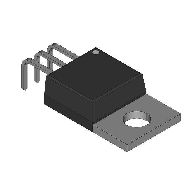
KTP (PowerFLEXE/TO-252*) PACKAGE
(TOP VIEW)
OUTPUT
HEAT
SINK
GND
GND
INPUT
GND
OUTPUT
*Complies with JEDEC TO-252, variation AC
HEAT
SINK
HEAT SINK − These terminals have an internal resistive connection
to ground and should be grounded or electrically isolated.
KCS (TO-220) PACKAGE
(TOP VIEW)
KC (TO-220) PACKAGE
(TOP VIEW)
GND
OUTPUT
GND
INPUT
GND
OUTPUT
GND
INPUT
description/ordering information
ORDERING INFORMATION
TJ
VO
(NOM)
1.8 V
0°C
0
C to 125
125°C
C
TOP-SIDE
MARKING
PowerFLEX/TO-252* (KTP)
Reel of 3000
TLV2217-18KTPR
2217−18
TO-220 (KCS)
Tube of 50
TLV2217-18KCS
TLV2217−18
TO-220 (KC)
Tube of 50
TLV2217-25KC
TLV2217−25
PowerFLEX/TO-252* (KTP)
Reel of 3000
TLV2217-25KTPR
2217−25
Tube of 70
TLV2217-25PW
Reel of 2000
TLV2217-25PWR
PowerFLEX/TO-252* (KTP)
Reel of 3000
TLV2217-33KTPR
2217−33
TO-220 (KC)
Tube of 50
TLV2217-33KC
TLV2217−33
TSSOP (PW)
Reel of 2000
TLV2217-33PWR
2217−33
2.5 V
TSSOP (PW)
3.3 V
ORDERABLE
PART NUMBER
PACKAGE†
2217−25
*Complies to TO-252, variation AC.
† Package drawings, standard packing quantities, thermal data, symbolization, and PCB design guidelines are available at
www.ti.com/sc/package.
Please be aware that an important notice concerning availability, standard warranty, and use in critical applications of
Texas Instruments semiconductor products and disclaimers thereto appears at the end of this data sheet.
PowerFLEX is a trademark of Texas Instruments.
Copyright 2005, Texas Instruments Incorporated
���
�����
��� ����������� �! "#��$�� �! �� %#&'�"����� (��$)
���(#"�! "������ �� !%$"���"�����! %$� �*$ �$��! �� �$+�! ��!��#�$��!
!���(��( ,������-) ���(#"���� %��"$!!��. (�$! ��� �$"$!!���'- ��"'#($
�$!���. �� �'' %����$�$�!)
POST OFFICE BOX 655303
• DALLAS, TEXAS 75265
1
��������
���
����
� ����
������� ���
������
�
�
SLVS067L − MARCH 1992 − REVISED APRIL 2005
description/ordering information (continued)
The TLV2217 family of low-dropout regulators offers a variety of fixed-voltage options that offer a maximum
continuous input voltage of 16 V, making them more versatile than CMOS regulators. Utilizing a pnp pass
element, these regulators are capable of sourcing 500 mA of current, with a specified maximum dropout of
500 mV (3.3-V and 2.5-V options), making these regulators ideal for low-voltage applications. Additionally, the
TLV2217 regulators offer very tight output accuracy of ±2% across operating load and temperature ranges.
Other convenient features the regulators provide are internal overcurrent limiting, thermal-overload protection,
and overvoltage protection. The TLV2217 family of regulators is available in fixed voltages of 1.8 V, 2.5 V, and
3.3 V.
absolute maximum ratings over operating virtual junction temperature range (unless otherwise
noted)†
Continuous input voltage, VI . . . . . . . . . . . . . . . . . . . . . . . . . . . . . . . . . . . . . . . . . . . . . . . . . . . . . . . . . . . . . . . . . 16 V
Operating virtual junction temperature, TJ . . . . . . . . . . . . . . . . . . . . . . . . . . . . . . . . . . . . . . . . . . . . . . . . . . . 150°C
Storage temperature range, Tstg . . . . . . . . . . . . . . . . . . . . . . . . . . . . . . . . . . . . . . . . . . . . . . . . . . . −65°C to 150°C
† Stresses beyond those listed under “absolute maximum ratings” may cause permanent damage to the device. These are stress ratings only, and
functional operation of the device at these or any other conditions beyond those indicated under “recommended operating conditions” is not
implied. Exposure to absolute-maximum-rated conditions for extended periods may affect device reliability.
package thermal data (see Note 1)
PowerFLEX/TO-252 (KTP)
High K, JESD 51-5
θJP‡
1.4°C/W
TO-220 (KC/KCS)
High K, JESD 51-5
3°C/W
PACKAGE
BOARD
θJC
19°C/W
θJA
28°C/W
17°C/W
19°C/W
TSSOP (PW)
High K, JESD 51-7
32°C/W
83°C/W
‡ For packages with exposed thermal pads, such as QFN, PowerPAD, and PowerFLEX, θJP is defined as the thermal resistance between the die
junction and the bottom of the exposed pad.
NOTE 1: Maximum power dissipation is a function of TJ(max), θJA, and TA. The maximum allowable power dissipation at any allowable ambient
temperature is PD = (TJ(max) − TA)/θJA. Operating at the absolute maximum TJ of 150°C can affect reliability.
recommended operating conditions
VI
IO
Input voltage
Output current
TJ
Operating virtual junction temperature range
§ Minimum VI is equal to 3.0 V or VO(max) + 0.6 V, whichever is greater.
2
POST OFFICE BOX 655303
• DALLAS, TEXAS 75265
MIN
MAX
3.0
12
UNIT
V
0
500
mA
0
125
°C
��������
���
����
� ����
������� ���
������
�
SLVS067L − MARCH 1992 − REVISED APRIL 2005
electrical characteristics at VI = 4.5 V, IO = 500 mA, TJ = 25°C (unless otherwise noted)
TLV2217-33
TEST CONDITIONS†
PARAMETER
Output voltage
IO = 20 mA to 500 mA,
VI = 3.8 V to 5.5 V
TJ = 25°C
TJ = 0°C to 125°C
Input voltage regulation
VI = 3.8 V to 5.5 V
f = 120 Hz,
Vripple = 1 VPP
VI = 4.5 V
Ripple rejection
Output voltage regulation
Output noise voltage
MIN
TYP
MAX
3.267
3.30
3.333
3.234
5
Dropout voltage
Bias current
IO = 0
IO = 500 mA
V
15
mV
30
mV
−62
IO = 20 mA to 500 mA
f = 10 Hz to 100 kHz
IO = 250 mA
IO = 500 mA
3.366
UNIT
dB
5
µV
500
400
500
2
5
19
49
mV
mA
† Pulse-testing techniques are used to maintain the virtual junction temperature as close to the ambient temperature as possible. Thermal effects
must be taken into account separately. All characteristics are measured with a 0.1-µF capacitor across the input and a 22-µF tantalum capacitor,
with equivalent series resistance of 1.5 Ω, on the output.
electrical characteristics at VI = 3.3 V, IO = 500 mA, TJ = 25°C (unless otherwise noted)
Output voltage
IO = 20 mA to 500 mA,
Input voltage regulation
VI = 3.0 V to 5.5 V
f = 120 Hz,
Ripple rejection
Output voltage regulation
Output noise voltage
TLV2217-25
TEST CONDITIONS†
PARAMETER
VI = 3.0 V to 5.5 V
TJ = 25°C
TJ = 0°C to 125°C
IO = 250 mA
IO = 500 mA
Bias current
IO = 0
IO = 500 mA
TYP
MAX
2.475
2.5
2.525
2.45
2.55
4
Vripple = 1 VPP,
VI = 4.5 V
IO = 20 mA to 500 mA
f = 10 Hz to 100 kHz
Dropout voltage
MIN
V
12
mV
23
mV
−62
4
UNIT
dB
µV
500
400
500
2
5
19
49
mV
mA
† Pulse-testing techniques are used to maintain the virtual junction temperature as close to the ambient temperature as possible. Thermal effects
must be taken into account separately. All characteristics are measured with a 0.1-µF capacitor across the input and a 22-µF tantalum capacitor,
with equivalent series resistance of 1.5 Ω, on the output.
POST OFFICE BOX 655303
• DALLAS, TEXAS 75265
3
��������
���
����
� ����
������� ���
������
�
�
SLVS067L − MARCH 1992 − REVISED APRIL 2005
electrical characteristics at VI = 3.3 V, IO = 500 mA, TJ = 25°C (unless otherwise noted)
TLV2217-18
TEST CONDITIONS†
PARAMETER
Output voltage
IO = 20 mA to 500 mA,
VI = 3.0 V to 5.5 V
TJ = 25°C
TJ = 0°C to 125°C
Input voltage regulation
VI = 3.0 V to 5.5 V
f = 120 Hz,
Vripple = 1 VPP,
VI = 4.5 V
Ripple rejection
Output voltage regulation
Output noise voltage
Dropout voltage
Bias current
IO = 0
IO = 500 mA
TYP
MAX
1.782
1.8
1.818
1.764
1.836
3
IO = 20 mA to 500 mA
f = 10 Hz to 100 kHz
IO = 250 mA
IO = 500 mA
MIN
V
9
mV
17
mV
−62
3
UNIT
dB
500
‡
µV
‡
mV
2
5
19
49
mA
† Pulse-testing techniques are used to maintain the virtual junction temperature as close to the ambient temperature as possible. Thermal effects
must be taken into account separately. All characteristics are measured with a 0.1-µF capacitor across the input and a 22-µF tantalum capacitor,
with equivalent series resistance of 1.5 Ω, on the output.
‡ Dropout voltage is limited by the input voltage range, with minimum VI = 3.0 V.
4
POST OFFICE BOX 655303
• DALLAS, TEXAS 75265
��������
���
����
� ����
������� ���
������
�
SLVS067L − MARCH 1992 − REVISED APRIL 2005
COMPENSATION-CAPACITOR SELECTION INFORMATION
The TLV2217 is a low-dropout regulator. This means that the capacitance loading is important to the performance
of the regulator because it is a vital part of the control loop. The capacitor value and the equivalent series resistance
(ESR) both affect the control loop and must be defined for the load range and the temperature range. Figures 1 and 2
can be used to establish the capacitance value and ESR range for the best regulator performance.
TLV2217
ESR OF OUTPUT CAPACITOR
vs
LOAD CURRENT
ÇÇÇ
ÇÇÇ
CL = 22 µF
CI = 0.1 µF
TJ = 25°C
2.8
2.6
2.4
Not Recommended
Potential Instability
2.2
2
1.8
1.6
1.4
1.2
1
0.8
0.6
0.4
0.2
0
0.03
0.3
0.4
400 µF
0.02
200 µF
0.015
Minimum
ESR Boundary
0.2
Region of
Best Stability
0.025
ÇÇÇÇÇÇÇÇÇÇÇÇ
ÇÇÇÇÇÇÇÇÇÇÇÇ
ÇÇÇÇÇÇÇÇÇÇÇÇ
ÇÇÇÇÇÇÇÇÇÇÇÇ
ÇÇÇÇÇÇÇÇÇÇÇÇ
ÇÇÇÇÇÇÇÇÇÇÇÇ
ÇÇÇÇÇÇÇÇÇÇÇÇ
0.1
Not Recommended
Potential Instability
Recommended Minimum ESR
1000 µF
0.035
Maximum
ESR Boundary
0
ÇÇÇ
ÇÇÇÇÇÇÇÇÇÇÇÇ
ÇÇÇÇÇÇÇÇÇÇÇÇ
ÇÇÇÇÇÇÇÇÇÇÇÇ
ÇÇÇÇÇÇÇÇÇÇÇÇ
ÇÇÇÇÇÇÇÇÇÇÇÇ
ÇÇÇÇÇÇÇÇÇÇÇÇ
ÇÇÇÇÇÇÇÇÇÇÇÇ
ÇÇÇÇÇÇÇÇÇÇÇÇ
ÇÇÇÇÇÇÇÇÇÇÇÇ
0.04
CL
ESR − Equivalent Series Resistance − Ω
3
TLV2217
STABILITY
vs
ESR
100 mF
0.01
0.005
0
0.5
22 µF
10 µF
0
0.5
1
1.5
Load
Voltage
2.5
3
3.5
4
4.5
5
1/ESR
IL − Load Current − A
Applied Load
Current
2
Figure 2
∆IL
∆VL
∆VL = ESR × ∆IL
Figure 1
typical application schematic
TLV2217-33
INPUT
OUTPUT
VO = 3.3 V
GND
3.8 V
0.1 µF
22 µF
Figure 3
POST OFFICE BOX 655303
• DALLAS, TEXAS 75265
5
�PACKAGE OPTION ADDENDUM
www.ti.com
23-Aug-2010
PACKAGING INFORMATION
Orderable Device
Status
(1)
Package Type Package
Drawing
Pins
Package Qty
Eco Plan
(2)
Lead/
Ball Finish
MSL Peak Temp
(3)
Samples
(Requires Login)
TLV2217-18KCS
ACTIVE
TO-220
KCS
3
50
Pb-Free (RoHS)
CU SN
N / A for Pkg Type
Request Free Samples
TLV2217-18KCSE3
ACTIVE
TO-220
KCS
3
50
Pb-Free (RoHS)
CU SN
N / A for Pkg Type
Request Free Samples
Samples Not Available
TLV2217-18KTPR
OBSOLETE
PFM
KTP
2
TBD
Call TI
Call TI
TLV2217-18KTPRG3
OBSOLETE
PFM
KTP
2
TBD
Call TI
Call TI
Samples Not Available
TLV2217-18KVURG3
ACTIVE
PFM
KVU
3
Green (RoHS
& no Sb/Br)
CU SN
Level-3-260C-168 HR
Request Free Samples
TLV2217-25KC
OBSOLETE
TO-220
KC
3
TBD
Call TI
Call TI
Samples Not Available
TLV2217-25KCE3
OBSOLETE
TO-220
KC
3
TLV2217-25KCSE3
ACTIVE
TO-220
KCS
3
TLV2217-25KTPR
OBSOLETE
PFM
KTP
2
TLV2217-25KTPRG3
OBSOLETE
PFM
KTP
2
TLV2217-25KVURG3
ACTIVE
PFM
KVU
3
2500
50
1
TBD
Call TI
Call TI
Samples Not Available
Pb-Free (RoHS)
CU SN
N / A for Pkg Type
Request Free Samples
TBD
Call TI
Call TI
Samples Not Available
TBD
Call TI
Call TI
Samples Not Available
Green (RoHS
& no Sb/Br)
CU SN
Level-3-260C-168 HR
Request Free Samples
TLV2217-25PW
ACTIVE
TSSOP
PW
20
TBD
Call TI
Call TI
Purchase Samples
TLV2217-25PWE4
ACTIVE
TSSOP
PW
20
TBD
Call TI
Call TI
Purchase Samples
TLV2217-25PWG4
ACTIVE
TSSOP
PW
20
TBD
Call TI
Call TI
TLV2217-25PWR
ACTIVE
TSSOP
PW
20
2000
Green (RoHS
& no Sb/Br)
CU NIPD
Level-1-260C-UNLIM
Contact TI Distributor
or Sales Office
TLV2217-25PWRE4
ACTIVE
TSSOP
PW
20
2000
Green (RoHS
& no Sb/Br)
CU NIPD
Level-1-260C-UNLIM
Contact TI Distributor
or Sales Office
TLV2217-25PWRG4
ACTIVE
TSSOP
PW
20
2000
Green (RoHS
& no Sb/Br)
CU NIPD
Level-1-260C-UNLIM
Contact TI Distributor
or Sales Office
TLV2217-33KC
OBSOLETE
TO-220
KC
3
TBD
Call TI
Call TI
Samples Not Available
TLV2217-33KCE3
OBSOLETE
TO-220
KC
3
TBD
Call TI
Call TI
Samples Not Available
TLV2217-33KCSE3
ACTIVE
TO-220
KCS
3
Pb-Free (RoHS)
CU SN
N / A for Pkg Type
Request Free Samples
TLV2217-33KTPR
OBSOLETE
PFM
KTP
2
TBD
Call TI
Call TI
Samples Not Available
TLV2217-33KTPRG3
OBSOLETE
PFM
KTP
2
TBD
Call TI
Call TI
Samples Not Available
TLV2217-33KVURG3
ACTIVE
PFM
KVU
3
2500
Green (RoHS
& no Sb/Br)
CU SN
Level-3-260C-168 HR
Request Free Samples
TLV2217-33PWR
ACTIVE
TSSOP
PW
20
2000
Green (RoHS
& no Sb/Br)
Call TI
Level-1-260C-UNLIM
Contact TI Distributor
or Sales Office
50
Addendum-Page 1
Purchase Samples
�PACKAGE OPTION ADDENDUM
www.ti.com
Orderable Device
23-Aug-2010
Status
(1)
Package Type Package
Drawing
Pins
Package Qty
Eco Plan
(2)
Lead/
Ball Finish
MSL Peak Temp
(3)
Samples
(Requires Login)
TLV2217-33PWRE4
ACTIVE
TSSOP
PW
20
2000
Green (RoHS
& no Sb/Br)
Call TI
Level-1-260C-UNLIM
Contact TI Distributor
or Sales Office
TLV2217-33PWRG4
ACTIVE
TSSOP
PW
20
2000
Green (RoHS
& no Sb/Br)
Call TI
Level-1-260C-UNLIM
Contact TI Distributor
or Sales Office
(1)
The marketing status values are defined as follows:
ACTIVE: Product device recommended for new designs.
LIFEBUY: TI has announced that the device will be discontinued, and a lifetime-buy period is in effect.
NRND: Not recommended for new designs. Device is in production to support existing customers, but TI does not recommend using this part in a new design.
PREVIEW: Device has been announced but is not in production. Samples may or may not be available.
OBSOLETE: TI has discontinued the production of the device.
(2)
Eco Plan - The planned eco-friendly classification: Pb-Free (RoHS), Pb-Free (RoHS Exempt), or Green (RoHS & no Sb/Br) - please check http://www.ti.com/productcontent for the latest availability
information and additional product content details.
TBD: The Pb-Free/Green conversion plan has not been defined.
Pb-Free (RoHS): TI's terms "Lead-Free" or "Pb-Free" mean semiconductor products that are compatible with the current RoHS requirements for all 6 substances, including the requirement that
lead not exceed 0.1% by weight in homogeneous materials. Where designed to be soldered at high temperatures, TI Pb-Free products are suitable for use in specified lead-free processes.
Pb-Free (RoHS Exempt): This component has a RoHS exemption for either 1) lead-based flip-chip solder bumps used between the die and package, or 2) lead-based die adhesive used between
the die and leadframe. The component is otherwise considered Pb-Free (RoHS compatible) as defined above.
Green (RoHS & no Sb/Br): TI defines "Green" to mean Pb-Free (RoHS compatible), and free of Bromine (Br) and Antimony (Sb) based flame retardants (Br or Sb do not exceed 0.1% by weight
in homogeneous material)
(3)
MSL, Peak Temp. -- The Moisture Sensitivity Level rating according to the JEDEC industry standard classifications, and peak solder temperature.
Important Information and Disclaimer:The information provided on this page represents TI's knowledge and belief as of the date that it is provided. TI bases its knowledge and belief on information
provided by third parties, and makes no representation or warranty as to the accuracy of such information. Efforts are underway to better integrate information from third parties. TI has taken and
continues to take reasonable steps to provide representative and accurate information but may not have conducted destructive testing or chemical analysis on incoming materials and chemicals.
TI and TI suppliers consider certain information to be proprietary, and thus CAS numbers and other limited information may not be available for release.
In no event shall TI's liability arising out of such information exceed the total purchase price of the TI part(s) at issue in this document sold by TI to Customer on an annual basis.
Addendum-Page 2
�PACKAGE MATERIALS INFORMATION
www.ti.com
21-Jul-2010
TAPE AND REEL INFORMATION
*All dimensions are nominal
Device
TLV2217-18KVURG3
Package Package Pins
Type Drawing
PFM
KVU
TLV2217-25KVURG3
PFM
KVU
TLV2217-25PWR
TSSOP
PW
TLV2217-33KVURG3
PFM
KVU
TLV2217-33PWR
TSSOP
PW
3
SPQ
Reel
Reel
A0
Diameter Width (mm)
(mm) W1 (mm)
B0
(mm)
K0
(mm)
P1
(mm)
W
Pin1
(mm) Quadrant
6.9
10.5
2.7
8.0
16.0
Q2
2500
330.0
16.4
3
1
330.0
16.4
6.9
10.5
2.7
8.0
16.0
Q2
20
2000
330.0
16.4
6.95
7.1
1.6
8.0
16.0
Q1
3
2500
330.0
16.4
6.9
10.5
2.7
8.0
16.0
Q2
20
2000
330.0
16.4
6.95
7.1
1.6
8.0
16.0
Q1
Pack Materials-Page 1
�PACKAGE MATERIALS INFORMATION
www.ti.com
21-Jul-2010
*All dimensions are nominal
Device
Package Type
Package Drawing
Pins
SPQ
Length (mm)
Width (mm)
Height (mm)
TLV2217-18KVURG3
PFM
KVU
3
2500
340.0
340.0
38.0
TLV2217-25KVURG3
PFM
KVU
3
1
340.0
340.0
38.0
TLV2217-25PWR
TSSOP
PW
20
2000
346.0
346.0
33.0
TLV2217-33KVURG3
PFM
KVU
3
2500
340.0
340.0
38.0
TLV2217-33PWR
TSSOP
PW
20
2000
346.0
346.0
33.0
Pack Materials-Page 2
�MECHANICAL DATA
MPSF001F – JANUARY 1996 – REVISED JANUARY 2002
KTP (R-PSFM-G2)
PowerFLEX PLASTIC FLANGE-MOUNT PACKAGE
0.080 (2,03)
0.070 (1,78)
0.243 (6,17)
0.233 (5,91)
0.228 (5,79)
0.218 (5,54)
0.050 (1,27)
0.040 (1,02)
0.010 (0,25) NOM
0.130 (3,30) NOM
0.215 (5,46)
NOM
0.247 (6,27)
0.237 (6,02)
Thermal Tab
(See Note C)
0.287 (7,29)
0.277 (7,03)
0.381 (9,68)
0.371 (9,42)
0.100 (2,54)
0.090 (2,29)
0.032 (0,81) MAX
Seating Plane
0.090 (2,29)
0.180 (4,57)
0.004 (0,10)
0.005 (0,13)
0.001 (0,02)
0.031 (0,79)
0.025 (0,63)
0.010 (0,25) M
0.010 (0,25) NOM
Gage Plane
0.047 (1,19)
0.037 (0,94)
0.010 (0,25)
2°–ā6°
4073388/M 01/02
NOTES: A.
B.
C.
D.
E.
All linear dimensions are in inches (millimeters).
This drawing is subject to change without notice.
The center lead is in electrical contact with the thermal tab.
Dimensions do not include mold protrusions, not to exceed 0.006 (0,15).
Falls within JEDEC TO-252 variation AC.
PowerFLEX is a trademark of Texas Instruments.
POST OFFICE BOX 655303
• DALLAS, TEXAS 75265
1
����MECHANICAL DATA
MTSS001C – JANUARY 1995 – REVISED FEBRUARY 1999
PW (R-PDSO-G**)
PLASTIC SMALL-OUTLINE PACKAGE
14 PINS SHOWN
0,30
0,19
0,65
14
0,10 M
8
0,15 NOM
4,50
4,30
6,60
6,20
Gage Plane
0,25
1
7
0°– 8°
A
0,75
0,50
Seating Plane
0,15
0,05
1,20 MAX
PINS **
0,10
8
14
16
20
24
28
A MAX
3,10
5,10
5,10
6,60
7,90
9,80
A MIN
2,90
4,90
4,90
6,40
7,70
9,60
DIM
4040064/F 01/97
NOTES: A.
B.
C.
D.
All linear dimensions are in millimeters.
This drawing is subject to change without notice.
Body dimensions do not include mold flash or protrusion not to exceed 0,15.
Falls within JEDEC MO-153
POST OFFICE BOX 655303
• DALLAS, TEXAS 75265
�IMPORTANT NOTICE
Texas Instruments Incorporated and its subsidiaries (TI) reserve the right to make corrections, modifications, enhancements, improvements,
and other changes to its products and services at any time and to discontinue any product or service without notice. Customers should
obtain the latest relevant information before placing orders and should verify that such information is current and complete. All products are
sold subject to TI’s terms and conditions of sale supplied at the time of order acknowledgment.
TI warrants performance of its hardware products to the specifications applicable at the time of sale in accordance with TI’s standard
warranty. Testing and other quality control techniques are used to the extent TI deems necessary to support this warranty. Except where
mandated by government requirements, testing of all parameters of each product is not necessarily performed.
TI assumes no liability for applications assistance or customer product design. Customers are responsible for their products and
applications using TI components. To minimize the risks associated with customer products and applications, customers should provide
adequate design and operating safeguards.
TI does not warrant or represent that any license, either express or implied, is granted under any TI patent right, copyright, mask work right,
or other TI intellectual property right relating to any combination, machine, or process in which TI products or services are used. Information
published by TI regarding third-party products or services does not constitute a license from TI to use such products or services or a
warranty or endorsement thereof. Use of such information may require a license from a third party under the patents or other intellectual
property of the third party, or a license from TI under the patents or other intellectual property of TI.
Reproduction of TI information in TI data books or data sheets is permissible only if reproduction is without alteration and is accompanied
by all associated warranties, conditions, limitations, and notices. Reproduction of this information with alteration is an unfair and deceptive
business practice. TI is not responsible or liable for such altered documentation. Information of third parties may be subject to additional
restrictions.
Resale of TI products or services with statements different from or beyond the parameters stated by TI for that product or service voids all
express and any implied warranties for the associated TI product or service and is an unfair and deceptive business practice. TI is not
responsible or liable for any such statements.
TI products are not authorized for use in safety-critical applications (such as life support) where a failure of the TI product would reasonably
be expected to cause severe personal injury or death, unless officers of the parties have executed an agreement specifically governing
such use. Buyers represent that they have all necessary expertise in the safety and regulatory ramifications of their applications, and
acknowledge and agree that they are solely responsible for all legal, regulatory and safety-related requirements concerning their products
and any use of TI products in such safety-critical applications, notwithstanding any applications-related information or support that may be
provided by TI. Further, Buyers must fully indemnify TI and its representatives against any damages arising out of the use of TI products in
such safety-critical applications.
TI products are neither designed nor intended for use in military/aerospace applications or environments unless the TI products are
specifically designated by TI as military-grade or "enhanced plastic." Only products designated by TI as military-grade meet military
specifications. Buyers acknowledge and agree that any such use of TI products which TI has not designated as military-grade is solely at
the Buyer's risk, and that they are solely responsible for compliance with all legal and regulatory requirements in connection with such use.
TI products are neither designed nor intended for use in automotive applications or environments unless the specific TI products are
designated by TI as compliant with ISO/TS 16949 requirements. Buyers acknowledge and agree that, if they use any non-designated
products in automotive applications, TI will not be responsible for any failure to meet such requirements.
Following are URLs where you can obtain information on other Texas Instruments products and application solutions:
Products
Applications
Amplifiers
amplifier.ti.com
Audio
www.ti.com/audio
Data Converters
dataconverter.ti.com
Automotive
www.ti.com/automotive
DLP® Products
www.dlp.com
Communications and
Telecom
www.ti.com/communications
DSP
dsp.ti.com
Computers and
Peripherals
www.ti.com/computers
Clocks and Timers
www.ti.com/clocks
Consumer Electronics
www.ti.com/consumer-apps
Interface
interface.ti.com
Energy
www.ti.com/energy
Logic
logic.ti.com
Industrial
www.ti.com/industrial
Power Mgmt
power.ti.com
Medical
www.ti.com/medical
Microcontrollers
microcontroller.ti.com
Security
www.ti.com/security
RFID
www.ti-rfid.com
Space, Avionics &
Defense
www.ti.com/space-avionics-defense
RF/IF and ZigBee® Solutions www.ti.com/lprf
Video and Imaging
www.ti.com/video
Wireless
www.ti.com/wireless-apps
Mailing Address: Texas Instruments, Post Office Box 655303, Dallas, Texas 75265
Copyright © 2010, Texas Instruments Incorporated
�


 工商网监
湘ICP备2023018690号
工商网监
湘ICP备2023018690号
