Order
Now
Product
Folder
Support &
Community
Tools &
Software
Technical
Documents
TLV62568A, TLV62569A
ZHCSI23B – APRIL 2018 – REVISED MARCH 2020
采用 SOT563 封装并具有强制 PWM 的 TLV6256xA 1A、
、2A 降压转换器
1 特性
•
•
•
•
•
•
•
•
•
•
•
•
•
•
1
3 说明
强制 PWM 模式可减少输出电压纹波
效率高达 95%
低 RDS(ON) 开关:100mΩ/60mΩ
输入电压范围为 2.5V 至 5.5V
可调输出电压范围为 0.6V 至 VIN
100% 占空比,可实现超低压降
1.5MHz 典型开关频率
电源正常输出
过流保护
内部软启动
热关断保护
采用 SOT563 封装
与 TLV62568、TLV62569 引脚对引脚兼容
借助 WEBENCH® 电源设计器创建定制设计方案
2 应用
•
•
•
•
•
TLV62568A、TLV62569A 器件是经过优化而具有高效
率和紧凑型解决方案尺寸的同步降压型直流/直流转换
器。该器件集成了输出电流高达 2A 的开关。在整个负
载范围内,该器件将以 1.5MHz 开关频率在脉宽调制
(PWM) 模式下运行。关断时,流耗减少至 2μA 以下。
内部软启动电路可限制启动期间的浪涌电流。此外,
还内置了 诸如输出过流保护、热关断保护和电源正常
输出等其他特性。该器件采用 SOT563 封装。
器件信息(1)
器件型号
封装
TLV62568APDRL
TLV62569ADRL
SOT563 (6)
TLV62569APDRL
器件比较
器件型号
输出电流
TLV62568ADRL
100
VOUT
1.8 V / 2.0 A
L1
1.0 µH
SW
95
C2
22 µF
EN
C3*
90
R1
200 k
GND FB
C3: Optional
电源正常
sp
sp在
在 5V 输入电压下的效率
R2
100 k
Efficiency (%)
VIN
C1
4.7 µF
电源正常
2A
TLV62569APDRL
sp
sp
sp典
典型应用原理图
功能
1A
TLV62568APDRL
TLV62569ADRL
TLV62569A
1.60mm x 1.60mm
(1) 如需了解所有可用封装,请参阅产品说明书末尾的可订购产品
附录。
通用负载点 (POL) 电源
STB 和 DVR
IP 网络摄像头
无线路由器
固态硬盘 (SSD) – 企业级
VIN
2.5 V to 5.5 V
封装尺寸(标称值)
TLV62568ADRL
85
80
75
70
VOUT
VOUT
VOUT
VOUT
Copyright Ú 2016, Texas Instruments Incorporated
65
60
0.0
0.5
1.0
Load (A)
1.5
=
=
=
=
1.2
1.8
2.5
3.3
V
V
V
V
2.0
D008
1
本文档旨在为方便起见,提供有关 TI 产品中文版本的信息,以确认产品的概要。 有关适用的官方英文版本的最新信息,请访问 www.ti.com,其内容始终优先。 TI 不保证翻译的准确
性和有效性。 在实际设计之前,请务必参考最新版本的英文版本。
English Data Sheet: SLVSE95
�TLV62568A, TLV62569A
ZHCSI23B – APRIL 2018 – REVISED MARCH 2020
www.ti.com.cn
目录
1
2
3
4
5
6
7
特性 ..........................................................................
应用 ..........................................................................
说明 ..........................................................................
修订历史记录 ...........................................................
Pin Configuration and Functions .........................
Specifications.........................................................
1
1
1
2
3
3
6.1
6.2
6.3
6.4
6.5
6.6
3
3
4
4
4
5
Absolute Maximum Ratings ......................................
ESD Ratings..............................................................
Recommended Operating Conditions.......................
Thermal Information ..................................................
Electrical Characteristics...........................................
Typical Characteristics ..............................................
Detailed Description .............................................. 6
7.1
7.2
7.3
7.4
Overview ...................................................................
Functional Block Diagrams .......................................
Feature Description...................................................
Device Functional Modes..........................................
6
6
6
7
8
Application and Implementation .......................... 8
8.1 Application Information.............................................. 8
8.2 Typical Application .................................................... 8
9 Power Supply Recommendations...................... 13
10 Layout................................................................... 13
10.1 Layout Guidelines ................................................. 13
10.2 Layout Example .................................................... 13
10.3 Thermal Considerations ........................................ 14
11 器件和文档支持 ..................................................... 14
11.1
11.2
11.3
11.4
11.5
11.6
11.7
器件支持 ...............................................................
文档支持 ...............................................................
接收文档更新通知 .................................................
支持资源................................................................
商标 .......................................................................
静电放电警告.........................................................
Glossary ................................................................
14
14
14
14
15
15
15
12 机械、封装和可订购信息 ....................................... 15
4 修订历史记录
Changes from Revision A (May 2018) to Revision B
•
Page
已更改 Power Good pin sink current capability from 1 mA to 2 mA ...................................................................................... 7
Changes from Original (April 2018) to Revision A
Page
•
已更改 将状态从“预告信息”更改为“生产数据” ........................................................................................................................ 1
2
Copyright © 2018–2020, Texas Instruments Incorporated
�TLV62568A, TLV62569A
www.ti.com.cn
ZHCSI23B – APRIL 2018 – REVISED MARCH 2020
5 Pin Configuration and Functions
SOT563-6
DRL Package
(Top View)
NC/PG EN
SW
6
5
4
1
2
3
FB GND VIN
Pin Functions
SOT563-6
NAME
PIN
NUMBER
I/O/PWR
DESCRIPTION
FB
1
I
GND
2
PWR
Ground pin.
VIN
3
PWR
Power supply voltage input.
SW
4
PWR
Switch pin connected to the internal FET switches and inductor terminal. Connect the inductor of
the output filter to this pin.
EN
5
I
Device enable logic input. Logic high enables the device, logic low disables the device and turns
it into shutdown. Do not leave floating.
PG
6
O
Power good open drain output pin for TLV62569APDRL. The pull-up resistor should not be
connected to any voltage higher than 5.5V. If it's not used, leave the pin floating.
NC
6
-
No connection pin for TLV62569ADRL. The pin can be connected to the output or the ground for
enhancing thermal performance. Or leave it floating.
Feedback pin for the internal control loop. Connect this pin to an external feedback divider.
6 Specifications
6.1 Absolute Maximum Ratings
over operating temperature range (unless otherwise noted) (1)
VIN, EN, PG
Voltage (2)
SW (DC)
SW (AC, less than 10ns)
(3)
MIN
MAX
-0.3
6
UNIT
-0.3
VIN + 0.3
-3.0
9
V
FB
-0.3
3
TJ
Junction temperature
-40
150
°C
Tstg
Storage temperature
-65
150
°C
(1)
(2)
(3)
Stresses beyond those listed under Absolute Maximum Rating may cause permanent damage to the device. These are stress ratings
only, which do not imply functional operation of the device at these or any other conditions beyond those indicated under Recommended
Operating Condition. Exposure to absolute-maximum-rated conditions for extended periods may affect device reliability.
All voltage values are with respect to network ground terminal.
While switching.
6.2 ESD Ratings
VALUE
V(ESD)
(1)
(2)
Electrostatic discharge
Human body model (HBM), per
ANSI/ESDA/JEDEC JS-001, all pins (1)
±2000
Charged device model (CDM), per JEDEC
specification JESD22-C101, all pins (2)
±500
UNIT
V
JEDEC document JEP155 states that 500-V HBM allows safe manufacturing with a standard ESD control process.
JEDEC document JEP157 states that 250-V CDM allows safe manufacturing with a standard ESD control process.
Copyright © 2018–2020, Texas Instruments Incorporated
3
�TLV62568A, TLV62569A
ZHCSI23B – APRIL 2018 – REVISED MARCH 2020
www.ti.com.cn
6.3 Recommended Operating Conditions
over operating free-air temperature range (unless otherwise noted)
MIN
NOM
MAX
UNIT
VIN
Input voltage
2.5
5.5
V
VOUT
Output voltage
0.6
VIN
V
IOUT
Output current
0
2
A
TJ
Junction temperature
-40
125
°C
6.4 Thermal Information
TLV62568Ax, TLV62569Ax
THERMAL METRIC
RθJA
(1)
Junction-to-ambient thermal resistance
JEDEC (DRL)
EVM (DRL)
6 PINS
6 PINS
UNIT
142.8
124.8
°C/W
°C/W
°C/W
RθJC(top)
Junction-to-case (top) thermal resistance
51.1
n/a
(2)
RθJB
Junction-to-board thermal resistance
28.9
n/a
(2)
ΨJT
Junction-to-top characterization parameter
1.4
1.6
°C/W
ΨJB
Junction-to-board characterization parameter
28.7
23.1
°C/W
(1)
(2)
For more information about traditional and new thermal metrics, see the Semiconductor and IC Package Thermal Metrics application
report.
Not applicable to an EVM.
6.5 Electrical Characteristics
VIN = 5.0 V, TJ = 25 °C, unless otherwise noted
PARAMETER
TEST CONDITIONS
MIN
TYP
MAX
0.01
2
2.3
2.45
UNIT
SUPPLY
ISD
VUVLO
TJSD
Shutdown current into VIN pin
EN = 0 V
Under voltage lock out
VIN falling
under voltage lock out hysteresis
Thermal shutdown
100
TJ rising
150
TJ falling
130
µA
V
mV
°C
LOGIC INTERFACE
VIH
High-level input voltage at EN pin
2.5 ≤ VIN ≤ 5.5
VIL
Low-level input voltage at EN pin
2.5 ≤ VIN ≤ 5.5
tSS
Soft startup time
From EN high to 95% of VOUT
nominal
VPG
Power good threshold
VPG,OL
Low-level output voltage at PG pin
ISINK = 1 mA
IPG,LKG
Input leakage current into PG pin
VPG = 5 V
100
nA
tPG,DLY
Power good delay time
VFB falling
40
µs
4
1.2
V
0.4
0.9
VFB rising, referenced to VFB nominal
95%
VFB falling, referenced to VFB nominal
90%
V
ms
0.4
V
Copyright © 2018–2020, Texas Instruments Incorporated
�TLV62568A, TLV62569A
www.ti.com.cn
ZHCSI23B – APRIL 2018 – REVISED MARCH 2020
Electrical Characteristics (continued)
VIN = 5.0 V, TJ = 25 °C, unless otherwise noted
PARAMETER
TEST CONDITIONS
MIN
TYP
MAX
0.588
0.6
0.612
UNIT
OUTPUT
VFB
Feedback regulation voltage
IFB
Input leakage current into FB pin
RDS(on)
VFB = 0.6 V
High-side FET on resistance
100
Low-side FET on resistance
60
ILIM
High-side FET current limit
fSW
Switching frequency
V
10
TLV62569A, TLV62569AP
3
TLV62568A, TLV62568AP
2
nA
mΩ
A
1.5
MHz
6.6 Typical Characteristics
0.606
0.5
0.603
FB Voltage (V)
6KXWGRZQ &XUUHQW
$
0.4
VIN = 2.5V
VIN = 3.6V
VIN = 5.0V
0.3
0.2
0.600
0.597
TJ
TJ
TJ
TJ
0.1
0.0
-40
-20
0
20
40
60
80
Junction Temperature (°C)
100
0.594
2.5
120
3.0
3.5
D002
5.0
5.5
D003
Switch Current Limit (A)
3.0
3.5
3.0
2.5
2.0
VIN = 2.7V
VIN = 3.6V
VIN = 5.0V
2.5
-40
-40°C
25°C
85°C
125°C
图 2. FB Voltage Accuracy
图 1. Shutdown Current vs Junction Temperature
4.0
Switch Current Limit (A)
4.0
4.5
Input Voltage (V)
=
=
=
=
-20
0
20
40
60
80
Junction Temperature (°C)
100
图 3. Switch Current Limit, TLV62569A
版权 © 2018–2020, Texas Instruments Incorporated
VIN = 2.7V
VIN = 3.6V
VIN = 5.0V
1.5
-40
120
D020
-20
0
20
40
60
80
Junction Temperature (°C)
100
120
D021
图 4. Switch Current Limit, TLV62568A
5
�TLV62568A, TLV62569A
ZHCSI23B – APRIL 2018 – REVISED MARCH 2020
www.ti.com.cn
7 Detailed Description
7.1 Overview
The device is a high-efficiency synchronous step-down converter. The device operates with an adaptive off time
with peak current control scheme. The device operates at typically 1.5-MHz frequency pulse width modulation
(PWM) . Based on the VIN/VOUT ratio, a simple circuit sets the required off time for the low-side MOSFET. It
makes the switching frequency relatively constant regardless of the variation of input voltage, output voltage, and
load current.
7.2 Functional Block Diagrams
PG
Soft Start
Thermal
Shutdown
UVLO
Control Logic
EN
VPG
+
VFB
±
VIN
GND
Peak Current Detect
VREF
+
_
FB
Modulator
SW
Gate
Drive
VSW
VIN
TOFF
GND
GND
Copyright Ú 2018, Texas Instruments Incorporated
图 5. TLV62569A Functional Block Diagram
7.3 Feature Description
7.3.1 100% Duty Cycle Low Dropout Operation
The device offers a low input-to-output voltage differential by entering 100% duty cycle mode. In this mode, the
high-side MOSFET switch is constantly turned on and the low-side MOSFET is switched off. The minimum input
voltage to maintain output regulation, depending on the load current and output voltage, is calculated as:
VIN(MIN) = VOUT + IOUT x (RDS(ON) + RL)
where
•
•
RDS(ON) = High side FET on-resistance
RL = Inductor ohmic resistance (DCR)
(1)
7.3.2 Soft Startup
After enabling the device, internal soft startup circuitry ramps up the output voltage which reaches nominal output
voltage during a startup time. This avoids excessive inrush current and creates a smooth output voltage rise
slope. It also prevents excessive voltage drops of primary cells and rechargeable batteries with high internal
impedance.
6
版权 © 2018–2020, Texas Instruments Incorporated
�TLV62568A, TLV62569A
www.ti.com.cn
ZHCSI23B – APRIL 2018 – REVISED MARCH 2020
Feature Description (接
接下页)
The device is able to start into a pre-biased output capacitor. The converter starts with the applied bias voltage
and ramps the output voltage to its nominal value.
7.3.3 Switch Current Limit
The switch current limit prevents the device from high inductor current and drawing excessive current from a
battery or input voltage rail. Excessive current might occur with a heavy load or shorted output circuit condition.
The device adopts the peak current control by sensing the current of the high-side switch. Once the high-side
switch current limit is reached, the high-side switch is turned off and low-side switch is turned on to ramp down
the inductor current with an adaptive off-time.
7.3.4 Under Voltage Lockout
To avoid mis-operation of the device at low input voltages, under voltage lockout is implemented that shuts down
the device at voltages lower than VUVLO with VHYS_UVLO hysteresis.
7.3.5 Thermal Shutdown
The device enters thermal shutdown once the junction temperature exceeds the thermal shutdown rising
threshold, TJSD. Once the junction temperature falls below the falling threshold, the device returns to normal
operation automatically.
7.4 Device Functional Modes
7.4.1 Enabling/Disabling the Device
The device is enabled by setting the EN input to a logic High. Accordingly, a logic Low disables the device. If the
device is enabled, the internal power stage starts switching and regulates the output voltage to the set point
voltage. The EN input must be terminated and should not be left floating.
7.4.2 Power Good
The TLV62568AP and TLV62569AP have a power good output. The PG pin goes high impedance once the
output is above 95% of the nominal voltage, and is driven low once the output voltage falls below typically 90%
of the nominal voltage. The PG pin is an open-drain output and is specified to sink up to 2 mA. The power good
output requires a pull-up resistor connecting to any voltage rail less than 5.5 V. The PG signal can be used for
sequencing of multiple rails by connecting it to the EN pin of other converters. Leave the PG pin unconnected
when not used.
表 1. PG Pin Logic
DEVICE CONDITIONS
Enable
EN = High, VFB ≥ VPG
LOGIC STATUS
HIGH Z
LOW
√
EN = High, VFB ≤ VPG
√
Shutdown
EN = Low
√
Thermal Shutdown
TJ > TJSD
√
UVLO
1.4 V < VIN < VUVLO
Power Supply Removal
VIN ≤ 1.4 V
版权 © 2018–2020, Texas Instruments Incorporated
√
√
7
�TLV62568A, TLV62569A
ZHCSI23B – APRIL 2018 – REVISED MARCH 2020
www.ti.com.cn
8 Application and Implementation
注
Information in the following applications sections is not part of the TI component
specification, and TI does not warrant its accuracy or completeness. TI’s customers are
responsible for determining suitability of components for their purposes. Customers should
validate and test their design implementation to confirm system functionality.
8.1 Application Information
The following section discusses the design of the external components to complete the power supply design for
several input and output voltage options by using typical applications as a reference.
8.2 Typical Application
VIN
2.5 V to 5.5 V
TLV62569A
VIN
C1
4.7 µF
VOUT
1.8 V / 2.0 A
L1
1.0 µH
SW
C2
22 µF
EN
C3*
R1
200 k
GND FB
R2
100 k
C3: Optional
Copyright Ú 2016, Texas Instruments Incorporated
图 6. TLV62569A 1.8-V Output Application
8.2.1 Design Requirements
For this design example, use the parameters listed in 表 2 as the input parameters.
表 2. Design Parameters
DESIGN PARAMETER
EXAMPLE VALUE
Input voltage
2.5 V to 5.5 V
Output voltage
1.8 V
Maximum output current
2.0 A
表 3 lists the components used for the example.
表 3. List of Components
REFERENCE
C1
4.7 µF, Ceramic Capacitor, 10 V, X7R, size 0805, GRM21BR71A475KA73L
Murata
C2
22 µF, Ceramic Capacitor, 6.3 V, X7T, size 0805, GRM21BD70J226ME44
Murata
L1
1.0 µH, Power Inductor, size 4mmx4mm, XAL4020-102ME
Coilcraft
R1,R2,R3
C3
(1)
MANUFACTURER (1)
DESCRIPTION
Chip resistor,1%,size 0603
Std.
Optional, 10 pF if it is needed
Std.
See Third-party Products Disclaimer
8.2.2 Detailed Design Procedure
8.2.2.1 Custom Design With WEBENCH® Tools
Click here to create a custom design using the TLV62569A device with the WEBENCH® Power Designer.
8
版权 © 2018–2020, Texas Instruments Incorporated
�TLV62568A, TLV62569A
www.ti.com.cn
ZHCSI23B – APRIL 2018 – REVISED MARCH 2020
1. Start by entering the input voltage (VIN), output voltage (VOUT), and output current (IOUT) requirements.
2. Optimize the design for key parameters such as efficiency, footprint, and cost using the optimizer dial.
3. Compare the generated design with other possible solutions from Texas Instruments.
The WEBENCH Power Designer provides a customized schematic along with a list of materials with real-time
pricing and component availability.
In most cases, these actions are available:
• Run electrical simulations to see important waveforms and circuit performance
• Run thermal simulations to understand board thermal performance
• Export customized schematic and layout into popular CAD formats
• Print PDF reports for the design, and share the design with colleagues
Get more information about WEBENCH tools at www.ti.com/WEBENCH.
8.2.2.2 Setting the Output Voltage
An external resistor divider is used to set output voltage according to 公式 2.
When sizing R2, in order to achieve low current consumption and acceptable noise sensitivity, use a maximum of
200 kΩ for R2. Larger currents through R2 improve noise sensitivity and output voltage accuracy but increase
current consumption.
R1 ö
R1 ö
æ
æ
VOUT = VFB ´ ç 1 +
÷
÷ = 0.6V ´ ç 1 +
R2 ø
R2 ø
è
è
(2)
A feed forward capacitor, C3 improves the loop bandwidth to make a fast transient response (shown in 图 24). A
10-pF capacitance is recommended for R2 of 100-kΩ resistance. A more detailed discussion on the optimization
for stability vs. transient response can be found in SLVA289.
8.2.2.3 Output Filter Design
The inductor and output capacitor together provide a low-pass filter. To simplify this process, 表 4 outlines
possible inductor and capacitor value combinations. Checked cells represent combinations that are proven for
stability by simulation and lab test. Further combinations should be checked for each individual application.
表 4. Matrix of Output Capacitor and Inductor Combinations
(1)
(2)
(3)
VOUT [V]
L [µH] (1)
0.6 ≤ VOUT < 1.2
1
1.2 ≤ VOUT
1
COUT [µF] (2)
4.7
10
22
47
100
+
++ (3)
+
Inductor tolerance and current de-rating is anticipated. The effective inductance can vary by +20% and -30%.
Capacitance tolerance and bias voltage de-rating is anticipated. The effective capacitance can vary by +20% and -50%.
This LC combination is the standard value and recommended for most applications.
8.2.2.4 Inductor Selection
The main parameters for inductor selection is inductor value and then saturation current of the inductor. To
calculate the maximum inductor current under static load conditions, 公式 3 is given:
DI
IL,MAX = IOUT,MAX + L
2
VOUT
VIN
DIL = VOUT ´
L ´ fSW
1-
where:
•
•
IOUT,MAX is the maximum output current
ΔIL is the inductor current ripple
版权 © 2018–2020, Texas Instruments Incorporated
9
�TLV62568A, TLV62569A
ZHCSI23B – APRIL 2018 – REVISED MARCH 2020
•
•
www.ti.com.cn
fSW is the switching frequency
L is the inductor value
(3)
It is recommended to choose a saturation current for the inductor that is approximately 20% to 30% higher than
IL,MAX. In addition, DC resistance and size should also be taken into account when selecting an appropriate
inductor.
8.2.2.5 Input and Output Capacitor Selection
The architecture of the device allows use of tiny ceramic-type output capacitors with low equivalent series
resistance (ESR). These capacitors provide low output voltage ripple and are thus recommended. To keep its
resistance up to high frequencies and to achieve narrow capacitance variation with temperature, it is
recommended to use X7T or X5R dielectric.
The input capacitor is the low impedance energy source for the converter that helps provide stable operation. A
low ESR multilayer ceramic capacitor is recommended for best filtering. For most applications, 4.7-μF input
capacitance is sufficient; a larger value reduces input voltage ripple.
The device is designed to operate with an output capacitor of 22 µF to 47 µF, as outlined in 表 4.
8.2.3 Application Performance Curves
VIN = 5 V, VOUT = 1.8 V, TA = 25 °C, external components shown in 表 3, unless otherwise noted.
95
10
85
Efficiency (%)
Quiescent Current (mA)
90
8
6
4
TJ
TJ
TJ
TJ
2
0
2.5
3.0
3.5
4.0
4.5
Input Voltage (V)
=
=
=
=
5.0
80
75
70
65
-40°C
25°C
85°C
125°C
VIN = 3.3 V
VIN = 4.2 V
VIN = 5.0 V
60
55
0.0
5.5
0.5
D001
1.0
Load (A)
1.5
2.0
D005
VOUT = 0.6 V
图 8. 0.6-V Output Efficiency
100
100
95
95
90
90
Efficiency (%)
Efficiency (%)
图 7. Quiescent Current
85
80
75
70
0.5
1.0
Load (A)
1.5
图 9. 1.2-V Output Efficiency
10
80
75
70
VIN = 3.3 V
VIN = 4.2 V
VIN = 5.0 V
65
60
0.0
85
VIN = 3.3 V
VIN = 4.2 V
VIN = 5.0 V
65
2.0
D006
60
0.0
0.5
1.0
Load (A)
1.5
2.0
D004
图 10. 1.8-V Output Efficiency
版权 © 2018–2020, Texas Instruments Incorporated
�TLV62568A, TLV62569A
ZHCSI23B – APRIL 2018 – REVISED MARCH 2020
100
100
95
95
90
90
Efficiency (%)
Efficiency (%)
www.ti.com.cn
85
80
75
70
85
80
75
70
VIN = 3.3 V
VIN = 4.2 V
VIN = 5.0 V
65
60
0.0
0.5
1.0
Load (A)
1.5
65
VIN = 4.2 V
VIN = 5.0 V
60
0.0
2.0
0.5
1.0
Load (A)
D019
图 11. 2.5-V Output Efficiency
1.5
2.0
D007
图 12. 3.3-V Output Efficiency
1.00
100
95
Load Regulation (%)
Efficiency (%)
90
85
80
75
70
VOUT
VOUT
VOUT
VOUT
65
60
0.0
0.5
1.0
Load (A)
=
=
=
=
1.2
1.8
2.5
3.3
1.5
V
V
V
V
0.50
0.00
-0.50
VOUT
VOUT
VOUT
VOUT
=
=
=
=
-1.00
0.0
2.0
D008
0.6
1.2
1.8
3.3
V
V
V
V
0.5
1.0
Load (A)
1.5
2.0
D009
VIN = 5 V
图 14. Load Regulation
图 13. 5.0-V Input Efficiency
4.0
1.00
Maximum Output Current (A)
Line Regulation (%)
3.5
0.50
0.00
-0.50
-1.00
2.5
VOUT
VOUT
VOUT
VOUT
3.0
3.5
4.0
4.5
Input Voltage (V)
IOUT = 1 A
5.0
=
=
=
=
0.6
1.2
1.8
3.3
V
V
V
V
3.0
2.5
2.0
1.5
1.0
TA = 25°C
TA = 65°C
TA = 85°C
0.5
5.5
0.0
2.5
3.0
D010
3.5
4.0
4.5
Input Voltage (V)
5.0
5.5
D019
PG is high
图 15. Line Regulation
版权 © 2018–2020, Texas Instruments Incorporated
图 16. Maximum Output Current at VOUT = 1.8 V
11
�TLV62568A, TLV62569A
ZHCSI23B – APRIL 2018 – REVISED MARCH 2020
www.ti.com.cn
2000
Switching Frequency (kHz)
Switching Frequency (kHz)
2000
1500
1000
VOUT
VOUT
VOUT
VOUT
VOUT
500
=
=
=
=
=
0.6
1.2
1.8
2.5
3.3
V
V
V
V
V
0
0
0.5
1
Load (A)
1.5
2
1500
1000
VOUT
VOUT
VOUT
VOUT
VOUT
500
0
2.5
3
D011
3.5
4
4.5
Input Voltage (V)
=
=
=
=
=
5
V
V
V
V
V
5.5
D012
IOUT = 1 A
VIN = 5 V
图 18. Switching Frequency vs Input Voltage
图 17. Switching Frequency vs Load
VSW
5V/DIV
VSW
5V/DIV
ICOIL
0.5A/DIV
ICOIL
0.5A/DIV
VOUT
10mV/DIV
AC
VOUT
10mV/DIV
AC
Time - 500ns/DIV
Time - 500ns/DIV
D013
D014
IOUT = 36 mA
IOUT = 1 A
图 19. PWM Operation
图 20. PWM Operation
VEN
2V/DIV
VEN
2V/DIV
VOUT
0.5V/DIV
VOUT
0.5V/DIV
ICOIL
1A/DIV
ICOIL
0.5A/DIV
7LPH
V ',9
7LPH
V ',9
D015
Load = 0.9 Ω
图 21. Startup and Shutdown with Load
12
0.6
1.2
1.8
2.5
3.3
D016
Load = 9 Ω
图 22. Startup and Shutdown with Load
版权 © 2018–2020, Texas Instruments Incorporated
�TLV62568A, TLV62569A
www.ti.com.cn
ZHCSI23B – APRIL 2018 – REVISED MARCH 2020
VOUT
0.1V/DIV
AC
VOUT
0.1V/DIV
AC
ICOIL
0.5A/DIV
ICOIL
0.5A/DIV
7LPH
V ',9
7LPH
V ',9
D017
Load Step 0 A to 1 A, 1A/μs slew rate
D018
Load Step 0 A to 1 A, 1A/μs slew rate
图 23. Load Transient
C3 = 10 pF
图 24. Load Transient with A Feed Forward Capacitor
9 Power Supply Recommendations
The power supply to the TLV62569A must have a current rating according to the supply voltage, output voltage
and output current.
10 Layout
10.1 Layout Guidelines
The PCB layout is an important step to maintain the high performance of the TLV62569A device.
• The input/output capacitors and the inductor should be placed as close as possible to the IC. This keeps the
power traces short. Routing these power traces direct and wide results in low trace resistance and low
parasitic inductance.
• The low side of the input and output capacitors must be connected properly to the power GND to avoid a
GND potential shift.
• The sense traces connected to FB are signal traces. Special care should be taken to avoid noise being
induced. Keep these traces away from SW nodes.
• GND layers might be used for shielding.
10.2 Layout Example
GND
R1
R2
C1
VIN
FB
GND
VIN
L1
PG
EN
SW
C2
VOUT
图 25. TLV62569APDRL Layout
版权 © 2018–2020, Texas Instruments Incorporated
13
�TLV62568A, TLV62569A
ZHCSI23B – APRIL 2018 – REVISED MARCH 2020
www.ti.com.cn
10.3 Thermal Considerations
Implementation of integrated circuits in low-profile and fine-pitch surface-mount packages typically requires
special attention to power dissipation. Many system-dependent issues such as thermal coupling, airflow,
convection surfaces, and the presence of other heat-generating components affect the power dissipation limits of
a given component.
Two basic approaches for enhancing thermal performance are listed below:
• Improving the power dissipation capability of the PCB design
• Introducing airflow in the system
For more details on how to use the thermal parameters, see the application notes: Thermal Characteristics
Application Notes SZZA017 and SPRA953.
11 器件和文档支持
11.1 器件支持
11.1.1 第三方产品免责声明
TI 发布的与第三方产品或服务有关的信息,不能构成与此类产品或服务或保修的适用性有关的认可,不能构成此类
产品或服务单独或与任何 TI 产品或服务一起的表示或认可。
11.1.2 开发支持
11.1.2.1 使用 WEBENCH® 工具创建定制设计
单击此处,使用 TLV62569A 器件并借助 WEBENCH® 电源设计器创建定制设计方案。
1. 首先输入输入电压 (VIN)、输出电压 (VOUT) 和输出电流 (IOUT) 要求。
2. 使用优化器拨盘优化该设计的关键参数,如效率、尺寸和成本。
3. 将生成的设计与德州仪器 (TI) 的其他可行的解决方案进行比较。
WEBENCH 电源设计器可提供定制原理图以及罗列实时价格和组件供货情况的物料清单。
在多数情况下,可执行以下操作:
• 运行电气仿真,观察重要波形以及电路性能
• 运行热性能仿真,了解电路板热性能
• 将定制原理图和布局方案以常用 CAD 格式导出
• 打印设计方案的 PDF 报告并与同事共享
有关 WEBENCH 工具的详细信息,请访问 www.ti.com.cn/WEBENCH。
11.2 文档支持
11.2.1 相关文档
• 德州仪器 (TI),《半导体和 IC 封装热指标》 应用报告
• 德州仪器 (TI),《采用 JEDEC PCB 设计的线性和逻辑封装热工特性》 应用报告
11.3 接收文档更新通知
要接收文档更新通知,请导航至 ti.com.cn 上的器件产品文件夹。单击右上角的通知我进行注册,即可每周接收产
品信息更改摘要。有关更改的详细信息,请查看任何已修订文档中包含的修订历史记录。
11.4 支持资源
TI E2E™ support forums are an engineer's go-to source for fast, verified answers and design help — straight
from the experts. Search existing answers or ask your own question to get the quick design help you need.
Linked content is provided "AS IS" by the respective contributors. They do not constitute TI specifications and do
not necessarily reflect TI's views; see TI's Terms of Use.
14
版权 © 2018–2020, Texas Instruments Incorporated
�TLV62568A, TLV62569A
www.ti.com.cn
ZHCSI23B – APRIL 2018 – REVISED MARCH 2020
11.5 商标
E2E is a trademark of Texas Instruments.
WEBENCH is a registered trademark of Texas Instruments.
11.6 静电放电警告
这些装置包含有限的内置 ESD 保护。 存储或装卸时,应将导线一起截短或将装置放置于导电泡棉中,以防止 MOS 门极遭受静电损
伤。
11.7 Glossary
SLYZ022 — TI Glossary.
This glossary lists and explains terms, acronyms, and definitions.
12 机械、封装和可订购信息
以下页面包含机械、封装和可订购信息。这些信息是指定器件的最新可用数据。数据如有变更,恕不另行通知,且
不会对此文档进行修订。如需获取此数据表的浏览器版本,请查阅左侧的导航栏。
版权 © 2018–2020, Texas Instruments Incorporated
15
�重要声明和免责声明
TI 均以“原样”提供技术性及可靠性数据(包括数据表)、设计资源(包括参考设计)、应用或其他设计建议、网络工具、安全信息和其他资
源,不保证其中不含任何瑕疵,且不做任何明示或暗示的担保,包括但不限于对适销性、适合某特定用途或不侵犯任何第三方知识产权的暗示
担保。
所述资源可供专业开发人员应用TI 产品进行设计使用。您将对以下行为独自承担全部责任:(1) 针对您的应用选择合适的TI 产品;(2) 设计、
验证并测试您的应用;(3) 确保您的应用满足相应标准以及任何其他安全、安保或其他要求。所述资源如有变更,恕不另行通知。TI 对您使用
所述资源的授权仅限于开发资源所涉及TI 产品的相关应用。除此之外不得复制或展示所述资源,也不提供其它TI或任何第三方的知识产权授权
许可。如因使用所述资源而产生任何索赔、赔偿、成本、损失及债务等,TI对此概不负责,并且您须赔偿由此对TI 及其代表造成的损害。
TI 所提供产品均受TI 的销售条款 (http://www.ti.com.cn/zh-cn/legal/termsofsale.html) 以及ti.com.cn上或随附TI产品提供的其他可适用条款的约
束。TI提供所述资源并不扩展或以其他方式更改TI 针对TI 产品所发布的可适用的担保范围或担保免责声明。IMPORTANT NOTICE
邮寄地址:上海市浦东新区世纪大道 1568 号中建大厦 32 楼,邮政编码:200122
Copyright © 2020 德州仪器半导体技术(上海)有限公司
�PACKAGE OPTION ADDENDUM
www.ti.com
10-Dec-2020
PACKAGING INFORMATION
Orderable Device
Status
(1)
Package Type Package Pins Package
Drawing
Qty
Eco Plan
(2)
Lead finish/
Ball material
MSL Peak Temp
Op Temp (°C)
Device Marking
(3)
(4/5)
(6)
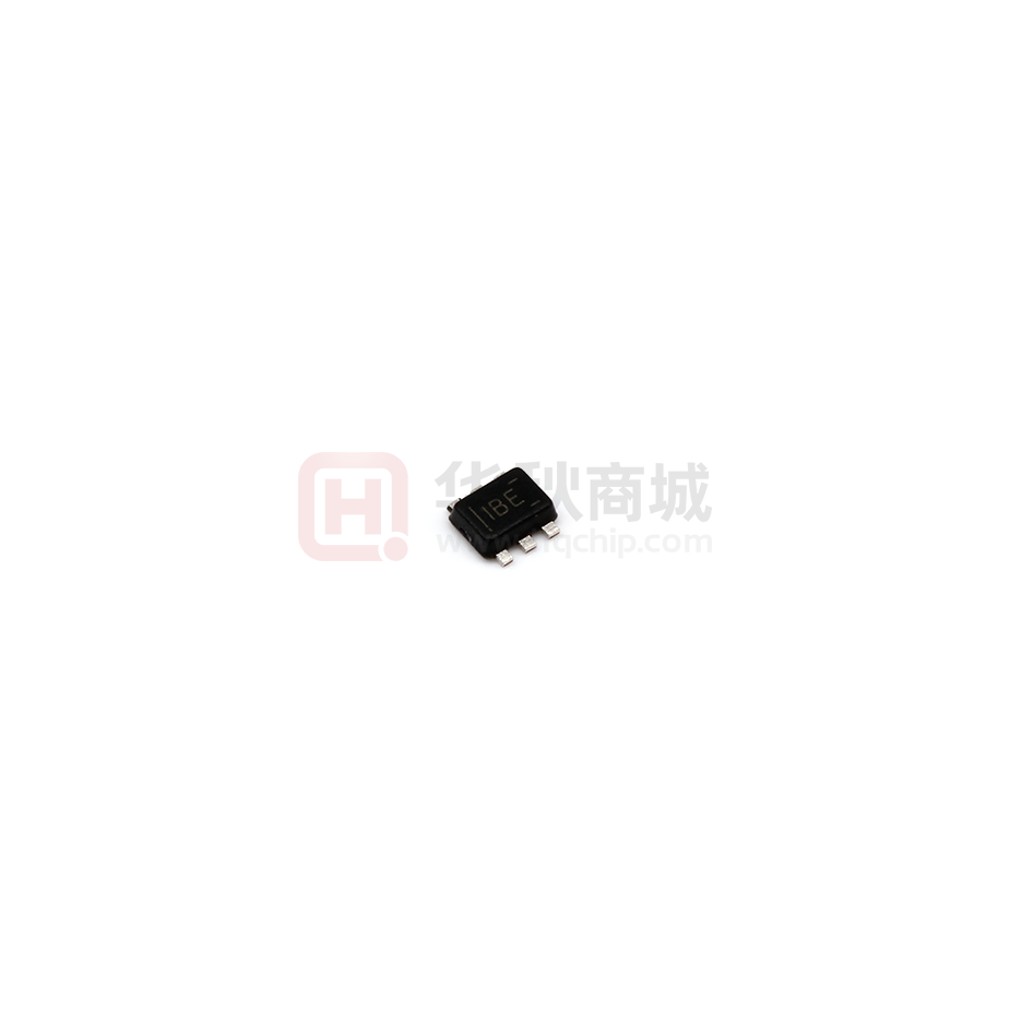
TLV62568ADRLR
ACTIVE
SOT-5X3
DRL
6
3000
RoHS & Green
Call TI | SN
Level-1-260C-UNLIM
-40 to 125
1BE
TLV62568ADRLT
ACTIVE
SOT-5X3
DRL
6
250
RoHS & Green
Call TI | SN
Level-1-260C-UNLIM
-40 to 125
1BE
TLV62568APDRLR
ACTIVE
SOT-5X3
DRL
6
3000
RoHS & Green
Call TI | SN
Level-1-260C-UNLIM
-40 to 125
1BF
TLV62568APDRLT
ACTIVE
SOT-5X3
DRL
6
250
RoHS & Green
Call TI | SN
Level-1-260C-UNLIM
-40 to 125
1BF
TLV62569ADRLR
ACTIVE
SOT-5X3
DRL
6
3000
RoHS & Green
Call TI | SN
Level-1-260C-UNLIM
-40 to 125
1BG
TLV62569ADRLT
ACTIVE
SOT-5X3
DRL
6
250
RoHS & Green
Call TI | SN
Level-1-260C-UNLIM
-40 to 125
1BG
TLV62569APDRLR
ACTIVE
SOT-5X3
DRL
6
3000
RoHS & Green
Call TI | SN
Level-1-260C-UNLIM
-40 to 125
1BH
TLV62569APDRLT
ACTIVE
SOT-5X3
DRL
6
250
RoHS & Green
Call TI | SN
Level-1-260C-UNLIM
-40 to 125
1BH
(1)
The marketing status values are defined as follows:
ACTIVE: Product device recommended for new designs.
LIFEBUY: TI has announced that the device will be discontinued, and a lifetime-buy period is in effect.
NRND: Not recommended for new designs. Device is in production to support existing customers, but TI does not recommend using this part in a new design.
PREVIEW: Device has been announced but is not in production. Samples may or may not be available.
OBSOLETE: TI has discontinued the production of the device.
(2)
RoHS: TI defines "RoHS" to mean semiconductor products that are compliant with the current EU RoHS requirements for all 10 RoHS substances, including the requirement that RoHS substance
do not exceed 0.1% by weight in homogeneous materials. Where designed to be soldered at high temperatures, "RoHS" products are suitable for use in specified lead-free processes. TI may
reference these types of products as "Pb-Free".
RoHS Exempt: TI defines "RoHS Exempt" to mean products that contain lead but are compliant with EU RoHS pursuant to a specific EU RoHS exemption.
Green: TI defines "Green" to mean the content of Chlorine (Cl) and Bromine (Br) based flame retardants meet JS709B low halogen requirements of


 工商网监
湘ICP备2023018690号
工商网监
湘ICP备2023018690号

