Order
Now
Product
Folder
Support &
Community
Tools &
Software
Technical
Documents
TLV707, TLV707P
SBVS153F – FEBRUARY 2011 – REVISED MAY 2018
TLV707, TLV707P
200-mA, Low-IQ, Low-Noise, Low-Dropout Regulator for Portable Devices
1 Features
3 Description
•
•
•
•
The TLV707 series (TLV707 and TLV707P) of lowdropout linear regulators (LDOs) are low quiescent
current devices with excellent line and load transient
performance for power-sensitive applications. These
devices provide a typical accuracy of 0.5%. All
versions have thermal shutdown and overcurrent
protection for safety.
1
•
•
•
•
0.5% Typical Accuracy
Supports 200-mA Output
Low IQ: 25 μA
Fixed-Output Voltage Combinations Possible from
0.85 V to 5.0 V(1)
High PSRR:
– 70 dB at 100 Hz
– 50 dB at 1 MHz
Stable With Effective Capacitance of 0.1 μF(2)
Thermal Shutdown and Overcurrent Protection
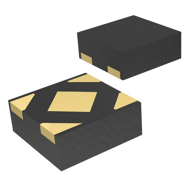
Package: 1-mm × 1-mm DQN (X2SON)
Furthermore, these devices are stable with an
effective output capacitance of only 0.1 µF. This
feature enables the use of cost-effective capacitors
that have higher bias voltages and temperature
derating. These devices also regulate to the specified
accuracy with no output load.
The TLV707P also provides an active pulldown circuit
to quickly discharge the outputs.
(1)
For all available voltage options, see the package option
addendum at the end of the data sheet.
(2)
See the Mechanical, Packaging, and Orderable Information
section for more details.
The TLV707 series of LDOs are available in a 1-mm
× 1-mm DQN (X2SON) package that makes them
desirable for handheld applications.
2 Applications
•
•
•
•
•
Device Information(1)
Smart Phones and Wireless Handsets
Gaming and Toys
WLAN and Other PC Add-On Cards
TVs and Set-Top Boxes
Wearable Electronics
PART NUMBER
TLV707
TLV707P
PACKAGE
X2SON (4)
BODY SIZE (NOM)
1.00 mm × 1.00 mm
(1) For all available packages, see the package option addendum
at the end of the datasheet.
Typical Application Circuit
VIN
IN
OUT
CIN
COUT
VOUT
1 mF
Ceramic
TLV707 Series
On
Off
EN
GND
1
An IMPORTANT NOTICE at the end of this data sheet addresses availability, warranty, changes, use in safety-critical applications,
intellectual property matters and other important disclaimers. PRODUCTION DATA.
�TLV707, TLV707P
SBVS153F – FEBRUARY 2011 – REVISED MAY 2018
www.ti.com
Table of Contents
1
2
3
4
5
6
7
Features ..................................................................
Applications ...........................................................
Description .............................................................
Revision History.....................................................
Pin Configuration and Functions .........................
Specifications.........................................................
1
1
1
2
4
5
6.1
6.2
6.3
6.4
6.5
6.6
5
5
5
5
6
7
Detailed Description ............................................ 17
7.1
7.2
7.3
7.4
8
Absolute Maximum Ratings ......................................
ESD Ratings..............................................................
Recommended Operating Conditions.......................
Thermal Information ..................................................
Electrical Characteristics...........................................
Typical Characteristics ..............................................
Overview .................................................................
Functional Block Diagrams .....................................
Feature Description.................................................
Device Functional Modes........................................
17
17
18
19
Application and Implementation ........................ 20
8.1 Application Information............................................ 20
8.2 Typical Application .................................................. 20
8.3 Do's and Don'ts ....................................................... 23
9 Power Supply Recommendations...................... 24
10 Layout................................................................... 24
10.1
10.2
10.3
10.4
Layout Guidelines .................................................
Layout Example ....................................................
Thermal Considerations ........................................
Power Dissipation .................................................
24
24
24
25
11 Device and Documentation Support ................. 26
11.1
11.2
11.3
11.4
11.5
11.6
11.7
11.8
Device Support......................................................
Documentation Support ........................................
Related Links ........................................................
Receiving Notification of Documentation Updates
Community Resources..........................................
Trademarks ...........................................................
Electrostatic Discharge Caution ............................
Glossary ................................................................
26
26
26
26
27
27
27
27
12 Mechanical, Packaging, and Orderable
Information ........................................................... 27
4 Revision History
NOTE: Page numbers for previous revisions may differ from page numbers in the current version.
Changes from Revision E (February 2016) to Revision F
•
Page
Changed V(ESD) HBM value from ±2000 V to ±4000 V in ESD Ratings table......................................................................... 5
Changes from Revision D (January 2015) to Revision E
Page
•
Changed device name to TLV707, TLV707P and changed VIN, VOUT(nom), IOUT symbols throughout document.................... 1
•
Changed DQN package designator name in Package Features bullet ................................................................................. 1
•
Changed Applications bullets ................................................................................................................................................ 1
•
Deleted first sentence from last paragraph of Description section ........................................................................................ 1
•
Changed caption of front-page figure .................................................................................................................................... 1
•
Changed Thermal Information table ....................................................................................................................................... 5
•
Changed TA to TJ in conditions of Electrical Characteristics table ........................................................................................ 6
•
Deleted temperature test conditions from VOUT parameter in Electrical Characteristics table .............................................. 6
•
Deleted UVLO parameter from Electrical Characteristics table ............................................................................................ 6
•
Deleted UVLO block from Figure 58 ................................................................................................................................... 18
•
Added cross-reference for Equation 1 ................................................................................................................................. 19
•
Changed Device Functional Modes section ........................................................................................................................ 19
•
Deleted Undervoltage Lockout (UVLO) section .................................................................................................................. 19
•
Changed title of Figure 59 ................................................................................................................................................... 20
•
Added cross-reference for Table 1 ...................................................................................................................................... 20
•
Added cross-reference for Figure 68 ................................................................................................................................... 24
2
Submit Documentation Feedback
Copyright © 2011–2018, Texas Instruments Incorporated
Product Folder Links: TLV707 TLV707P
�TLV707, TLV707P
www.ti.com
SBVS153F – FEBRUARY 2011 – REVISED MAY 2018
Changes from Revision C (November 2012) to Revision D
Page
•
Changed references to DFN (SON) package to DQN (X2SON) throughout document ........................................................ 1
•
Changed Features list bullets ................................................................................................................................................ 1
•
Changed fourth paragraph of Description section ................................................................................................................. 1
•
Added ESD Ratings table, Feature Description section, Device Functional Modes, Application and Implementation
section, Power Supply Recommendations section, Layout section, Device and Documentation Support section, and
Mechanical, Packaging, and Orderable Information section ................................................................................................. 1
•
Changed Pin Descriptions table contents ............................................................................................................................. 4
•
Changed Overview section .................................................................................................................................................. 17
•
Changed Internal Current Limit section ............................................................................................................................... 18
•
Changed Input and Output Capacitor Requirements section .............................................................................................. 20
Changes from Revision B (October 2011) to Revision C
Page
•
Changed voltage range in fourth Features bullet ................................................................................................................... 1
•
Changed front page pinout drawing ....................................................................................................................................... 1
•
Changed Output voltage range parameter minimum specification in Electrical Characteristics table ................................... 6
•
Changed DC output accuracy parameter test conditions in Electrical Characteristics table ................................................. 6
•
Changed voltage range in footnote 2 of Ordering Information table .................................................................................... 26
Changes from Revision A (August 2011) to Revision B
Page
•
Deleted reference to DCK package from Features ................................................................................................................ 1
•
Deleted DCK package pinout drawing.................................................................................................................................... 1
•
Deleted column for DCK package from Pin Descriptions table.............................................................................................. 4
•
Deleted DCK package from Thermal Information table.......................................................................................................... 5
Changes from Original (February 2011) to Revision A
Page
•
Added footnote to Features to show available voltage options.............................................................................................. 1
•
Added preview banner over DCK pinout drawing .................................................................................................................. 1
Submit Documentation Feedback
Copyright © 2011–2018, Texas Instruments Incorporated
Product Folder Links: TLV707 TLV707P
3
�TLV707, TLV707P
SBVS153F – FEBRUARY 2011 – REVISED MAY 2018
www.ti.com
5 Pin Configuration and Functions
DQN Package
4-Pin X2SON
Top View
IN
4
EN
3
Thermal
Pad
1
2
OUT
GND
Pin Functions
PIN
NAME
NO.
I/O
DESCRIPTION
Enable pin. Driving EN over 0.9 V turns on the regulator. Driving EN below 0.4 V puts the
regulator into shutdown mode.
For TLV707P, output voltage is discharged through an internal 120-Ω resistor when device is
shut down.
EN
3
I
GND
2
—
IN
4
I
Input pin. For good transient performance, place a small 1-µF ceramic capacitor from this pin to
ground. See Input and Output Capacitor Requirements for more details.
OUT
1
O
Regulated output voltage pin. A small 1-μF ceramic capacitor is required from this pin to ground
to assure stability. See Input and Output Capacitor Requirements for more details.
4
Ground pin
Submit Documentation Feedback
Copyright © 2011–2018, Texas Instruments Incorporated
Product Folder Links: TLV707 TLV707P
�TLV707, TLV707P
www.ti.com
SBVS153F – FEBRUARY 2011 – REVISED MAY 2018
6 Specifications
6.1 Absolute Maximum Ratings
over operating junction temperature range (unless otherwise noted) (1)
Voltage
(2)
Current (source)
MIN
MAX
UNIT
IN
–0.3
6.0
V
EN
–0.3
6.0
V
OUT
–0.3
6.0
V
OUT
Internally limited
Output short-circuit duration
Temperature
(1)
(2)
Indefinite
Operating junction, TJ
–55
150
°C
Storage, Tstg
–55
150
°C
Stresses beyond those listed under Absolute Maximum Ratings may cause permanent damage to the device. These are stress ratings
only, and functional operation of the device at these or any other conditions beyond those indicated under Recommended Operating
Conditions is not implied. Exposure to absolute-maximum-rated conditions for extended periods my affect device reliability.
All voltages are with respect to network ground pin.
6.2 ESD Ratings
VALUE
V(ESD)
(1)
(2)
Electrostatic discharge
Human body model (HBM) QSS 009-105 (JESD22-A114A)
(1)
UNIT
±4000
Charged device model (CDM) QSS 009-147 (JESD22-C101B.01) (2)
V
±500
JEDEC document JEP155 states that 500-V HBM allows safe manufacturing with a standard ESD control process.
JEDEC document JEP157 states that 250-V CDM allows safe manufacturing with a standard ESD control process.
6.3 Recommended Operating Conditions
over operating junction temperature range (unless otherwise noted)
MIN
VIN
Input voltage
IOUT
Output current
TJ
Operating junction temperature
NOM
MAX
UNIT
2.0
5.5
V
0
200
mA
–40
125
°C
6.4 Thermal Information
TLV707, TLV707P
THERMAL METRIC (1)
DQN (X2SON)
UNIT
4 PINS
RθJA
Junction-to-ambient thermal resistance
208.1
°C/W
RθJC(top)
Junction-to-case (top) thermal resistance
108.8
°C/W
RθJB
Junction-to-board thermal resistance
159.4
°C/W
ψJT
Junction-to-top characterization parameter
3.8
°C/W
ψJB
Junction-to-board characterization parameter
159.4
°C/W
RθJC(bot)
Junction-to-case (bottom) thermal resistance
110.2
°C/W
(1)
For more information about traditional and new thermal metrics, see the Semiconductor and IC Package Thermal Metrics application
report.
Submit Documentation Feedback
Copyright © 2011–2018, Texas Instruments Incorporated
Product Folder Links: TLV707 TLV707P
5
�TLV707, TLV707P
SBVS153F – FEBRUARY 2011 – REVISED MAY 2018
www.ti.com
6.5 Electrical Characteristics
At VIN = VOUT(nom) + 0.5 V or 2.0 V (whichever is greater); IOUT = 1 mA, VEN = VIN, COUT = 0.47 μF, and TJ = –40°C to +85°C
(unless otherwise noted). Typical values are at TJ = 25°C.
PARAMETER
TEST CONDITIONS
MIN
Output voltage range
VOUT
DC output accuracy
ΔVO(ΔVI)
Line regulation
ΔVO(ΔIO)
Load regulation
5
–1.5%
0 mA ≤ IOUT ≤ 150 mA
2.4 V < VOUT ≤ 2.8 V
Dropout voltage
MAX
UNIT
V
0.5%
VOUT ≥ 0.85 V
2.0 V < VOUT ≤ 2.4 V
V(DO)
TYP
0.85
VIN = 0.98 x
VOUT(nom)
2.8 V < VOUT ≤ 3.3 V
3.3 V < VOUT ≤ 5.0 V
1.5%
1
5
mV
10
20
mV
IOUT = 30 mA
65
IOUT = 150 mA
325
IOUT = 30 mA
50
IOUT = 150 mA
250
IOUT = 30 mA
45
IOUT = 150 mA
220
360
300
mV
270
IOUT = 30 mA
40
IOUT = 150 mA
200
250
300
450
mA
50
µA
ICL
Output current limit
VOUT = 0.9 × VOUT(nom)
I(GND)
Ground pin current
IOUT = 0 mA
25
I(EN)
EN pin current
VEN = 5.5 V
0.01
µA
ISHUTDOWN
Shutdown current
VEN ≤ 0.4 V, 2.0 V ≤ VIN ≤ 4.5 V
1
µA
VIL(EN)
EN pin low-level input
voltage (disable device)
0
0.4
V
VIH(EN)
EN pin high-level input
voltage (enable device)
0.9
VIN
V
PSRR
Power-supply rejection
ratio
VIN = 3.3 V, VOUT = 2.8 V,
IOUT = 30 mA
240
f = 100 Hz
70
f = 10 kHz
55
f = 1 MHz
50
Vn
Output noise voltage
BW = 100 Hz to 100 kHz, VIN = 2.3 V, VOUT = 1.8 V,
IOUT = 10 mA
tSTR
Startup time (1)
COUT = 1.0 µF, IOUT = 150 mA
RPULLDOWN
Pulldown resistance
(TLV707P only)
(1)
6
dB
45
µVRMS
100
µs
120
Ω
Startup time = time from EN assertion to 0.98 × Vout.
Submit Documentation Feedback
Copyright © 2011–2018, Texas Instruments Incorporated
Product Folder Links: TLV707 TLV707P
�TLV707, TLV707P
www.ti.com
SBVS153F – FEBRUARY 2011 – REVISED MAY 2018
6.6 Typical Characteristics
1.3
2.9
1.28
2.88
1.26
2.86
Output Voltage (V)
Output Voltage (V)
At TJ = –40°C to +85°C, VIN = VOUT(nom) + 0.5 V or 2.0 V (whichever is greater), IOUT = 10 mA, VEN = VIN, and COUT = 1 μF,
unless otherwise noted. Typical values are at TJ = 25°C.
1.24
1.22
1.2
1.18
1.16
85°C
25°C
-40°C
1.14
1.12
2.84
2.82
2.8
2.78
2.76
85°C
25°C
-40°C
2.74
2.72
1.1
2.7
0
20
40
60
80 100 120 140 160 180
Output Current (mA)
200
0
20
40
60
VOUT = 1.2 V
Figure 2. Load Regulation
5.1
1.3
5.08
1.28
5.06
1.26
Output Voltage (V)
Output Voltage (V)
200
VOUT = 2.8 V
Figure 1. Load Regulation
5.04
5.02
5
4.98
4.96
85°C
25°C
-40°C
4.94
4.92
1.24
1.22
1.2
1.18
1.16
85°C
25°C
-40°C
1.14
1.12
4.9
1.1
0
20
40
60
80 100 120 140 160 180
Output Current (mA)
200
2
2.5
VOUT = 5.0 V
3
3.5
4
Input Voltage (V)
4.5
5
5.5
VOUT = 1.2 V, IOUT = 10 mA
Figure 3. Load Regulation
Figure 4. Line Regulation
2.9
5.1
2.88
5.08
2.86
5.06
Output Voltage (V)
Output Voltage (V)
80 100 120 140 160 180
Output Current (mA)
2.84
2.82
2.8
2.78
2.76
85°C
25°C
-40°C
2.74
2.72
5.04
5.02
5
4.98
4.96
85°C
25°C
-40°C
4.94
4.92
4.9
2.7
3.1
3.7
4.3
Input Voltage (V)
4.9
5.5
5.3
VOUT = 2.8 V, IOUT = 10 mA
5.35
5.4
Input Voltage (V)
5.45
5.5
VOUT = 5.0 V, IOUT = 10 mA
Figure 5. Line Regulation
Figure 6. Line Regulation
Submit Documentation Feedback
Copyright © 2011–2018, Texas Instruments Incorporated
Product Folder Links: TLV707 TLV707P
7
�TLV707, TLV707P
SBVS153F – FEBRUARY 2011 – REVISED MAY 2018
www.ti.com
Typical Characteristics (continued)
1.3
2.9
1.28
2.88
1.26
2.86
Output Voltage (V)
Output Voltage (V)
At TJ = –40°C to +85°C, VIN = VOUT(nom) + 0.5 V or 2.0 V (whichever is greater), IOUT = 10 mA, VEN = VIN, and COUT = 1 μF,
unless otherwise noted. Typical values are at TJ = 25°C.
1.24
1.22
1.2
1.18
1.16
85°C
25°C
-40°C
1.14
1.12
2.84
2.82
2.8
2.78
2.76
85°C
25°C
-40°C
2.74
2.72
1.1
2.7
2
2.5
3
3.5
4
Input Voltage (V)
4.5
5
5.5
3.1
3.7
VOUT = 1.2 V, IOUT = 150 mA
5.1
1.3
5.08
1.28
5.06
1.26
Output Voltage (V)
Output Voltage (V)
5.5
Figure 8. Line Regulation
5.04
5.02
5
4.98
4.96
85°C
25°C
-40°C
4.94
4.92
1.24
1.22
1.2
1.18
1.16
1.14
IOUT = 10 mA
IOUT = 150 mA
1.12
4.9
1.1
5.3
5.35
5.4
Input Voltage (V)
5.45
5.5
-40
-15
VOUT = 5.0 V, IOUT = 150 mA
10
35
Temperature (°C)
60
85
VOUT = 1.2 V
Figure 9. Line Regulation
Figure 10. Output Voltage vs Temperature
2.9
5.1
2.88
5.08
2.86
5.06
Output Voltage (V)
Output Voltage (V)
4.9
VOUT = 2.8 V, IOUT = 150 mA
Figure 7. Line Regulation
2.84
2.82
2.8
2.78
2.76
2.74
5.04
5.02
5
4.98
4.96
4.94
IOUT = 10 mA
IOUT = 150 mA
2.72
IOUT = 10 mA
IOUT = 150 mA
4.92
2.7
4.9
-40
-15
10
35
Temperature (°C)
60
85
-40
-15
VOUT = 2.8 V
10
35
Temperature (°C)
60
85
VOUT = 5.0 V
Figure 11. Output Voltage vs Temperature
8
4.3
Input Voltage (V)
Figure 12. Output Voltage vs Temperature
Submit Documentation Feedback
Copyright © 2011–2018, Texas Instruments Incorporated
Product Folder Links: TLV707 TLV707P
�TLV707, TLV707P
www.ti.com
SBVS153F – FEBRUARY 2011 – REVISED MAY 2018
Typical Characteristics (continued)
At TJ = –40°C to +85°C, VIN = VOUT(nom) + 0.5 V or 2.0 V (whichever is greater), IOUT = 10 mA, VEN = VIN, and COUT = 1 μF,
unless otherwise noted. Typical values are at TJ = 25°C.
600
400
500
300
Dropout Voltage (mV)
Dropout Voltage (mV)
350
250
200
150
100
85°C
25°C
-40°C
50
400
300
200
85°C
25°C
-40°C
100
0
0
2
2.5
3
3.5
4
Input Voltage (V)
4.5
2
5
2.5
3
IOUT = 150 mA
5
Figure 14. Dropout Voltage vs Input Voltage
350
350
300
300
Dropout Voltage (mV)
Dropout Voltage (mV)
4.5
IOUT = 200 mA
Figure 13. Dropout Voltage vs Input Voltage
250
200
150
100
85°C
25°C
-40°C
50
250
200
150
100
85°C
25°C
-40°C
50
0
0
0
20
40
60
80 100 120 140 160 180
Output Current (mA)
200
0
20
40
60
VOUT = 2.8 V
80 100 120 140 160 180
Output Current (mA)
200
VOUT = 5.0 V
Figure 15. Dropout Voltage vs Output Current
Figure 16. Dropout Voltage vs Output Current
35
35
30
30
25
20
15
10
85°C
25°C
-40°C
5
0
Ground Pin Current (mA)
Ground Pin Current (mA)
3.5
4
Input Voltage (V)
25
20
15
10
85°C
25°C
-40°C
5
0
2
2.5
3
3.5
4
Input Voltage (V)
4.5
5
5.5
3.1
VOUT = 1.2 V, IOUT = 0 mA
3.7
4.3
Input Voltage (V)
4.9
5.5
VOUT = 2.8 V, IOUT = 0 mA
Figure 17. Ground Pin Current vs Input Voltage
Figure 18. Ground Pin Current vs Input Voltage
Submit Documentation Feedback
Copyright © 2011–2018, Texas Instruments Incorporated
Product Folder Links: TLV707 TLV707P
9
�TLV707, TLV707P
SBVS153F – FEBRUARY 2011 – REVISED MAY 2018
www.ti.com
Typical Characteristics (continued)
35
40
30
35
Ground Pin Current (mA)
Ground Pin Current (mA)
At TJ = –40°C to +85°C, VIN = VOUT(nom) + 0.5 V or 2.0 V (whichever is greater), IOUT = 10 mA, VEN = VIN, and COUT = 1 μF,
unless otherwise noted. Typical values are at TJ = 25°C.
25
20
15
10
85°C
25°C
-40°C
5
30
25
20
15
10
5
0
0
5.3
5.35
5.4
Input Voltage (V)
5.45
5.5
-40
VOUT = 5.0 V, IOUT = 0 mA
40
40
35
35
Ground Pin Current (mA)
Ground Pin Current (mA)
85
Figure 20. Ground Pin Current vs Temperature
30
25
20
15
10
5
30
25
20
15
10
5
0
0
-40
10
35
Temperature (°C)
-15
60
85
-40
60
85
VOUT = 5.0 V, IOUT = 0 mA
Figure 21. Ground Pin Current vs Temperature
Figure 22. Ground Pin Current vs Temperature
1200
1000
1000
800
600
400
85°C
25°C
-40°C
0
Ground Pin Current (mA)
1200
200
10
35
Temperature (°C)
-15
VOUT = 2.8 V, IOUT = 0 mA
Ground Pin Current (mA)
60
VOUT = 1.2 V, IOUT = 0 mA
Figure 19. Ground Pin Current vs Input Voltage
800
600
400
85°C
25°C
-40°C
200
0
0
20
40
60
80 100 120 140 160 180
Output Current (mA)
200
0
20
VOUT = 1.2 V
40
60
80 100 120 140 160 180
Output Current (mA)
200
VOUT = 2.8 V
Figure 23. Ground Pin Current vs Output Current
10
10
35
Temperature (°C)
-15
Figure 24. Ground Pin Current vs Output Current
Submit Documentation Feedback
Copyright © 2011–2018, Texas Instruments Incorporated
Product Folder Links: TLV707 TLV707P
�TLV707, TLV707P
www.ti.com
SBVS153F – FEBRUARY 2011 – REVISED MAY 2018
Typical Characteristics (continued)
At TJ = –40°C to +85°C, VIN = VOUT(nom) + 0.5 V or 2.0 V (whichever is greater), IOUT = 10 mA, VEN = VIN, and COUT = 1 μF,
unless otherwise noted. Typical values are at TJ = 25°C.
1200
2
1000
Shutdown Current (mA)
Ground Pin Current (mA)
1.8
800
600
400
85°C
25°C
-40°C
200
1.6
1.4
1.2
1
0.8
0.6
85°C
25°C
-40°C
0.4
0.2
0
0
0
20
40
60
80 100 120 140 160 180
Output Current (mA)
200
2
2.5
3
VOUT = 5.0 V
5
5.5
Figure 26. Shutdown Current vs Input Voltage
2
2
1.8
1.8
1.6
1.6
1.4
1.2
1
0.8
0.6
85°C
25°C
-40°C
0.4
0.2
Shutdown Current (mA)
Shutdown Current (mA)
4.5
VOUT = 1.2 V
Figure 25. Ground Pin Current vs Output Current
1.4
1.2
1
0.8
0.6
85°C
25°C
-40°C
0.4
0.2
0
0
2
2.5
3
3.5
4
Input Voltage (V)
4.5
5
5.5
2
2.5
3
VOUT = 2.8 V
3.5
4
Input Voltage (V)
4.5
5
5.5
VOUT = 5.0 V
Figure 27. Shutdown Current vs Input Voltage
Figure 28. Shutdown Current vs Input Voltage
450
450
425
425
400
400
Current Limit (mA)
Current Limit (mA)
3.5
4
Input Voltage (V)
375
350
325
375
350
325
300
300
25°C
-40°C
275
25°C
-40°C
275
250
250
2
2.5
3
3.5
4
Input Voltage (V)
4.5
5
5.5
3.1
3.7
VOUT = 1.2 V
4.3
Input Voltage (V)
4.9
5.5
VOUT = 2.8 V
Figure 29. Current Limit vs Input Voltage
Figure 30. Current Limit vs Input Voltage
Submit Documentation Feedback
Copyright © 2011–2018, Texas Instruments Incorporated
Product Folder Links: TLV707 TLV707P
11
�TLV707, TLV707P
SBVS153F – FEBRUARY 2011 – REVISED MAY 2018
www.ti.com
Typical Characteristics (continued)
At TJ = –40°C to +85°C, VIN = VOUT(nom) + 0.5 V or 2.0 V (whichever is greater), IOUT = 10 mA, VEN = VIN, and COUT = 1 μF,
unless otherwise noted. Typical values are at TJ = 25°C.
450
Power-Supply Ripple Rejection (dB)
90
Current Limit (mA)
425
400
375
350
325
300
25°C
-40°C
275
250
80
70
60
50
40
30
20
IOUT = 30 mA
IOUT = 150 mA
10
0
3.1
3.7
4.3
Input Voltage (V)
4.9
5.5
10
100
VOUT = 5.0 V
10M
90
Power-Supply Ripple Rejection (dB)
Power-Supply Ripple Rejection (dB)
1M
Figure 32. Power-Supply Ripple Rejection vs Frequency
90
80
70
60
50
40
30
20
IOUT = 30 mA
IOUT = 150 mA
10
0
80
70
60
50
40
30
20
IOUT = 30 mA
IOUT = 150 mA
10
0
10
100
1k
10k
100k
Frequency (Hz)
1M
10M
10
100
VOUT = 2.8 V
1k
10k
100k
Frequency (Hz)
1M
10M
VOUT = 5.0 V
Figure 33. Power-Supply Ripple Rejection vs Frequency
Figure 34. Power-Supply Ripple Rejection vs Frequency
70
60
50
40
30
20
10
1 kHz
1 MHz
0
Power-Supply Ripple Rejection (dB)
70
Power-Supply Ripple Rejection (dB)
10k
100k
Frequency (Hz)
VOUT = 1.2 V
Figure 31. Current Limit vs Input Voltage
60
50
40
30
20
10
1 kHz
1 MHz
0
3.1
3.2
3.3
3.4
3.5
Input Voltage (V)
3.6
3.7
3.8
3.1
3.2
VOUT = 2.8 V, IOUT = 30 mA
3.3
3.4
3.5
Input Voltage (V)
3.6
3.7
3.8
VOUT = 2.8 V, IOUT = 150 mA
Figure 35. Power-Supply Ripple Rejection vs Input Voltage
12
1k
Figure 36. Power-Supply Ripple Rejection vs Input Voltage
Submit Documentation Feedback
Copyright © 2011–2018, Texas Instruments Incorporated
Product Folder Links: TLV707 TLV707P
�TLV707, TLV707P
www.ti.com
SBVS153F – FEBRUARY 2011 – REVISED MAY 2018
Typical Characteristics (continued)
At TJ = –40°C to +85°C, VIN = VOUT(nom) + 0.5 V or 2.0 V (whichever is greater), IOUT = 10 mA, VEN = VIN, and COUT = 1 μF,
unless otherwise noted. Typical values are at TJ = 25°C.
70
60
50
40
30
20
10
1 kHz
1 MHz
Power-Supply Ripple Rejection (dB)
Power-Supply Ripple Rejection (dB)
70
60
50
40
30
20
10
0
1 kHz
1 MHz
0
3.6
3.7
3.8
3.9
4
Input Voltage (V)
4.1
4.2
4.3
3.6
3.7
VOUT = 3.3 V, IOUT = 30 mA
3.9
4
Input Voltage (V)
4.1
4.2
4.3
VOUT = 3.3 V, IOUT = 150 mA
100
5V
2.8 V
1.2 V
10
Figure 38. Power-Supply Ripple Rejection vs Input Voltage
150 mA
100 mA/div
Figure 37. Power-Supply Ripple Rejection vs Input Voltage
50 mA
IOUT
1
50 mV/div
Output Spectral Noise Density (mV/ÖHz)
3.8
0.1
VOUT
0.01
0.001
10
100
1k
10k
100k
Frequency (Hz)
1M
Time (100 ms/div)
10M
VOUT = 1.2 V
50 mV/div
1 mA
IOUT
VOUT
100 mA
50 mA/div
150 mA
Figure 40. Load Transient Response
50 mA
50 mV/div
200 mA/div
Figure 39. Output Spectral Noise Density vs Frequency
VOUT
Time (100 ms/div)
Time (100 ms/div)
VOUT = 1.2 V
VOUT = 2.8 V
Figure 41. Load Transient Response
IOUT
Figure 42. Load Transient Response
Submit Documentation Feedback
Copyright © 2011–2018, Texas Instruments Incorporated
Product Folder Links: TLV707 TLV707P
13
�TLV707, TLV707P
SBVS153F – FEBRUARY 2011 – REVISED MAY 2018
www.ti.com
Typical Characteristics (continued)
At TJ = –40°C to +85°C, VIN = VOUT(nom) + 0.5 V or 2.0 V (whichever is greater), IOUT = 10 mA, VEN = VIN, and COUT = 1 μF,
unless otherwise noted. Typical values are at TJ = 25°C.
50 mV/div
IOUT
VOUT
50 mA/div
1 mA
100 mA
VOUT
Time (100 ms/div)
Time (100 ms/div)
VOUT = 2.8 V
VOUT = 5.0 V
Figure 43. Load Transient Response
Figure 44. Load Transient Response
100 mV/div
1 mA
IOUT
1 V/div
100 mA/div
150 mA
VIN
10 mV/div
VOUT
VOUT
Time (100 ms/div)
Time (100 ms/div)
VOUT = 5.0 V
VOUT = 1.2 V, IOUT = 150 mA
20 mV/div
VIN
VOUT
2 V/div
Figure 46. Line Transient Response
VIN
VOUT
20 mV/div
1 V/div
Figure 45. Load Transient Response
Time (100 ms/div)
Time (100 ms/div)
VOUT = 1.2 V, IOUT = 200 mA
VOUT = 1.2 V, IOUT = 150 mA
Figure 47. Line Transient Response
14
IOUT
50 mA
50 mV/div
100 mA/div
150 mA
Figure 48. Line Transient Response
Submit Documentation Feedback
Copyright © 2011–2018, Texas Instruments Incorporated
Product Folder Links: TLV707 TLV707P
�TLV707, TLV707P
www.ti.com
SBVS153F – FEBRUARY 2011 – REVISED MAY 2018
Typical Characteristics (continued)
20 mV/div
VOUT
VIN
10 mV/div
2 V/div
VIN
1 V/div
At TJ = –40°C to +85°C, VIN = VOUT(nom) + 0.5 V or 2.0 V (whichever is greater), IOUT = 10 mA, VEN = VIN, and COUT = 1 μF,
unless otherwise noted. Typical values are at TJ = 25°C.
VOUT
Time (100 ms/div)
Time (100 ms/div)
VOUT = 1.2 V, IOUT = 200 mA
VOUT = 2.8 V, IOUT = 150 mA
10 mV/div
VIN
VOUT
1 V/div
Figure 50. Line Transient Response
VIN
VOUT
20 mV/div
1 V/div
Figure 49. Line Transient Response
Time (100 ms/div)
Time (100 ms/div)
VOUT = 2.8 V, IOUT = 200 mA
VOUT = 2.8 V, IOUT = 200 mA
1 V/div
Figure 51. Line Transient Response
Figure 52. Line Transient Response
VIN
2 V/div
VI
VOUT
20 mV/div
VO
Time (100 ms/div)
Time (100 ms/div)
VOUT = 2.8 V, IOUT = 200 mA
VOUT = 1.2 V, IOUT = 30 mA
Figure 53. Line Transient Response
Figure 54. VIN Ramp Up, Ramp Down Response
Submit Documentation Feedback
Copyright © 2011–2018, Texas Instruments Incorporated
Product Folder Links: TLV707 TLV707P
15
�TLV707, TLV707P
SBVS153F – FEBRUARY 2011 – REVISED MAY 2018
www.ti.com
Typical Characteristics (continued)
At TJ = –40°C to +85°C, VIN = VOUT(nom) + 0.5 V or 2.0 V (whichever is greater), IOUT = 10 mA, VEN = VIN, and COUT = 1 μF,
unless otherwise noted. Typical values are at TJ = 25°C.
VIN
1 V/div
1 V/div
VIN
VOUT
VOUT
Time (100 ms/div)
Time (100 ms/div)
VOUT = 2.8 V, IOUT = 30 mA
VOUT = 5 V, IOUT = 30 mA
Figure 55. VIN Ramp Up, Ramp Down Response
16
Figure 56. VIN Ramp Up, Ramp Down Response
Submit Documentation Feedback
Copyright © 2011–2018, Texas Instruments Incorporated
Product Folder Links: TLV707 TLV707P
�TLV707, TLV707P
www.ti.com
SBVS153F – FEBRUARY 2011 – REVISED MAY 2018
7 Detailed Description
7.1 Overview
The TLV707 series (TLV707 and TLV707P) belongs to a family of low-dropout regulators (LDOs). This device
consumes low quiescent current and delivers excellent line and load transient performance. These
characteristics, combined with low noise and very good PSRR with little (VIN – VOUT) headroom, make this device
ideal for portable RF applications.
7.2 Functional Block Diagrams
IN
OUT
Current
Limit
Thermal
Shutdown
EN
Bandgap
LOGIC
TLV707
GND
Figure 57. TLV707 Block Diagram
Submit Documentation Feedback
Copyright © 2011–2018, Texas Instruments Incorporated
Product Folder Links: TLV707 TLV707P
17
�TLV707, TLV707P
SBVS153F – FEBRUARY 2011 – REVISED MAY 2018
www.ti.com
Functional Block Diagrams (continued)
IN
OUT
Current
Limit
Thermal
Shutdown
120 W
EN
Bandgap
LOGIC
TLV707P
GND
Figure 58. TLV707P Block Diagram
7.3 Feature Description
This LDO regulator offers current limit and thermal protection. The operating junction temperature of this device
is –40°C to 125°C.
7.3.1 Internal Current Limit
The internal current limit helps to protect the regulator during fault conditions. During current limit, the output
sources a fixed amount of current that is largely independent of the output voltage. In such a case, the output
voltage is not regulated, and is VOUT = ILIMIT × RLOAD. The PMOS pass transistor dissipates (VIN – VOUT) × ILIMIT
until thermal shutdown is triggered and the device turns off. When the device cools, the internal thermal
shutdown circuit turns the device back on. If the fault condition continues, the device cycles between current limit
and thermal shutdown; see the Thermal Information table for more details.
The PMOS pass element has a built-in body diode that conducts current when the voltage at OUT exceeds the
voltage at IN. This current is not limited, so if extended reverse voltage operation is anticipated, external limiting
to 5% of the rated output current is recommended.
18
Submit Documentation Feedback
Copyright © 2011–2018, Texas Instruments Incorporated
Product Folder Links: TLV707 TLV707P
�TLV707, TLV707P
www.ti.com
SBVS153F – FEBRUARY 2011 – REVISED MAY 2018
Feature Description (continued)
7.3.2 Shutdown
The enable pin (EN) is active high. The device is enabled when voltage at the EN pin goes above 0.9 V. This
relatively lower voltage value required to turn on the LDO can also be used to power the device when it is
connected to a GPIO of a newer processor, where the GPIO Logic 1 voltage level is lower than that of traditional
microcontrollers. The device is turned off when the EN pin is held at less than 0.4 V. When shutdown capability
is not required, EN can be connected to the IN pin.
The TLV707P version has internal active pulldown circuitry that discharges the output with a time constant as
given by Equation 1:
(120 · RL)
t=
· COUT
(120 + RL)
where:
•
•
RL = Load resistance
COUT = Output capacitor
(1)
7.4 Device Functional Modes
The TLV707 series is specified over the recommended operating conditions (see the Recommended Operating
Conditions table). The specifications may not be met when exposed to conditions outside of the recommended
operating range.
In order to turn on the regulator, the EN pin must be driven over 0.9 V. Driving the EN pin below 0.4 V causes
the regulator to enter shutdown mode.
In shutdown, the current consumption of the device is reduced to 1 µA, typically.
Submit Documentation Feedback
Copyright © 2011–2018, Texas Instruments Incorporated
Product Folder Links: TLV707 TLV707P
19
�TLV707, TLV707P
SBVS153F – FEBRUARY 2011 – REVISED MAY 2018
www.ti.com
8 Application and Implementation
NOTE
Information in the following applications sections is not part of the TI component
specification, and TI does not warrant its accuracy or completeness. TI’s customers are
responsible for determining suitability of components for their purposes. Customers should
validate and test their design implementation to confirm system functionality.
8.1 Application Information
The TLV707 series is a low-dropout regulator (LDO) with low quiescent current that delivers excellent line and
load transient performance. This LDO regulator offers current limit and thermal protection. The operating junction
temperature of this device series is –40°C to 125°C.
8.2 Typical Application
VIN
IN
VOUT
1 mF
Ceramic
OUT
CIN
COUT
TLV707 Series
On
Off
EN
GND
Figure 59. Typical Application Circuit
8.2.1 Design Requirements
Provide an input supply with adequate headroom to meet minimum VIN requirements (as shown in Table 1),
compensate for the GND pin current, and to power the load.
Table 1. Design Parameters
PARAMETER
DESIGN REQUIREMENT
Input voltage
1.8 V - 3.6 V
Output voltage
1.2 V
Output current
100-mA
8.2.2 Detailed Design Procedure
8.2.2.1 Input and Output Capacitor Requirements
Generally, 1.0-µF X5R- and X7R-type ceramic capacitors are recommended because these capacitors have
minimal variation in value and equivalent series resistance (ESR) over temperature.
However, the TLV707 is designed to be stable with an effective capacitance of 0.1 µF or larger at the output.
Thus, the device is stable with capacitors of other dielectric types as well, as long as the effective capacitance
under operating bias voltage and temperature is greater than 0.1 µF. This effective capacitance refers to the
capacitance that the LDO detects under operating bias voltage and temperature conditions; that is, the
capacitance after taking both bias voltage and temperature derating into consideration. In addition to allowing the
use of less expensive dielectrics, this capability of being stable with 0.1-µF effective capacitance also enables the
use of smaller footprint capacitors that have higher derating in size- and space-constrained applications.
Using a 0.1-µF rated capacitor at the output of the LDO does not ensure stability because the effective
capacitance under the specified operating conditions is less than 0.1 µF. Maximum ESR must be less than
200 mΩ.
20
Submit Documentation Feedback
Copyright © 2011–2018, Texas Instruments Incorporated
Product Folder Links: TLV707 TLV707P
�TLV707, TLV707P
www.ti.com
SBVS153F – FEBRUARY 2011 – REVISED MAY 2018
Although an input capacitor is not required for stability, good analog design practice is to connect a 0.1-μF to
1.0-μF, low ESR capacitor across the IN pin and GND pin of the regulator. This capacitor counteracts reactive
input sources and improves transient response, noise rejection, and ripple rejection. A higher-value capacitor
may be necessary if large, fast rise-time load transients are anticipated, or if the device is not located close to the
power source. If source impedance is more than 2-Ω, a 0.1-μF input capacitor may be necessary to ensure
stability.
8.2.2.2 Dropout Voltage
The TLV707 series of LDOs use a PMOS pass transistor to achieve low dropout. When (VIN – VOUT) is less than
the dropout voltage (VDO), the PMOS pass device is in the linear region of operation and the input-to-output
resistance is the RDS(ON) of the PMOS pass element. VDO scales approximately with output current because the
PMOS device functions similar to a resistor in dropout.
As with any linear regulator, PSRR and transient response are degraded when (VIN – VOUT) approaches dropout.
8.2.2.3 Transient Response
As with any regulator, increasing the size of the output capacitor reduces over- and undershoot magnitude but
increases the duration of the transient response.
Submit Documentation Feedback
Copyright © 2011–2018, Texas Instruments Incorporated
Product Folder Links: TLV707 TLV707P
21
�TLV707, TLV707P
SBVS153F – FEBRUARY 2011 – REVISED MAY 2018
www.ti.com
Power-Supply Ripple Rejection (dB)
90
80
70
60
50
40
30
20
IOUT = 30 mA
IOUT = 150 mA
10
0
10
100
1k
10k
100k
Frequency (Hz)
1M
Output Spectral Noise Density (mV/ÖHz)
8.2.3 Application Curves
100
5V
2.8 V
1.2 V
10
1
0.1
0.01
0.001
10M
10
100
1k
10k
100k
Frequency (Hz)
1M
10M
VOUT = 1.2 V
200 mA/div
Figure 60. Power-Supply Ripple Rejection vs Frequency
Figure 61. Output Spectral Noise Density vs Frequency
150 mA
IOUT
50 mV/div
1 V/div
1 mA
VIN
10 mV/div
VOUT
VOUT
Time (100 ms/div)
Time (100 ms/div)
VOUT = 1.2 V
VOUT = 1.2 V, IOUT = 150 mA
20 mV/div
VIN
VOUT
2 V/div
Figure 63. Line Transient Response
VIN
VOUT
20 mV/div
1 V/div
Figure 62. Load Transient Response
Time (100 ms/div)
Time (100 ms/div)
VOUT = 1.2 V, IOUT = 200 mA
VOUT = 1.2 V, IOUT = 150 mA
Figure 64. Line Transient Response
22
Figure 65. Line Transient Response
Submit Documentation Feedback
Copyright © 2011–2018, Texas Instruments Incorporated
Product Folder Links: TLV707 TLV707P
�TLV707, TLV707P
www.ti.com
SBVS153F – FEBRUARY 2011 – REVISED MAY 2018
VIN
2 V/div
2 V/div
VIN
VOUT
20 mV/div
VOUT
Time (100 ms/div)
Time (100 ms/div)
VOUT = 1.2 V, IOUT = 200 mA
VOUT = 1.2 V, IOUT = 30 mA
Figure 66. Line Transient Response
Figure 67. VIN Ramp Up, Ramp Down Response
8.3 Do's and Don'ts
Place at least one 1.0-µF ceramic capacitor as close as possible to the OUT pin of the regulator.
Do not place the output capacitor more than 10 mm away from the regulator.
Connect a 1.0-μF low equivalent series resistance (ESR) capacitor across the IN pin and GND input of the
regulator for improved transient performance.
Do not exceed the absolute maximum ratings.
Submit Documentation Feedback
Copyright © 2011–2018, Texas Instruments Incorporated
Product Folder Links: TLV707 TLV707P
23
�TLV707, TLV707P
SBVS153F – FEBRUARY 2011 – REVISED MAY 2018
www.ti.com
9 Power Supply Recommendations
The device is designed to operate from an input voltage supply range between 2.0 V and 5.5 V. The input
voltage range provides adequate headroom in order for the device to have a regulated output. This input supply
must be well regulated (see Figure 46 through Figure 53). If the input supply is noisy, additional input capacitors
with low ESR help improve the output noise performance.
10 Layout
10.1 Layout Guidelines
10.1.1 Board Layout Recommendations to Improve PSRR and Noise Performance
Place input and output capacitors as close to the device pins as possible. To improve ac performance (such as
PSRR, output noise, and transient response), TI recommends that the board be designed with separate ground
planes for VIN and VOUT, with the ground plane connected only at the GND pin of the device, as shown in
Figure 68. In addition, connect the ground connection for the output capacitor directly to the GND pin of the
device. High ESR capacitors may degrade PSRR performance.
10.1.2 Package Mounting
Solder pad footprint recommendations are available from TI's website at www.ti.com. The recommended land
pattern for the DQN (X2SON-4) package is provided in Mechanical, Packaging, and Orderable Information.
10.2 Layout Example
VOUT
VIN
1
4
COUT
CIN
2
3
GND PLANE
Represents via used for
application specific connections
Copyright © 2016, Texas Instruments Incorporated
Figure 68. Recommended Layout Example
10.3 Thermal Considerations
Thermal protection disables the output when the junction temperature rises to approximately 160°C, allowing the
device to cool. When the junction temperature cools to approximately 140°C, the output circuitry is again
enabled. Depending on power dissipation, thermal resistance, and ambient temperature, the thermal protection
circuit may cycle on and off. This cycling limits the dissipation of the regulator, thus protecting the regulator from
damage as a result of overheating.
Any tendency to activate the thermal protection circuit indicates excessive power dissipation or an inadequate
heatsink. For reliable operation, limit junction temperature to 125°C (maximum). To estimate the margin of safety
in a complete design (including heatsink), increase the ambient temperature until the thermal protection is
triggered; use worst-case loads and signal conditions.
For good reliability, thermal protection triggers at least 35°C above the maximum expected ambient condition of
the particular application. This configuration produces a worst-case junction temperature of 125°C at the highest
expected ambient temperature and worst-case load.
24
Submit Documentation Feedback
Copyright © 2011–2018, Texas Instruments Incorporated
Product Folder Links: TLV707 TLV707P
�TLV707, TLV707P
www.ti.com
SBVS153F – FEBRUARY 2011 – REVISED MAY 2018
Thermal Considerations (continued)
The internal protection circuitry of the LDO is designed to protect against overload conditions. This circuitry is not
intended to replace proper heatsinking. Continuously running the LDO into thermal shutdown degrades device
reliability.
10.4 Power Dissipation
The ability to remove heat from the die is different for each package type, presenting different considerations in
the printed-circuit-board (PCB) layout. The PCB area around the device that is free of other components moves
the heat from the device to the ambient air.
Performance data for JEDEC low- and high-K boards are given in the Thermal Information table. Using heavier
copper increases the effectiveness in removing heat from the device. The addition of plated through-holes to
heat-dissipating layers also improves heatsink effectiveness.
Power dissipation depends on input voltage and load conditions. Power dissipation (PD) is equal to the product of
the output current and the voltage drop across the output pass element, as shown in Equation 2.
PD = (VIN - VOUT) ´ IOUT
(2)
Submit Documentation Feedback
Copyright © 2011–2018, Texas Instruments Incorporated
Product Folder Links: TLV707 TLV707P
25
�TLV707, TLV707P
SBVS153F – FEBRUARY 2011 – REVISED MAY 2018
www.ti.com
11 Device and Documentation Support
11.1 Device Support
11.1.1 Development Support
11.1.1.1 Evaluation Modules
An evaluation module (EVM) is available to assist in the initial circuit performance evaluation using the TLV707
and TLV707P. SLVU416 details the design kits and evaluation modules for TLV70728EVM-612.
The EVM can be requested at the Texas Instruments web site through the TLV707 and TLV707P product
folders, or purchased directly from the TI eStore.
11.1.1.2 Spice Models
Computer simulation of circuit performance using SPICE is often useful when analyzing the performance of
analog circuits and systems. A SPICE model for the TLV707 and TLV707P is available through the respective
device product folders under Simulation Models.
11.1.2 Device Nomenclature
Table 2. Ordering Information (1)
(1)
(2)
PRODUCT
VOUT (2)
TLV707xx(x)Pyyyz
XX(X) is the nominal output voltage. For output voltages with a resolution of 100 mV, two digits are used in the
ordering number; otherwise, three digits are used (for example, 18 = 1.8 V, 285 = 2.85 V).
P is optional; devices with P have an LDO regulator with an active output discharge.
YYY is the package designator.
Z is package quantity. Use R for reel (3000 pieces), and T for tape (250 pieces).
For the most current package and ordering information see the Package Option Addendum at the end of this document, or visit the
device product folder at www.ti.com.
Output voltages from 0.85 V to 5.0 V in 50-mV increments are available. Contact factory for details and availability.
11.2 Documentation Support
11.2.1 Related Documentation
For related documentation see the following:
TLV70728EVM-612 Evaluation Module
11.3 Related Links
Table 3 lists quick access links. Categories include technical documents, support and community resources,
tools and software, and quick access to order now.
Table 3. Related Links
PARTS
PRODUCT FOLDER
ORDER NOW
TECHNICAL
DOCUMENTS
TOOLS &
SOFTWARE
SUPPORT &
COMMUNITY
TLV707
Click here
Click here
Click here
Click here
Click here
TLV707P
Click here
Click here
Click here
Click here
Click here
11.4 Receiving Notification of Documentation Updates
To receive notification of documentation updates, navigate to the device product folder on ti.com. In the upper
right corner, click on Alert me to register and receive a weekly digest of any product information that has
changed. For change details, review the revision history included in any revised document.
26
Submit Documentation Feedback
Copyright © 2011–2018, Texas Instruments Incorporated
Product Folder Links: TLV707 TLV707P
�TLV707, TLV707P
www.ti.com
SBVS153F – FEBRUARY 2011 – REVISED MAY 2018
11.5 Community Resources
The following links connect to TI community resources. Linked contents are provided "AS IS" by the respective
contributors. They do not constitute TI specifications and do not necessarily reflect TI's views; see TI's Terms of
Use.
TI E2E™ Online Community TI's Engineer-to-Engineer (E2E) Community. Created to foster collaboration
among engineers. At e2e.ti.com, you can ask questions, share knowledge, explore ideas and help
solve problems with fellow engineers.
Design Support TI's Design Support Quickly find helpful E2E forums along with design support tools and
contact information for technical support.
11.6 Trademarks
E2E is a trademark of Texas Instruments.
All other trademarks are the property of their respective owners.
11.7 Electrostatic Discharge Caution
These devices have limited built-in ESD protection. The leads should be shorted together or the device placed in conductive foam
during storage or handling to prevent electrostatic damage to the MOS gates.
11.8 Glossary
SLYZ022 — TI Glossary.
This glossary lists and explains terms, acronyms, and definitions.
12 Mechanical, Packaging, and Orderable Information
The following pages include mechanical, packaging, and orderable information. This information is the most
current data available for the designated family of devices. This data is subject to change without notice and
revision of this document. For browser-based versions of this data sheet, refer to the left-hand navigation.
Submit Documentation Feedback
Copyright © 2011–2018, Texas Instruments Incorporated
Product Folder Links: TLV707 TLV707P
27
�PACKAGE OPTION ADDENDUM
www.ti.com
6-Jan-2021
PACKAGING INFORMATION
Orderable Device
Status
(1)
Package Type Package Pins Package
Drawing
Qty
Eco Plan
(2)
Lead finish/
Ball material
MSL Peak Temp
Op Temp (°C)
Device Marking
(3)
(4/5)
(6)
TLV707085DQNR
ACTIVE
X2SON
DQN
4
3000
RoHS & Green
NIPDAU
Level-1-260C-UNLIM
-40 to 125
BY
TLV707085DQNT
ACTIVE
X2SON
DQN
4
250
RoHS & Green
NIPDAU
Level-1-260C-UNLIM
-40 to 125
BY
TLV70710DQNR
ACTIVE
X2SON
DQN
4
3000
RoHS & Green NIPDAU | NIPDAUAG
Level-1-260C-UNLIM
-40 to 125
BB
TLV70710DQNT
ACTIVE
X2SON
DQN
4
250
RoHS & Green NIPDAU | NIPDAUAG
Level-1-260C-UNLIM
-40 to 125
BB
TLV70710PDQNR
ACTIVE
X2SON
DQN
4
3000
RoHS & Green NIPDAU | NIPDAUAG
Level-1-260C-UNLIM
-40 to 125
BC
TLV70710PDQNT
ACTIVE
X2SON
DQN
4
250
RoHS & Green NIPDAU | NIPDAUAG
Level-1-260C-UNLIM
-40 to 125
BC
TLV707115DQNR
ACTIVE
X2SON
DQN
4
3000
RoHS & Green NIPDAU | NIPDAUAG
Level-1-260C-UNLIM
-40 to 125
B3
TLV707115DQNT
ACTIVE
X2SON
DQN
4
250
RoHS & Green NIPDAU | NIPDAUAG
Level-1-260C-UNLIM
-40 to 125
B3
TLV70711PDQNR
ACTIVE
X2SON
DQN
4
3000
RoHS & Green
NIPDAU
Level-1-260C-UNLIM
-40 to 125
C3
TLV70711PDQNT
ACTIVE
X2SON
DQN
4
250
RoHS & Green
NIPDAU
Level-1-260C-UNLIM
-40 to 125
C3
TLV70712PDQNR
ACTIVE
X2SON
DQN
4
3000
RoHS & Green NIPDAU | NIPDAUAG
Level-1-260C-UNLIM
-40 to 125
WJ
TLV70712PDQNT
ACTIVE
X2SON
DQN
4
250
RoHS & Green NIPDAU | NIPDAUAG
Level-1-260C-UNLIM
-40 to 125
WJ
TLV707135DQNR
ACTIVE
X2SON
DQN
4
3000
RoHS & Green
NIPDAU
Level-1-260C-UNLIM
-40 to 125
BD
TLV707135DQNT
ACTIVE
X2SON
DQN
4
250
RoHS & Green
NIPDAU
Level-1-260C-UNLIM
-40 to 125
BD
TLV70715PDQNR
ACTIVE
X2SON
DQN
4
3000
RoHS & Green NIPDAU | NIPDAUAG
Level-1-260C-UNLIM
-40 to 125
WI
TLV70715PDQNT
ACTIVE
X2SON
DQN
4
250
RoHS & Green NIPDAU | NIPDAUAG
Level-1-260C-UNLIM
-40 to 125
WI
TLV70717DQNR
ACTIVE
X2SON
DQN
4
3000
RoHS & Green
NIPDAU
Level-1-260C-UNLIM
-40 to 125
GD
TLV70717DQNT
ACTIVE
X2SON
DQN
4
250
RoHS & Green
NIPDAU
Level-1-260C-UNLIM
-40 to 125
GD
TLV707185DQNR
ACTIVE
X2SON
DQN
4
3000
RoHS & Green NIPDAU | NIPDAUAG
Level-1-260C-UNLIM
-40 to 125
ZN
TLV707185DQNT
ACTIVE
X2SON
DQN
4
250
RoHS & Green NIPDAU | NIPDAUAG
Level-1-260C-UNLIM
-40 to 125
ZN
Addendum-Page 1
Samples
�PACKAGE OPTION ADDENDUM
www.ti.com
Orderable Device
6-Jan-2021
Status
(1)
Package Type Package Pins Package
Drawing
Qty
Eco Plan
(2)
Lead finish/
Ball material
MSL Peak Temp
Op Temp (°C)
Device Marking
(3)
(4/5)
(6)
TLV707185PDQNR
ACTIVE
X2SON
DQN
4
3000
RoHS & Green NIPDAU | NIPDAUAG
Level-1-260C-UNLIM
-40 to 125
B1
TLV707185PDQNT
ACTIVE
X2SON
DQN
4
250
RoHS & Green NIPDAU | NIPDAUAG
Level-1-260C-UNLIM
-40 to 125
B1
TLV70718DQNR
ACTIVE
X2SON
DQN
4
3000
RoHS & Green NIPDAU | NIPDAUAG
Level-1-260C-UNLIM
-40 to 125
ZC
TLV70718DQNT
ACTIVE
X2SON
DQN
4
250
RoHS & Green NIPDAU | NIPDAUAG
Level-1-260C-UNLIM
-40 to 125
ZC
TLV70718PDQNR
ACTIVE
X2SON
DQN
4
3000
RoHS & Green NIPDAU | NIPDAUAG
Level-1-260C-UNLIM
-40 to 125
SB
TLV70718PDQNT
ACTIVE
X2SON
DQN
4
250
RoHS & Green NIPDAU | NIPDAUAG
Level-1-260C-UNLIM
-40 to 125
SB
TLV70719PDQNR
ACTIVE
X2SON
DQN
4
3000
RoHS & Green NIPDAU | NIPDAUAG
Level-1-260C-UNLIM
-40 to 125
ZM
TLV70719PDQNT
ACTIVE
X2SON
DQN
4
250
RoHS & Green NIPDAU | NIPDAUAG
Level-1-260C-UNLIM
-40 to 125
ZM
TLV70725DQNR
ACTIVE
X2SON
DQN
4
3000
RoHS & Green
NIPDAU
Level-1-260C-UNLIM
-40 to 125
BM
TLV70725DQNT
ACTIVE
X2SON
DQN
4
250
RoHS & Green
NIPDAU
Level-1-260C-UNLIM
-40 to 125
BM
TLV70725PDQNR
ACTIVE
X2SON
DQN
4
3000
RoHS & Green NIPDAU | NIPDAUAG
Level-1-260C-UNLIM
-40 to 125
AT
TLV70725PDQNT
ACTIVE
X2SON
DQN
4
250
RoHS & Green NIPDAU | NIPDAUAG
Level-1-260C-UNLIM
-40 to 125
AT
TLV70726DQNR
ACTIVE
X2SON
DQN
4
3000
RoHS & Green NIPDAU | NIPDAUAG
Level-1-260C-UNLIM
-40 to 125
RF
TLV70726DQNT
ACTIVE
X2SON
DQN
4
250
RoHS & Green NIPDAU | NIPDAUAG
Level-1-260C-UNLIM
-40 to 125
RF
TLV70726PDQNR
ACTIVE
X2SON
DQN
4
3000
RoHS & Green NIPDAU | NIPDAUAG
Level-1-260C-UNLIM
-40 to 125
SC
TLV70726PDQNT
ACTIVE
X2SON
DQN
4
250
RoHS & Green NIPDAU | NIPDAUAG
Level-1-260C-UNLIM
-40 to 125
SC
TLV70727PDQNR
ACTIVE
X2SON
DQN
4
3000
RoHS & Green
NIPDAU
Level-1-260C-UNLIM
-40 to 125
C6
TLV70727PDQNT
ACTIVE
X2SON
DQN
4
250
RoHS & Green
NIPDAU
Level-1-260C-UNLIM
-40 to 125
C6
TLV707285DQNR
ACTIVE
X2SON
DQN
4
3000
RoHS & Green NIPDAU | NIPDAUAG
Level-1-260C-UNLIM
-40 to 125
RZ
TLV707285DQNT
ACTIVE
X2SON
DQN
4
250
RoHS & Green NIPDAU | NIPDAUAG
Level-1-260C-UNLIM
-40 to 125
RZ
TLV707285PDQNR
ACTIVE
X2SON
DQN
4
3000
RoHS & Green NIPDAU | NIPDAUAG
Level-1-260C-UNLIM
-40 to 125
XE
Addendum-Page 2
Samples
�PACKAGE OPTION ADDENDUM
www.ti.com
Orderable Device
6-Jan-2021
Status
(1)
Package Type Package Pins Package
Drawing
Qty
Eco Plan
(2)
Lead finish/
Ball material
MSL Peak Temp
Op Temp (°C)
Device Marking
(3)
(4/5)
(6)
TLV707285PDQNT
ACTIVE
X2SON
DQN
4
250
RoHS & Green NIPDAU | NIPDAUAG
Level-1-260C-UNLIM
-40 to 125
XE
TLV70728PDQNR
ACTIVE
X2SON
DQN
4
3000
RoHS & Green NIPDAU | NIPDAUAG
Level-1-260C-UNLIM
-40 to 125
SD
TLV70728PDQNT
ACTIVE
X2SON
DQN
4
250
RoHS & Green NIPDAU | NIPDAUAG
Level-1-260C-UNLIM
-40 to 125
SD
TLV70729DQNR
ACTIVE
X2SON
DQN
4
3000
RoHS & Green NIPDAU | NIPDAUAG
Level-1-260C-UNLIM
-40 to 125
BF
TLV70729DQNT
ACTIVE
X2SON
DQN
4
250
RoHS & Green NIPDAU | NIPDAUAG
Level-1-260C-UNLIM
-40 to 125
BF
TLV70729PDQNR
ACTIVE
X2SON
DQN
4
3000
RoHS & Green NIPDAU | NIPDAUAG
Level-1-260C-UNLIM
-40 to 125
BG
TLV70729PDQNT
ACTIVE
X2SON
DQN
4
250
RoHS & Green NIPDAU | NIPDAUAG
Level-1-260C-UNLIM
-40 to 125
BG
TLV70730DQNR
ACTIVE
X2SON
DQN
4
3000
RoHS & Green NIPDAU | NIPDAUAG
Level-1-260C-UNLIM
-40 to 125
HJ
TLV70730DQNT
ACTIVE
X2SON
DQN
4
250
RoHS & Green NIPDAU | NIPDAUAG
Level-1-260C-UNLIM
-40 to 125
HJ
TLV70730PDQNR
ACTIVE
X2SON
DQN
4
3000
RoHS & Green NIPDAU | NIPDAUAG
Level-1-260C-UNLIM
-40 to 125
SE
TLV70730PDQNT
ACTIVE
X2SON
DQN
4
250
RoHS & Green NIPDAU | NIPDAUAG
Level-1-260C-UNLIM
-40 to 125
SE
TLV70731DQNR
ACTIVE
X2SON
DQN
4
3000
RoHS & Green
NIPDAU
Level-1-260C-UNLIM
-40 to 125
DI
TLV70731DQNT
ACTIVE
X2SON
DQN
4
250
RoHS & Green
NIPDAU
Level-1-260C-UNLIM
-40 to 125
DI
TLV70732DQNR
ACTIVE
X2SON
DQN
4
3000
RoHS & Green
NIPDAU
Level-1-260C-UNLIM
-40 to 125
C8
TLV70732DQNT
ACTIVE
X2SON
DQN
4
250
RoHS & Green
NIPDAU
Level-1-260C-UNLIM
-40 to 125
C8
TLV707335DQNR
ACTIVE
X2SON
DQN
4
3000
RoHS & Green
NIPDAU
Level-1-260C-UNLIM
-40 to 125
F6
TLV707335DQNT
ACTIVE
X2SON
DQN
4
250
RoHS & Green
NIPDAU
Level-1-260C-UNLIM
-40 to 125
F6
TLV70733DQNR
ACTIVE
X2SON
DQN
4
3000
RoHS & Green
NIPDAU
Level-1-260C-UNLIM
-40 to 125
YH
TLV70733DQNR1
ACTIVE
X2SON
DQN
4
3000
RoHS & Green
NIPDAU
Level-1-260C-UNLIM
-40 to 125
BN
TLV70733DQNT
ACTIVE
X2SON
DQN
4
250
RoHS & Green
NIPDAU
Level-1-260C-UNLIM
-40 to 125
YH
TLV70733PDQNR
ACTIVE
X2SON
DQN
4
3000
RoHS & Green NIPDAU | NIPDAUAG
Level-1-260C-UNLIM
-40 to 125
TI
Addendum-Page 3
Samples
�PACKAGE OPTION ADDENDUM
www.ti.com
Orderable Device
6-Jan-2021
Status
(1)
Package Type Package Pins Package
Drawing
Qty
Eco Plan
(2)
Lead finish/
Ball material
MSL Peak Temp
Op Temp (°C)
Device Marking
(3)
(4/5)
(6)
TLV70733PDQNT
ACTIVE
X2SON
DQN
4
250
RoHS & Green NIPDAU | NIPDAUAG
Level-1-260C-UNLIM
-40 to 125
TI
TLV70734DQNR
ACTIVE
X2SON
DQN
4
3000
RoHS & Green NIPDAU | NIPDAUAG
Level-1-260C-UNLIM
-40 to 125
AQ
TLV70734DQNT
ACTIVE
X2SON
DQN
4
250
RoHS & Green NIPDAU | NIPDAUAG
Level-1-260C-UNLIM
-40 to 125
AQ
TLV70734PDQNR
ACTIVE
X2SON
DQN
4
3000
RoHS & Green
NIPDAU
Level-1-260C-UNLIM
-40 to 125
AP
TLV70734PDQNT
ACTIVE
X2SON
DQN
4
250
RoHS & Green
NIPDAU
Level-1-260C-UNLIM
-40 to 125
AP
TLV70736DQNR
ACTIVE
X2SON
DQN
4
3000
RoHS & Green NIPDAU | NIPDAUAG
Level-1-260C-UNLIM
-40 to 125
CC
TLV70736DQNT
ACTIVE
X2SON
DQN
4
250
RoHS & Green NIPDAU | NIPDAUAG
Level-1-260C-UNLIM
-40 to 125
CC
TLV70736PDQNR
ACTIVE
X2SON
DQN
4
3000
RoHS & Green
NIPDAU
Level-1-260C-UNLIM
-40 to 125
ZO
TLV70736PDQNT
ACTIVE
X2SON
DQN
4
250
RoHS & Green
NIPDAU
Level-1-260C-UNLIM
-40 to 125
ZO
(1)
The marketing status values are defined as follows:
ACTIVE: Product device recommended for new designs.
LIFEBUY: TI has announced that the device will be discontinued, and a lifetime-buy period is in effect.
NRND: Not recommended for new designs. Device is in production to support existing customers, but TI does not recommend using this part in a new design.
PREVIEW: Device has been announced but is not in production. Samples may or may not be available.
OBSOLETE: TI has discontinued the production of the device.
(2)
RoHS: TI defines "RoHS" to mean semiconductor products that are compliant with the current EU RoHS requirements for all 10 RoHS substances, including the requirement that RoHS substance
do not exceed 0.1% by weight in homogeneous materials. Where designed to be soldered at high temperatures, "RoHS" products are suitable for use in specified lead-free processes. TI may
reference these types of products as "Pb-Free".
RoHS Exempt: TI defines "RoHS Exempt" to mean products that contain lead but are compliant with EU RoHS pursuant to a specific EU RoHS exemption.
Green: TI defines "Green" to mean the content of Chlorine (Cl) and Bromine (Br) based flame retardants meet JS709B low halogen requirements of


 工商网监
湘ICP备2023018690号
工商网监
湘ICP备2023018690号
