Order
Now
Product
Folder
Technical
Documents
Support &
Community
Tools &
Software
TPS1663
SLVSET9E – SEPTEMBER 2018 – REVISED MARCH 2020
TPS1663x 60-V, 6-A eFuse with Adjustable Output Power Limiting
1 Features
3 Description
•
The TPS1663x is an easy to use, positive 60 V, 6-A
eFuse with a 31-mΩ integrated FET. Protection for
the load, source and eFuse itself are provided along
with adjustable features such as accurate overcurrent
protection, fast short circuit protection, output slew
rate control, overvoltage protection and undervoltage
lockout. The TPS16332 device integrates adjustable
output power limiting (PLIM) functionality that
simplifies and enables compliance to standards such
as IEC61010-1 and UL1310. The device also
includes adjustable overcurrent functionality. PGOOD
can be used for enable and disable control of the
downstream DC-DC converters.
1
•
•
•
•
•
•
•
•
•
•
•
•
4.5-V to 60-V Operating voltage,
67-V absolute maximum
Integrated 60-V, 31-mΩ RON Hot-Swap FET
0.6-A to 6-A Adjustable current limit (± 7%)
Low Quiescent current, 21-µA in shutdown
Adjustable output power limiting (TPS16632 only)
(± 6%)
Adjustable UVLO and OVP cut off with ± 2%
accuracy
– Fixed 39-V maximum overvoltage clamp
(TPS16632 only)
Adjustable output slew rate control for inrush
current limiting
– Charges large and unknown capacitive loads
through thermal regulation during device
power up
Power Good Output (PGOOD)
Selectable overcurrent fault response options
between Auto-Retry and Latch Off (MODE)
Analog current monitor (IMON) output (± 6%)
UL 2367 Recognized
– File No. E169910
– RILIM ≥ 3kΩ
IEC 62368-1 Certified
Available in easy-to-use 24- Pin VQFN package
2 Applications
•
•
•
•
•
Factory automation and control – PLC, DCS, HMI,
I/O modules, sensor hubs
Motor drives – CNC, encoder supply
Electronic circuit breakers
Telecom radios
Industrial printers
PACKAGE
BODY SIZE (NOM)
VQFN (24)
4.00 mm × 4.00 mm
TPS16630
HTSSOP (20)
6.50 mm × 4.40 mm
(1) For all available packages, see the orderable addendum at
the end of the data sheet.
Protected supply
To Load
PGOOD
TPS16632
R2
FLT
SHDN
PLIM
ON/OFF Control
IMON
ILIM
RPLIM
MODE
PART NUMBER
TPS16630
TPS16632
COUT
31 PŸ
R1
UVLO
Device Information(1)
OUT
IN
P_IN
The devices are available in a 4-mm × 4-mm 24-pin
VQFN package and are specified over a –40°C to
+125°C temperature range.
Output Power Limiting Performance of TPS16632
Simplified Schematic
4.5 V - 60 V
A shutdown pin provides external control for enabling
and disabling the internal FET as well as placing the
device in a low current shutdown mode. For system
status monitoring and downstream load control, the
device provides fault and a precise current monitor
output. The MODE pin allows flexibility to configure
the device between the two current-limiting fault
responses (latch off and auto-retry).
GND
dVdT
Load Monitor
RIMON
CdVdT
RILIM
1
An IMPORTANT NOTICE at the end of this data sheet addresses availability, warranty, changes, use in safety-critical applications,
intellectual property matters and other important disclaimers. PRODUCTION DATA.
�TPS1663
SLVSET9E – SEPTEMBER 2018 – REVISED MARCH 2020
www.ti.com
Table of Contents
1
2
3
4
5
6
7
8
9
Features ..................................................................
Applications ...........................................................
Description .............................................................
Revision History.....................................................
Device Comparison Table.....................................
Pin Configuration and Functions .........................
Specifications.........................................................
1
1
1
2
4
4
6
7.1
7.2
7.3
7.4
7.5
7.6
7.7
6
6
6
6
7
8
9
Absolute Maximum Ratings ......................................
ESD Ratings..............................................................
Recommended Operating Conditions.......................
Thermal Information ..................................................
Electrical Characteristics...........................................
Timing Requirements ................................................
Typical Characteristics ..............................................
Parameter Measurement Information ................ 12
Detailed Description ............................................ 13
9.1 Overview ................................................................. 13
9.2 Functional Block Diagram ....................................... 14
9.3 Feature Description................................................. 15
9.4 Device Functional Modes........................................ 24
10 Application and Implementation........................ 25
10.1 Application Information.......................................... 25
10.2 Typical Application ............................................... 25
10.3 System Examples ................................................ 28
11 Power Supply Recommendations ..................... 29
11.1 Transient Protection .............................................. 29
12 Layout................................................................... 31
12.1 Layout Guidelines ................................................. 31
12.2 Layout Example .................................................... 32
13 Device and Documentation Support ................. 34
13.1
13.2
13.3
13.4
13.5
13.6
Documentation Support ........................................
Receiving Notification of Documentation Updates
Community Resources..........................................
Trademarks ...........................................................
Electrostatic Discharge Caution ............................
Glossary ................................................................
34
34
34
34
34
34
14 Mechanical, Packaging, and Orderable
Information ........................................................... 34
14.1 Package Option Addendum .................................. 35
4 Revision History
Changes from Revision D (August 2019) to Revision E
Page
•
Changed UL 2367 and UL 60950 recognition pending to UL 2367 Recognized .................................................................. 1
•
Added IEC 62368-1 Certified to the Features section............................................................................................................ 1
Changes from Revision C (March 2019) to Revision D
Page
•
Changed the absolute maximum voltage in Features ........................................................................................................... 1
•
Changed the adjustable output power limiting in Features .................................................................................................... 1
•
Changed the Absolute Maximum Ratings IN, P_IN, OUT, UVLO, FLT, PGOOD maximum input voltage............................ 6
•
Added TA = 25℃ to the Absolute Maximum Ratings IN, P_IN (10ms transient) input voltage .............................................. 6
•
Changed the V(OVPF) maximum in Electrical Characteristics .................................................................................................. 7
•
Changed V(SEL_PLIM), I(PLIM), and I(dVdT) minimum and maximum.............................................................................................. 7
•
Changed the P(PLIM) minimum, typical, and maximum............................................................................................................ 7
Changes from Revision B (December 2018) to Revision C
•
Page
Changed from Advance Information to Production Data ....................................................................................................... 1
Changes from Revision A (October 2018) to Revision B
Page
•
Updated the TPS16632 RGE Package VQFN ....................................................................................................................... 4
•
Updated Functional Block Diagram ...................................................................................................................................... 14
•
Updated Layout Example .................................................................................................................................................... 32
2
Submit Documentation Feedback
Copyright © 2018–2020, Texas Instruments Incorporated
Product Folder Links: TPS1663
�TPS1663
www.ti.com
SLVSET9E – SEPTEMBER 2018 – REVISED MARCH 2020
Changes from Original (September 2018) to Revision A
•
Page
Changed Package Information ............................................................................................................................................... 1
Submit Documentation Feedback
Copyright © 2018–2020, Texas Instruments Incorporated
Product Folder Links: TPS1663
3
�TPS1663
SLVSET9E – SEPTEMBER 2018 – REVISED MARCH 2020
www.ti.com
5 Device Comparison Table
PART NUMBER
OVERVOLTAGE PROTECTION
TPS16630
Overvoltage cut-off, adjustable
ADJUSTABLE OUTPUT POWER LIMITING
No
TPS16632
Overvoltage clamp, fixed (39-V max)
Yes
6 Pin Configuration and Functions
TPS16630 RGE Package
24-Pin VQFN
Top View
N.C
N.C
3
16
PGOOD
N.C
4
15
N.C
P_IN
5
14
FLT
UVLO
6
13
IMON
PowerPadTM
PLIM
12
SHDN
N.C
N.C
N.C
MODE
N.C
N.C
OUT
ILIM
N.C
N.C
17
dVdT
N.C
N.C
N.C
N.C
2
GND
IMON
IN
11
12
SHDN
13
OUT
10
11
MODE
FLT
18
9
10
ILIM
14
1
8
9
OVP
N.C
IN
7
8
7
dVdT
6
GND
UVLO
15
19
5
PGOOD
20
P_IN
16
21
PowerPadTM
OUT
22
17
OUT
23
4
18
24
N.C
19
3
20
N.C
21
2
22
IN
23
1
24
IN
TPS16632 RGE Package
24-Pin VQFN
Top View
TPS16630 PWP Package
20-Pin HTSSOP
Top View
IN
1
20
OUT
IN
2
19
OUT
IN
3
18
OUT
N.C
4
17
N.C
N.C
5
16
PGOOD
15
FLT
3RZHU3$'Œ
P_IN
6
UVLO
7
14
IMON
OVP
8
13
SHDN
GND
9
12
MODE
dVdT
10
11
ILIM
4
Submit Documentation Feedback
Copyright © 2018–2020, Texas Instruments Incorporated
Product Folder Links: TPS1663
�TPS1663
www.ti.com
SLVSET9E – SEPTEMBER 2018 – REVISED MARCH 2020
Pin Functions
PIN
NAME
IN
TPS16630
TPS16632
VQFN
HTSSOP
VQFN
1
1
1
2
2
2
—
3
—
P_IN
5
6
UVLO
6
OVP
TYPE
DESCRIPTION
P
Power Input. Connects to the DRAIN of the internal FET
5
P
Supply voltage of the device. Always connect P_IN to IN directly
7
6
I
Input for setting the programmable undervoltage lockout threshold.
An undervoltage event turns off the internal FET and asserts FLT to
indicate the power-failure.
7
8
—
I
Input for setting the adjustable overvoltage protection threshold (For
TPS16630 Only). An overvoltage event turns off the internal FET
and asserts FLT to indicate the overvoltage fault.
PLIM
—
—
7
I
Input for setting the adjustable output power limiting threshold
(TPS16632 Only). Connect a resistor across PLIM to GND to set the
output power limit. Connect PLIM to GND if PLIM feature is not
used. See Output Power Limiting, PLIM (TPS16632 Only) section.
GND
8
9
8
—
Connect GND to system ground
dVdT
9
10
9
I/O
A capacitor from this pin to GND sets output voltage slew rate.
Leaving this pin floating enables device power up in thermal
regulation resulting in fast output charge. See the Hot Plug-In and InRush Current Control section
ILIM
10
11
10
I/O
A resistor from this pin to GND sets the overload limit. See Overload
and Short Circuit Protection section.
MODE
11
12
11
I
Mode selection pin for Overload fault response. See the Device
Functional Modes section
SHDN
12
13
12
I
Shutdown pin. Pulling SHDN low makes the device to enter into low
power shutdown mode. Cycling SHDN pin voltage resets the device
that has latched off due to a fault condition
IMON
13
14
13
O
Analog current monitor output. This pin sources a scaled down ratio
of current through the internal FET. A resistor from this pin to GND
converts current to proportional voltage. If unused, leave it floating
FLT
14
15
14
O
Fault event indicator. It is an open drain output. If unused, leave
floating or connect to GND
PGOOD
16
16
16
O
Active High. A high indicates that the internal FET is enhanced.
PGOOD goes low when the internal FET is turned OFF during a fault
or when SHDN is pulled low. If PGOOD is unused then connect to
GND or leave it floating
17
18
17
18
19
18
P
Power Output of the device.
—
20
—
3
4
3
4
5
4
15
17
15
19
—
19
20
—
20
—
No Connect
21
—
21
22
—
22
23
—
23
24
—
24
—
Connect PowerPad to GND plane for heat sinking. Do not use
PowerPad as the only electrical connection to GND
OUT
N.C
PowerPadTM
Submit Documentation Feedback
Copyright © 2018–2020, Texas Instruments Incorporated
Product Folder Links: TPS1663
5
�TPS1663
SLVSET9E – SEPTEMBER 2018 – REVISED MARCH 2020
www.ti.com
7 Specifications
7.1 Absolute Maximum Ratings
over operating free-air temperature range (unless otherwise noted) (1)
IN, P_IN, OUT, UVLO, FLT, PGOOD
IN, P_IN (10ms transient), TA = 25℃
Input Voltage
OVP, dVdT, IMON, MODE, SHDN,
ILIM
IFLT, IdVdT, IPGOOD
Sink current
IdVdT, IILIM, IPLIM, IMODE, ISHDN
Source current
TJ
Tstg
(1)
MIN
MAX
–0.3
67
–0.3
75
–0.3
5.5
UNIT
V
10
mA
Internally limited
Operating Junction temperature
–40
150
Transient junction temperature
–65
T(TSD)
Storage temperature
–65
150
°C
Stresses beyond those listed under Absolute Maximum Rating may cause permanent damage to the device. These are stress ratings
only, which do not imply functional operation of the device at these or any other conditions beyond those indicated under Recommended
Operating Condition. Exposure to absolute-maximum-rated conditions for extended periods may affect device reliability.
7.2 ESD Ratings
VALUE
V(ESD)
(1)
(2)
Electrostatic discharge
Human body model (HBM), per
ANSI/ESDA/JEDEC JS-001, all pins (1)
±2000
Charged device model (CDM), per JEDEC
specification JESD22-C101, all pins (2)
±1000
UNIT
V
JEDEC document JEP155 states that 500-V HBM allows safe manufacturing with a standard ESD control process.
JEDEC document JEP157 states that 250-V CDM allows safe manufacturing with a standard ESD control process.
7.3 Recommended Operating Conditions
over operating free-air temperature range (unless otherwise noted)
MIN
IN, P_IN
OUT, UVLO, PGOOD, FLT
OVP, dVdT, IMON, MODE
Input Voltage
NOM
MAX
4.5
60
0
60
0
4
SHDN
0
5
ILIM
3
30
60.4
150
PLIM
Resistance
IMON
UNIT
V
kΩ
1
IN, P_IN, OUT
dVdT
TJ
External Capacitance
Operating Junction temperature
0.1
µF
10
nF
–40
25
125
°C
7.4 Thermal Information
TPS1663
THERMAL METRIC (1)
RGE (VSON)
PWP (HTSSOP)
24 PINS
20 PINS
UNIT
RθJA
Junction-to-ambient thermal resistance
31.4
32.2
°C/W
RθJC(top)
Junction-to-case (top) thermal resistance
23.2
23.4
°C/W
RθJB
Junction-to-board thermal resistance
10.2
10
°C/W
ΨJT
Junction-to-top characterization parameter
0.3
0.3
°C/W
ΨJB
Junction-to-board characterization parameter
10.2
9.9
°C/W
(1)
6
For more information about traditional and new thermal metrics, see the Semiconductor and IC Package Thermal Metrics application
report.
Submit Documentation Feedback
Copyright © 2018–2020, Texas Instruments Incorporated
Product Folder Links: TPS1663
�TPS1663
www.ti.com
SLVSET9E – SEPTEMBER 2018 – REVISED MARCH 2020
Thermal Information (continued)
TPS1663
THERMAL METRIC (1)
RθJC(bot)
RGE (VSON)
PWP (HTSSOP)
24 PINS
20 PINS
2.8
3.6
Junction-to-case (bottom) thermal resistance
UNIT
°C/W
7.5 Electrical Characteristics
–40°C ≤ TA = TJ ≤ +125°C, 4.5 V < V(IN) = V(P_IN) < 60 V, V(SHDN) = 2 V, R(ILIM) = 30 kΩ, IMON = PGOOD = FLT = OPEN, C(OUT)
= 1 μF, C(dVdT) = OPEN. (All voltages referenced to GND, (unless otherwise noted))
PARAMETER
TEST CONDITIONS
MIN
TYP
MAX
UNIT
SUPPLY VOLTAGE
V(IN), V(P_IN)
IQ(ON)
IQ(OFF)
V(OVC)
Operating input voltage
4.5
60
V
1.38
1.7
mA
21
60
µA
35.7
36.6
39
V
1.176
1.2
1.224
V
Enabled: V(SHDN) = 2 V
Supply current
V(SHDN) = 0 V
TPS16632 Only, V(IN) > 40V, I(OUT) =
1mA
Over voltage clamp
UNDERVOLTAGE LOCKOUT (UVLO) INPUT
V(UVLOR)
UVLO threshold voltage, rising
V(UVLOF)
UVLO threshold voltage, falling
I(UVLO)
UVLO Input leakage current
0 V ≤ V(UVLO) ≤ 60 V
1.09
1.122
1.15
V
–150
8
150
nA
1.176
1.2
1.224
V
OVERVOLTAGE PROTECTION (OVP) INPUT
V(OVPR)
over-voltage threshold voltage, rising
V(OVPF)
over-voltage threshold voltage, falling
I(OVP)
OVP Input leakage current
1.09
1.122
1.15
V
0 V ≤ V(OVP) ≤ 4 V
–150
0
150
nA
R(ILIM) = 30 kΩ, V(IN) – V(OUT) = 1 V
0.54
0.6
0.66
A
R(ILIM) = 9 kΩ, V(IN) – V(OUT) = 1 V
1.84
2
2.16
A
4.185
4.5
4.815
A
6
6.42
A
CURRENT LIMIT PROGRAMMING (ILIM)
I(OL)
Over Load current limit
I(FASTRIP)
Fast-trip comparator threshold
I(SCP)
Short Circuit Protect current
R(ILIM) = 4.02 kΩ, V(IN) – V(OUT) = 1 V
R(ILIM) = 3 kΩ, V(IN) – V(OUT) = 1 V
5.58
2xI(OL)
A
45
A
OUTPUT POWER LIMITING CONTROL (PLIM) INPUT – TPS16632 ONLY
V(SEL_PLIM)
Power Limit Feature select threshold
I(PLIM)
PLIM sourcing current
P(PLIM)
Max Output power
180
210
240
mV
V(PLIM) = 0 V
4.4
5.02
5.6
µA
R(PLIM) = 100 kΩ
94
100
106
W
141.9
151
160.1
W
30.44
34.5
mΩ
45
mΩ
30.44
53
mΩ
1.775
2
2.225
µA
23.5
25
26
V/V
R(PLIM) = 150 kΩ
(1)
PASS FET OUTPUT (OUT)
RON
IN to OUT total ON resistance
0.6 A ≤ I(OUT) ≤ 6 A,TJ = 25°C
26
RON
IN to OUT total ON resistance
0.6 A ≤ I(OUT) ≤ 6 A,TJ = 85°C
33
IN to OUT total ON resistance
0.6 A ≤ I(OUT) ≤ 6 A, –40°C ≤ TJ ≤
+125°C
19
RON
OUTPUT RAMP CONTROL (dVdT)
I(dVdT)
dVdT charging current
V(dVdT) = 0 V
GAIN(dVdT)
dVdT to OUT gain
V(OUT) /V(dVdT)
V(dVdTmax)
dVdT maximum capacitor voltage
3.8
4.17
4.75
V
R(dVdT)
dVdT discharging resistance
10
16.6
26.6
Ω
0.6 A ≤ I(OUT) < 2 A
25.66
27.9
30.14
µA/A
2 A ≤ I(OUT) ≤ 6 A
26.22
27.9
29.58
µA/A
CURRENT MONITOR OUTPUT (IMON)
GAIN(IMON)
(1)
Gain factor I(IMON):I(OUT)
Parameter guaranteed by design and characterization, not tested in production
Submit Documentation Feedback
Copyright © 2018–2020, Texas Instruments Incorporated
Product Folder Links: TPS1663
7
�TPS1663
SLVSET9E – SEPTEMBER 2018 – REVISED MARCH 2020
www.ti.com
Electrical Characteristics (continued)
–40°C ≤ TA = TJ ≤ +125°C, 4.5 V < V(IN) = V(P_IN) < 60 V, V(SHDN) = 2 V, R(ILIM) = 30 kΩ, IMON = PGOOD = FLT = OPEN, C(OUT)
= 1 μF, C(dVdT) = OPEN. (All voltages referenced to GND, (unless otherwise noted))
PARAMETER
TEST CONDITIONS
MIN
TYP
MAX
2.48
2.7
3.3
UNIT
LOW IQ SHUTDOWN (SHDN) INPUT
V(SHDN)
Open circuit voltage
V(SHUTF)
SHDN threshold voltage for low IQ
shutdown, falling
I(SHDN) = 0.1 µA
V(SHUTR)
SHDN threshold rising
I(SHDN)
Leakage current
0.8
V
2
V(SHDN) = 0 V
V
–10
V
µA
FAULT FLAG (FLT): ACTIVE LOW
R(FLT)
FLT Pull-down resistance
I(FLT)
FLT Input leakage current
0 V ≤ V(FLT) ≤ 60 V
36
70
130
Ω
–150
6
150
nA
36
70
130
Ω
–150
6
150
nA
136
145
154
ºC
POWER GOOD (PGOOD)
R(PGOOD)
PGOOD Pull-down resistance
I(PGOOD)
PGOOD Input leakage current
0 V ≤ V(PGOOD) ≤ 60 V
THERMAL PROTECTION
T(J_REG)
Thermal regulation set point
T(TSD)
Thermal shutdown (TSD) threshold,
rising
T(TSDhyst)
TSD hysteresis
165
ºC
11
ºC
MODE
MODE = Open
MODE_SEL
Mode selection
Latch
Auto –
Retry
MODE = Short to GND
7.6 Timing Requirements
–40°C ≤ TA = TJ ≤ +125°C, 4.5 V < V(IN) = V(P_IN) < 60 V, V(SHDN) = 2 V, R(ILIM) = 30 kΩ, IMON = PGOOD = FLT = OPEN, C(OUT)
= 1 μF, C(dVdT) = OPEN. (All voltages referenced to GND, (unless otherwise noted))
PARAMETER
TEST CONDITIONS
MIN
NOM
MAX
UNIT
UVLO INPUT (UVLO)
UVLO_ton(dly)
UVLO switch turnon delay
UVLO↑ (100 mV above V(UVLOR)) to
V(OUT) = 100 mV , C(dVdT) ≥ 10 nF,
[C(dVdT) in nF]
742 +
49.5 x
C(dVdT)
UVLO_toff(dly)
UVLO switch turnoff delay
UVLO↓(20 mV below V(UVLOF)) to FLT↓
9
11
16
µs
tUVLO_FLT(dly)
UVLO to Fault de-assertion delay
UVLO↑ to FLT ↑ delay
500
617
700
µs
OVP↑ (20 mV above V(OVPR)) to FLT↓
8.5
11
14
µs
µs
OVER VOLTAGE PROTECTION INPUT (OVP)
OVP_toff(dly)
OVP switch turnOFF delay
150 +
49.5 x
C(dVdT)
µs
OVP_ton(dly)
OVP switch disable delay
OVP↓ (100 mV below V(OVPF)) to FET
ON , C(dVdT) ≥ 10 nF, [C(dVdT) in nF]
tOVC(dly)
Maximum duration in over voltage
clamp operation
TPS16632 Only
162
ms
OVC_tFLT(dly)
FLT assertion delay in over voltage
clamp operation
TPS16632 Only
617
µs
SHUTDOWN CONTROL INPUT (SHDN)
tSD(dly)
SHUTDOWN entry delay
SHDN↓ (below V(SHUTF)) to FET OFF
Hot-short response time
I(OUT) > I(SCP)
Soft short response
I(FASTTRIP) < I(OUT) < I(SCP)
0.8
1
1.5
µs
2.2
3.2
4.5
µs
129
162
202
ms
CURRENT LIMIT
tFASTTRIP(dly)
tCL_PLIM(dly)
8
Maximum duration in current & (power
limiting: TPS16632 Only)
Submit Documentation Feedback
1
µs
Copyright © 2018–2020, Texas Instruments Incorporated
Product Folder Links: TPS1663
�TPS1663
www.ti.com
SLVSET9E – SEPTEMBER 2018 – REVISED MARCH 2020
Timing Requirements (continued)
–40°C ≤ TA = TJ ≤ +125°C, 4.5 V < V(IN) = V(P_IN) < 60 V, V(SHDN) = 2 V, R(ILIM) = 30 kΩ, IMON = PGOOD = FLT = OPEN, C(OUT)
= 1 μF, C(dVdT) = OPEN. (All voltages referenced to GND, (unless otherwise noted))
PARAMETER
TEST CONDITIONS
FLT delay in current & (power limiting:
TPS16632 Only)
tCL_PLIM_FLT(dly)
MIN
NOM
MAX
UNIT
1.09
1.3
1.6
ms
350
495
700
µs
OUTPUT RAMP CONTROL (dVdT)
t(FASTCHARGE)
Output ramp time in fast charging
C(dVdT) = Open, 10% to 90%
V(OUT), C(OUT) = 1 µF; V(IN) = 24V
t(dVdT)
Output ramp time
C(dVdT) = 22 nF, 10% to 90%
V(OUT), V(IN) = 24V
8.35
ms
POWER GOOD (PGOOD)
tPGOODR
PGOOD delay (deglitch) time
Rising edge
8
11.5
13
ms
tPGOODF
PGOOD delay (deglitch) time
Falling edge
8
10
13
ms
500
648
800
ms
1.1
1.25
1.5
s
THERMAL PROTECTION
t(TSD_retry)
Retry delay in TSD
t(Treg_timeout)
Thermal Regulation Timeout
MODE = GND
7.7 Typical Characteristics
–40°C ≤ TA = TJ ≤ +125°C, V(IN) = V(P_IN) = 24 V, V(SHDN) = 2 V, R(ILIM) = 30 kΩ, IMON = PGOOD = FLT = OPEN, C(OUT) = 1 μF,
C(dVdT) = OPEN. (Unless stated otherwise)
75
40
Over Voltage Clamp Voltage (V)
ILOAD = 0.6 A
ILOAD = 6 A
On-Resistance (m:)
60
45
30
15
0
-60
-30
0
30
60
Temperature (qC)
90
120
150
38
36
34
32
30
-50
0
D002
50
Temperature (qC)
100
150
D006
TPS16632
Figure 1. On-Resistance vs Temperature Across Load
Current
Figure 2. Overvoltage Clamp Threshold vs Temperature
Submit Documentation Feedback
Copyright © 2018–2020, Texas Instruments Incorporated
Product Folder Links: TPS1663
9
�TPS1663
SLVSET9E – SEPTEMBER 2018 – REVISED MARCH 2020
www.ti.com
Typical Characteristics (continued)
48
45
42
39
36
33
30
27
24
21
18
15
12
9
6
1600
TA = 125qC
TA = 85qC
TA = 25qC
TA = -40qC
1400
Input Supply Current (PA)
Input Supply Current (PA)
–40°C ≤ TA = TJ ≤ +125°C, V(IN) = V(P_IN) = 24 V, V(SHDN) = 2 V, R(ILIM) = 30 kΩ, IMON = PGOOD = FLT = OPEN, C(OUT) = 1 μF,
C(dVdT) = OPEN. (Unless stated otherwise)
1200
1000
800
600
TA = -40 qC
TA = 25 qC
TA = 85 qC
TA = 125 qC
400
200
0
0
5
10
15
20 25 30 35 40
Supply Voltage (V)
45
50
55
0
60
5
D023
Figure 3. Input Supply Current vs Supply Voltage in
Shutdown
10 15 20 25 30 35 40 45 50 55 60 65
Supply Voltage (V)
D026
Figure 4. Input Supply Current vs Supply Voltage During
Normal Operation
1.25
10
R(ILIM) = 30 k:
R(ILIM) = 18 k:
R(ILIM) = 9 k:
R(ILIM) = 4.02 k:
R(ILIM) = 3 k:
Current Limit (A)
Current Limit (A)
7.5
5
1
0.75
2.5
0
50
Temperature (qC)
100
0.5
-50
150
0
D020
Figure 5. Overload Current Limit vs Temperature
50
Temperature (qC)
D025
7
150
CURRENT LIMIT
POWER LIMIT
Current Limit (A)
6
% Accuracy
7
6
100
120
PLIM (W)
140
160
D042
125
5
100
4
75
3
50
2
25
1
80
Figure 7. Output Power Limiting Accuracy vs PLIM
10
150
Figure 6. Overload Current Limit vs Temperature
8
5
60
100
0
10
20
30
40
Supply Voltage (V)
TPS16632
R(PLIM) = 100 kΩ
50
Output Power Limit (W)
0
-50
0
60
D052
R(ILIM) = 3 kΩ
Figure 8. Power Limit, Current Limit vs Supply Voltage
Submit Documentation Feedback
Copyright © 2018–2020, Texas Instruments Incorporated
Product Folder Links: TPS1663
�TPS1663
www.ti.com
SLVSET9E – SEPTEMBER 2018 – REVISED MARCH 2020
Typical Characteristics (continued)
–40°C ≤ TA = TJ ≤ +125°C, V(IN) = V(P_IN) = 24 V, V(SHDN) = 2 V, R(ILIM) = 30 kΩ, IMON = PGOOD = FLT = OPEN, C(OUT) = 1 μF,
C(dVdT) = OPEN. (Unless stated otherwise)
160
120
140
GAIN(IMON), (% Accuracy)
140
Current Monitor Output (PA)
160
TA = 125qC
TA = 85qC
TA = 25qC
TA = -40qC
100
80
60
40
20
120
100
80
60
40
20
0
0
0
0.6
1.2
1.8
2.4 3 3.6 4.2
Output Current (A)
4.8
5.4
6
6.6
0
0.1
0.2
0.3
0.4
Output Current (A)
D021
Figure 9. Current Monitor Output vs Output Current
0.5
0.6
D033
Figure 10. IMON Gain Accuracy at Low Output Current
Levels
190
13
tPGOODR
tPGOODF
180
tPGOOD (msec)
tCL_PLIM(dly) (msec)
12
170
160
11
10
150
140
-50
0
50
Temperature (qC)
100
150
0
50
Temperature (qC)
D029
Figure 11. Maximum Duration in Current and Power Limiting
vs Temperature
Thermal Shutdown Time (msec)
9
-50
100
150
D031
Figure 12. PGOOD Rising and Falling Delay vs Temperature
3000
2000
1000
500
TA = -40qC
TA = 0qC
TA = 25qC
TA = 85qC
TA = 125qC
200
100
50
20
10
5
2
1
0.5
0.2
0.1
3
4 5 6 7 8 10
20 30 40 50 70 100
Power Dissipation (W)
200 300400
D040
Taken on VQFN device on EVM Board
Figure 13. Thermal Shutdown Time vs Power Dissipation
Submit Documentation Feedback
Copyright © 2018–2020, Texas Instruments Incorporated
Product Folder Links: TPS1663
11
�TPS1663
SLVSET9E – SEPTEMBER 2018 – REVISED MARCH 2020
www.ti.com
8 Parameter Measurement Information
V(OUT)
VUVLO
V(UVLOF)-0.02 V
0.1 V
VUVLO
FLT
V(UVLOR)+0.1V
0
UVLO_tON(dly)
10%
time
0
time
UVLO_toff(dly)
V(OVPR)+0.02V
V(OVP)
V(OUT)
0.1 V
FLT
VOVP
V(OVPF)-0.02 V
10%
0
OVP_tOFF(dly)
0
time
time
OVP_tON(dly)
P(PLIM)
P(OUT)
I(FASTRIP)
V(OUT)
I(OL)
I(OUT)
I(OUT)
0
tCL_PLIM(dly)
time
tFASTRIP(dly)
0
tCL_PLIM(dly)
time
Figure 14. Timing Waveforms
12
Submit Documentation Feedback
Copyright © 2018–2020, Texas Instruments Incorporated
Product Folder Links: TPS1663
�TPS1663
www.ti.com
SLVSET9E – SEPTEMBER 2018 – REVISED MARCH 2020
9 Detailed Description
9.1 Overview
The TPS1663x is a family of 60-V industrial eFuses. It provides robust protection for all systems and applications
powered from 4.5 V to 60 V. For hot-pluggable boards, the device provides hot-swap power management with inrush current control and programmable output voltage slew rate features using the dVdT pin. Load, source and
device protections are provided with many programmable features including overcurrent, overvoltage and
undervoltage. The 60-V maximum DC operating and 62-V absolute maximum voltage rating enables system
protection from 60-V DC input supply faults from industrial SELV power supplies. The precision overcurrent limit
(±7% at 6 A) helps to minimize over design of the input power supply, while the fast response short circuit
protection 1µs (typical) immediately isolates the faulty load from the input supply when a short circuit is detected.
The TPS16632 device integrate adjustable output power limiting (PLIM) functionality that simplifies the system
design requiring compliance in accordance to standards like IEC61010-1 and UL1310.
The device provides precise monitoring of voltage bus for brown-out and overvoltage conditions and asserts fault
signal for the downstream system. Its overall threshold accuracy of 2% ensures tight supervision of bus,
eliminating the need for a separate supply voltage supervisor chip.
Additional features of the TPS1663x include:
• ±6% current monitor output (IMON) for health monitoring of the system
• A choice of latch off or automatic restart mode response during current limit, Power Limit and thermal fault
using MODE pin
• PGOOD indicator output
• Over temperature protection to safely shutdown in the event of an overcurrent event
• De-glitched fault reporting for supply brown-out and overvoltage faults
• Enable/Disable control from an MCU using SHDN pin
Submit Documentation Feedback
Copyright © 2018–2020, Texas Instruments Incorporated
Product Folder Links: TPS1663
13
�TPS1663
SLVSET9E – SEPTEMBER 2018 – REVISED MARCH 2020
www.ti.com
9.2 Functional Block Diagram
OUT
IN
P_IN
31 PŸ
Charge
Pump
Current
Sense
P_IN
+
PORb
x
X27.9 µ
4.3 V
4.2 V
IMON
CP
UVLO
+
Gate Control Logic
UVLOb
5V
1.2 V
1.12 V
162 msec
timer
Fast-Trip Comp
(Threshold= 45A)
Timeout
Thermal
Shutdown
OVP
Current Limit Amp
SWEN
I(OUT) = I(OL)
OLR
Open/ Short
detect
+
OVP
SHDNb
1.2V
4.17V
ILIM
TSD
1.12V
2µA
Ramp Control
25x
SWEN
FLT
* Only for Latch Mode
dVdT
S
UVLOb
16Ÿ
SET
70 Ÿ
Q
PORb
TSD
SHDNb
GND
R
PORb
CLR
Q
Fault Latch
Gate Enhanced
(HS_FET)
1.2 Meg
MODE
3V
10 ms
2.7V
OLR
0.8V
SHDNb
1000 NŸ
Overload fault response
(Auto-Retry/Latch-off)
select detection
11.5 ms
UVLOb
10 µsec
S
SET
PGOOD
Q
65 Ÿ
R
CLR
Q
+
SHDNb
TPS16630
SHDN
14
Submit Documentation Feedback
Copyright © 2018–2020, Texas Instruments Incorporated
Product Folder Links: TPS1663
�TPS1663
www.ti.com
SLVSET9E – SEPTEMBER 2018 – REVISED MARCH 2020
Functional Block Diagram (continued)
OUT
IN
P_IN
31 PŸ
Charge
Pump
Current
Sense
P_IN
+
PORb
x
X27.9 µ
4.3 V
IMON
4.2 V
UVLO
Gate Control Logic
+
UVLOb
1.2 V
1.12 V
4.17V
5V
Power Limit Amp
SWEN
Current Limit Amp
I(OUT) = I(OL)
162 msec
timer
Fast-Trip Comp
(Threshold= 45A)
Timeout
5 µA
Thermal
Shutdown
PLIM
4.17V
ILIM
TSD
OLR
Open/ Short
detect
SHDNb
2 µA
Ramp Control
25x
SWEN
FLT
* Only for Latch Mode
dVdT
S
UVLOb
16 Ÿ
SET
70 Ÿ
Q
PORb
TSD
SHDNb
GND
R
PORb
CLR
Q
Fault Latch
Gate Enhanced
(HS_FET)
1.2 Meg
MODE
3V
1000 NŸ
Overload fault response
(Auto-Retry/Latch-off)
select detection
11.5 ms
10 ms
2.7V
OLR
0.8V
SHDNb
UVLOb
10 µsec
S
SET
PGOOD
Q
65 Ÿ
R
CLR
Q
+
SHDNb
TPS16632
SHDN
9.3 Feature Description
9.3.1 Hot Plug-In and In-Rush Current Control
The devices are designed to control the inrush current upon insertion of a card into a live backplane or other
"hot" power source. This limits the voltage sag on the backplane’s supply voltage and prevents unintended resets
of the system power. The controlled start-up also helps to eliminate conductive and radiative interferences. An
external capacitor connected from the dVdT pin to GND defines the slew rate of the output voltage at power-on.
The fastest output slew rate of 24V/500 µs can be achieved by leaving dVdT pin floating. The inrush current can
be calculated using Equation 1.
dV
V(IN)
I Cu
t I(INRUSH) C(OUT) u
dT
tdVdT
(1)
where
tdVdT = 20.8 × 10³ × V(IN) × C(dVdT)
(2)
Figure 15 illustrates in-rush current control performance of the device during Hot Plug-In.
Submit Documentation Feedback
Copyright © 2018–2020, Texas Instruments Incorporated
Product Folder Links: TPS1663
15
�TPS1663
SLVSET9E – SEPTEMBER 2018 – REVISED MARCH 2020
www.ti.com
Feature Description (continued)
VIN
VOUT
PGOOD
IIN
CdVdT = 100 nF
COUT = 1000 µF
RILIM = 4.02 kΩ
Figure 15. Hot Plug In and Inrush Current Control at 24-V Input
9.3.1.1 Thermal Regulation Loop
The average power dissipation within the eFuse during power up with a capacitive load can be calculated using
Equation 3.
PD(INRUSH) 0.5 u V(IN) u I(INRUSH)
(3)
System designs requiring to charge large output capacitors rapidly may result in an operating point that exceeds
the power dissipation versus time boundary limits of the device defined by Figure 13 characteristic curve. This
may result in increase in junction temperature beyond the device's maximum allowed junction temperature. To
keep the junction temperature within the operating range, the thermal regulation control loop regulates the
junction temperature at T(J_REG) , 145°C (typical) by controlling the inrush current profile and thereby limiting the
power dissipation within the device automatically. An internal 1.25 sec (typical), t(Treg_timeout) timer starts from the
instance the thermal regulation operation kicks in. If the output does not power up within this time then the
internal FET is turned OFF. Subsequent operation of the device depends on the MODE configuration (Auto-Retry
or latch OFF) setting as per the Table 1. The maximum time-out of 1.25 sec (typical) in thermal regulation loop
operation ensures that the device and the system board does not heat up during steady fault conditions such as
wake up with output short-circuit. This scheme ensures reliable power up operation.
Thermal regulation control loop is internally enabled during power up by V(IN), UVLO cycling and turn ON using
SHDN contol. Figure 16 illustrates performance of the device operating in thermal regulation loop during power
up by V(IN) with a large output capacitor. The Thermal regulation loop gets disabled internally after the power up
sequence when the internal FET's gate gets fully enhanced or when the t(Treg_timeout) of 1.25 sec (typical) time is
elapsed.
16
Submit Documentation Feedback
Copyright © 2018–2020, Texas Instruments Incorporated
Product Folder Links: TPS1663
�TPS1663
www.ti.com
SLVSET9E – SEPTEMBER 2018 – REVISED MARCH 2020
Feature Description (continued)
VIN
VOUT
PGOOD
IIN
CdVdT = Open
COUT = 15 mF
RILIM = 4.02 kΩ
Figure 16. Thermal Regulation Loop Response During Power up with Large Capacitive Load
9.3.2 Undervoltage Lockout (UVLO)
The TPS1663x devices feature an accurate ± 2% adjustable undervoltage lockout functionality. When the voltage
at UVLO pin falls below V(UVLOF) during input undervoltage fault, the internal FET quickly turns off and FLT is
asserted. The UVLO comparator has a hysteresis of 78 mV (typical). To set the input UVLO threshold, connect a
resistor divider network from IN supply to UVLO terminal to GND as shown in Figure 17. If the Under-Voltage
Lock-Out function is not needed, the UVLO terminal must be connected to the IN terminal. UVLO terminal must
not be left floating.
V(IN)
IN
P_IN
R1
UVLO
+
UVLOb
1.2 V
R2
1.12 V
OVP
+
R3
OVP
1.2 V
1.12 V
GND
Figure 17. UVLO and OVP Thresholds Set by R1 , R2 and R3
Submit Documentation Feedback
Copyright © 2018–2020, Texas Instruments Incorporated
Product Folder Links: TPS1663
17
�TPS1663
SLVSET9E – SEPTEMBER 2018 – REVISED MARCH 2020
www.ti.com
Feature Description (continued)
9.3.3 Overvoltage Protection (OVP)
The TPS1663x incorporate circuitry to protect the system during overvoltage conditions. The TPS16630 features
an accurate ± 2% adjustable over voltage cut off functionality. A voltage more than V(OVPR) on OVP pin turns off
the internal FET and protects the downstream load. To program the OVP threshold externally, connect a resistor
divider from IN supply to OVP terminal to GND as shown in Figure 17. The TPS16632 features an internally fixed
39 V maximum overvoltage clamp V(OVC) functionality. The TPS16632 clamps the output voltage to V(OVC), when
the input voltage exceeds 40 V. During the output voltage clamp operation, the power dissipation in the internal
MOSFET is PD = (V(IN) – V(OVC)) × I(OUT). Excess power dissipation for a prolonged period can increase the
device temperature. To avoid this, the internal FET is operated in overvoltage clamp for a maximum duration of
tOVC(dly), 162 msec (typical). After this duration, the internal FET is turned OFF and the subsequent operation of
the device depends on the MODE configuration (Auto-Retry or latch OFF) setting as per the Table 1.
Figure 18 illustrates the overvoltage cut-off functionality and Figure 19 illustrates the overvoltage clamp
functionality. FLT is asserted after a delay of 617 µs (typical) after entering in overvoltage clamp mode and
remains asserted until the overvoltage fault is removed.
VIN
VIN
VOUT
VOUT
FLTb
FLTb
IIN
TPS16630
OVP Setting at 33 V
TPS16632
Figure 18. Overvoltage Cut-off Response at 33-V Level
COUT = 10 µF, FLT
connected to VOUT
RLOAD = 30 Ω
Figure 19. Overvoltage Clamp Response
9.3.4 Overload and Short Circuit Protection
The device monitors the load current by sensing the voltage across the internal sense resistor. The FET current
is monitored during start-up and normal operation.
9.3.4.1 Overload Protection
The TPS1663x devices feature accurate overload current limiting and fast short circuit protection feature. If the
load current exceeds the programmed current limit IOL, the device regulates the current through it at IOL
eventually reducing the output voltage. The power dissipation across the device during this operation will be
(VIN–VOUT) x IOL and this could heat up the device and eventually enter into thermal shutdown. The maximum
duration for the over current through the FET is tCL_PLIM(dly), 162 msec (typical). If the thermal shutdown occurs
before this time the internal FET turns OFF and the device operates either in auto-retry or latch off mode based
on MODE pin configuration in Table 1. Set the current limit using Equation 4
18
IOL
R ILIM
where
•
18
I(OL) is the overload current limit in Ampere
Submit Documentation Feedback
Copyright © 2018–2020, Texas Instruments Incorporated
Product Folder Links: TPS1663
�TPS1663
www.ti.com
SLVSET9E – SEPTEMBER 2018 – REVISED MARCH 2020
Feature Description (continued)
•
R(ILIM) is the current limit resistor in kΩ
(4)
During the overload current limiting if the overload condition exists for more than tCL_PLIM_FLT(dly), 1.3 msec
(typical), the FLT asserts to warn of impending turnoff of the internal FETs due to the subsequent thermal
shutdown event or due to tCL_PLIM(dly) timer expiry. The FLT signal remains asserted until the fault condition is
removed and the device resumes normal operation. Figure 20 and Figure 21 illustrate Overload current limiting
performance.
VIN = 50 V
VOUT
VOUT
IIN
IIN
IMON
IMON
FLTb
FLTb
MODE = GND
RILIM = 18 kΩ
Figure 20. Overload Performance During Load Step from
140 Ω to 40 Ω
VIN = 50 V
MODE = GND
RILIM = 18 kΩ
Figure 21. Coming Out of Overload with Load Step from
40 Ω to 140 Ω
The TPS1663x devices feature ILIM pin short and open fault detection and protection. The internal FET is turned
OFF when ILIM pin is detected short or open to GND and it remains OFF till the ILIM pin fault is removed.
9.3.4.2 Short Circuit Protection
During a transient output short circuit event, the current through the device increases rapidly. As the current-limit
amplifier cannot respond quickly to this event due to its limited bandwidth, the device incorporates a fast-trip
comparator. The fast-trip comparator architecture is designed for fast turn OFF tFASTTRIP(dly) = 1 µs (typical) with
I(SCP) = 45 A of the internal FET during an output short circuit event. The fast-trip threshold is internally set to
I(FASTTRIP). The fasttrip circuit holds the internal FET off for only a few microseconds, after which the device turns
back on slowly, allowing the current-limit loop to regulate the output current to I(OL). Then the device functions
similar to the overload condition. Figure 22 illustrates output hot-short performance of the device.
Submit Documentation Feedback
Copyright © 2018–2020, Texas Instruments Incorporated
Product Folder Links: TPS1663
19
�TPS1663
SLVSET9E – SEPTEMBER 2018 – REVISED MARCH 2020
www.ti.com
Feature Description (continued)
VOUT
IIN
IMON
FLTb
VIN = 50 V
RILIM = 18 kΩ
Figure 22. Output Hot-Short Response
The fast-trip comparator architecture has a supply line noise immunity resulting in a robust performance in noisy
environments. This is achieved by controlling the turn OFF time of the internal FET based on the overcurrent
level, I(FASTTRIP) through the device. Higher the overcurrent, faster the turn OFF time, tFASTTRIP(dly). At Overload
current level in the range of IFASTTRIP < IOUT < ISCP the fast-trip comparator response is 3.2 µs (typical).
9.3.4.2.1 Start-Up With Short-Circuit On Output
When the device is started with short-circuit on the output, the current begins to limit at I(OL). Due to high power
dissipation of VIN x I(OL) within the device the junction temperature increases. Subsequently, the thermal
regulation control loop limits the load current to regulate the junction temperature at T(J_REG) , 145°C (typical) for a
duration of t(Treg_timeout), 1.25 sec (typical). Subsequent operation of the device depends on the MODE
configuration (Auto-Retry or latch OFF) setting as per the Table 1. FLT gets asserted after t(Treg_timeout) and and
remains asserted till the output short-circuit is removed. Figure 23 illustrates the behavior of the device in this
condition.
20
Submit Documentation Feedback
Copyright © 2018–2020, Texas Instruments Incorporated
Product Folder Links: TPS1663
�TPS1663
www.ti.com
SLVSET9E – SEPTEMBER 2018 – REVISED MARCH 2020
Feature Description (continued)
VIN
FLTb
IIN
(1)
VIN = 24 V
RILIM = 3 kΩ
Figure 23. Start-Up With Short on Output
9.3.5 Output Power Limiting, PLIM (TPS16632 Only)
In TPS16630, with a fixed overcurrent limit threshold the maximum output power limit increases linearly with
supply input. Electrical Industrial process control equipment such as PLC CPU needs to comply with standards
like IEC61010-1 and UL1310 for fire safety which require limited energy and power circuits. Limiting the output
power becomes a challenge in such high power applications where the operating supply voltage range is wide.
The TPS16632 integrate adjustable output power limiting functionality that simplifies the system design requiring
compliance in accordance to this standard.
Connect a resistor from PLIM to GND as shown in Figure 24 to set the output power limiting value. If output
power limiting is not required then connect PLIM to GND directly. This disables the PLIM functionality.
During an over power load event the TPS16632 limits the output power at the programmed value set by PLIM
resistor. This indirectly results in the device operation in current limiting mode with steady state output voltage
and current set by the load characteristics and PLIM = VOUT × IOUT. Figure 8 shows the output power limit and
current limit characteristics of TPS16632 with 100 W power limit setting. The maximum duration for the device in
power limiting mode is 162 msec (typical), tCL_PLIM(dly). After this time, the device operates either in auto-retry or
latch off mode based on MODE pin configuration in Table 1.
P(PLIM) = 1 x R(PLIM)
(5)
Here P(PLIM) is output power limit in watts, R(PLIM) is the power limit setting resistor in kΩ.
During the output power limiting operation, FLT asserts after a delay of tCL_PLIM_FLT(dly). The FLT signal
remains asserted until the over power load condition is removed and the device resumes normal operation.
Figure 25 illustrate output power limiting performance of TPS16632 with 100 W setting for class-2 power supply
designs .
Submit Documentation Feedback
Copyright © 2018–2020, Texas Instruments Incorporated
Product Folder Links: TPS1663
21
�TPS1663
SLVSET9E – SEPTEMBER 2018 – REVISED MARCH 2020
www.ti.com
Feature Description (continued)
4.5 V - 60 V
OUT
IN
P_IN
COUT
31 PŸ
R1
Protected supply
To Load
PGOOD
UVLO
TPS16632
R2
FLT
SHDN
PLIM
IMON
ILIM
RPLIM
MODE
ON/OFF Control
GND
dVdT
Load Monitor
RIMON
CdVdT
RILIM
Figure 24. TPS16632 Typical Application Schematic
(1)
RPLIM = 100 kΩ
RILIM = 3 kΩ
Figure 25. 100 W class 2, Output Power Limiting Response of TPS16632
9.3.6 Current Monitoring Output (IMON)
The TPS1663x devices feature an accurate analog current monitoring output. A current source at IMON terminal
is internally configured to be proportional to the current flowing from IN to OUT. This current can be converted
into a voltage using a resistor R(IMON) from IMON terminal to GND terminal. The IMON voltage can be used as a
means of monitoring current flow through the system. The maximum voltage (V(IMONmax) for monitoring the
current is limited to 4 V. This puts a limitation on maximum value of R(IMON) resistor and is determined by
Equation 6.
V
IMON
>I OUT
u GAIN
IMON
@ u R IMON
Where,
•
•
GAIN(IMON) is the gain factor I(IMON):I(OUT) = 27.9μA/A (Typical)
I(OUT) is the load current
(6)
Refer to Figure 9 for IMON output versus load current plot. Figure 26 illustrates IMON performance.
22
Submit Documentation Feedback
Copyright © 2018–2020, Texas Instruments Incorporated
Product Folder Links: TPS1663
�TPS1663
www.ti.com
SLVSET9E – SEPTEMBER 2018 – REVISED MARCH 2020
Feature Description (continued)
VIN
VOUT
IMON
IIN
Figure 26. IMON Response During a Load Step
The IMON pin must not have a bypass capacitor to avoid delay in the current monitoring information.
9.3.7 FAULT Response (FLT)
The FLT open-drain output asserts (active low) under the faults events such as undervoltage, overvoltage,
overload, power limiting, ILIM pin short and thermal shutdown conditions. The device is designed to eliminate
false reporting by using an internal "de-glitch" circuit for fault conditions without the need for an external circuitry.
FLT can be left open or connected to GND when not used.
9.3.8 Power Good Output (PGOOD)
The devices feature an open drain Power good (PGOOD) indicator output. PGOOD can be used for enabledisable control of the downstream loads like DC-DC converters. PGOOD goes high when the internal FET’s gate
is enhanced. It goes low when the internal FET turns OFF during a fault event or when SHDN is pulled low.
There is a deglitch of 11.5 msec (typical), tPGOODR at the rising edge and 10 msec (typical), tPGOODF on falling
edge. PGOOD is a rated for 60 V and can be pulled to IN or OUT through a resistor.
9.3.9 IN, P_IN, OUT and GND Pins
Connect a minimum of 0.1-µF capacitor across IN and GND. Connect P_IN and IN together. Do not leave any of
the IN and OUT pins un-connected.
9.3.10 Thermal Shutdown
The device has a built-in overtemperature shutdown circuitry designed to protect the internal FET, if the junction
temperature exceeds T(TSD), 165°C (typical). After the thermal shutdown event, depending upon the mode of fault
response configured as shown inTable 1, the device either latches off or commences an auto-retry cycle of 648
msec (typical), t(TSD_retry) after TJ < [T(TSD) – 11°C]. During the thermal shutdown, the fault pin FLT pulls low to
indicate a fault condition.
9.3.11 Low Current Shutdown Control (SHDN)
The internal and the external FET and hence the load current can be switched off by pulling the SHDN pin below
0.8-V threshold with a micro-controller GPIO pin or can be controlled remotely with an opto-isolator device. The
device quiescent current reduces to 21 μA (typical) in shutdown state. To assert SHDN low, the pull down must
have sinking capability of at least 10 µA. To enable the device, SHDN must be pulled up to atleast 2 V. Once the
device is enabled, the internal FET turns on with dVdT mode.Figure 27 and Figure 28 illustrate the performance
of SHDN control.
Submit Documentation Feedback
Copyright © 2018–2020, Texas Instruments Incorporated
Product Folder Links: TPS1663
23
�TPS1663
SLVSET9E – SEPTEMBER 2018 – REVISED MARCH 2020
www.ti.com
Feature Description (continued)
VIN = 24 V
SHDN
SHDN
VOUT
VOUT
PGOOD
PGOOD
IIN
IIN
C(dVdT) = 22 nF
RLOAD = 24 Ω
VIN = 24 V
Figure 27. Turnon Control With SHDN
C(dVdT) = 22 nF
RLOAD = 24 Ω
Figure 28. Turnoff Control With SHDN
9.4 Device Functional Modes
The TPS1663x devices respond differently to overload with MODE pin configurations. The operational
differences are explained in Table 1.
Table 1. Device Operational Differences Under Different MODE Configurations
24
MODE Pin Configuration
Power Limiting, Over Current fault and Thermal Shutdown Operation
Open
Active Current limiting for a maximum duration of tCL_PLIM(dly). There after Latches OFF.
Latch reset by toggling SHDN or UVLO low to high or power cycling IN
Shorted to GND
Active Current limiting for a maximum duration of tCL_PLIM(dly). There after auto-retries after a
delay of t(TSD_retry).
Submit Documentation Feedback
Copyright © 2018–2020, Texas Instruments Incorporated
Product Folder Links: TPS1663
�TPS1663
www.ti.com
SLVSET9E – SEPTEMBER 2018 – REVISED MARCH 2020
10 Application and Implementation
NOTE
Information in the following applications sections is not part of the TI component
specification, and TI does not warrant its accuracy or completeness. TI’s customers are
responsible for determining suitability of components for their purposes. Customers should
validate and test their design implementation to confirm system functionality.
10.1 Application Information
The TPS1663x is a 60-V eFuse, typically used for Hot-Swap and Power rail protection applications. It operates
from 4.5 V to 60 V with programmable current limit, overvoltage, undervoltage protections. The device aids in
controlling in-rush current and provides output power limiting for systems such as PLCs, Telecom Radios,
Industrial Printers. The device also provides robust protection for multiple faults on the system rail.
The Detailed Design Procedure section can be used to select component values for the device. Additionally, a
spreadsheet design tool TPS1663 Design Calculator is available in the web product folder.
10.2 Typical Application
VIN: 20 V ± 50 V
IN
P_IN
R1
887 k
VOUT
OUT
COUT
100 µF
31PŸ
PGOOD
UVLO
R2
43 k
TPS16630
FLT
SHDN
OVP
IMON
ILIM
R3
20.5 k
MODE
ON/OFF Control
GND
dVdT
22 nF
RILIM
18 k
RIMON
30 k
Figure 29. 20 V - 50 V, 1-A eFuse Protection Circuit for Telecom Radios
10.2.1 Design Requirements
Table 2 shows the Design Requirements for TPS16630.
Table 2. Design Requirements
DESIGN PARAMETER
EXAMPLE VALUE
V(IN)
Input voltage range
20 V - 50 V
V(UV)
Undervoltage lockout set point
18 V
V(OV)
Overvoltage cutoff set point
55 V
I(LIM)
Overload Current limit
COUT
Output capacitor
100 µF
I(INRUSH)
Inrush Current limit
300 mA
1A
10.2.2 Detailed Design Procedure
10.2.2.1 Programming the Current-Limit Threshold R(ILIM) Selection
The R(ILIM) resistor at the ILIM pin sets the overload current limit, this can be set using Equation 7.
18
R ILIM
18k:
IOL
Submit Documentation Feedback
Copyright © 2018–2020, Texas Instruments Incorporated
Product Folder Links: TPS1663
25
�TPS1663
SLVSET9E – SEPTEMBER 2018 – REVISED MARCH 2020
www.ti.com
where
•
ILIM = 1 A
(7)
Choose the closest standard 1% resistor value : R(ILIM) = 18 kΩ
10.2.2.2 Undervoltage Lockout and Overvoltage Set Point
The undervoltage lockout (UVLO) and overvoltage trip point are adjusted using an external voltage divider
network of R1, R2 and R3 connected between IN, UVLO, OVP and GND pins of the device. The values required
for setting the undervoltage and overvoltage are calculated by solving Equation 8 and Equation 9.
V(OVPR)
V (UVLOR)
R3
u V(OV)
R 2 R3
(8)
R 2 R3
u V (UV)
R1 R 2 R3
(9)
R1
For minimizing the input current drawn from the power supply {I(R123) = V(IN) / (R1 + R2 + R3)}, it is recommended
to use higher value resistance for R1, R2 and R3.
However, the leakage current due to external active components connected at resistor string can add error to
these calculations. So, the resistor string current, I(R123) must be chosen to be 20x greater than the leakage
current of UVLO and OVP pins.
From the device electrical specifications, V(OVPR) = 1.2 V and V(UVLOR) = 1.2 V. From the design requirements,
V(OV) is 55 V and V(UV) is 18 V. To solve the equation, first choose the value of R3 = 20.5 kΩ and use Equation 8
to solve for (R1 + R2) = 930 kΩ. Use Equation 9 and value of (R1 + R2) to solve for R2 = 43 kΩ and finally R1=
887 kΩ.
Choose the closest standard 1% resistor values: R1 = 887 kΩ, R2 = 43 kΩ, and R3 = 20.5 kΩ.
10.2.2.3 Setting Output Voltage Ramp Time (tdVdT)
Use Equation 1 and Equation 2 to calculate required C(dVdT) for achieving an inrush current of 300 mA. C(dVdT) =
22 nF. Figure 30 and Figure 31 illustrates the inrush current limiting performance during 50 V hot-plug in
condition.
10.2.2.3.1 Support Component Selections RPGOOD and C(IN)
The RPGOOD serves as pull-up for the open-drain output. The current sink by this pin must not exceed 10 mA (see
the Absolute Maximum Ratings table). Typical resistance value in the range of 10 kΩ to 100 kΩ is recommended
for RPGOOD. Figure 33 and Figure 35 illustrate the power up and power down performance of the system
respectively. The CIN is a local bypass capacitor to suppress noise at the input. A minimum of 0.1 µF is
recommended for C(IN).
26
Submit Documentation Feedback
Copyright © 2018–2020, Texas Instruments Incorporated
Product Folder Links: TPS1663
�TPS1663
www.ti.com
SLVSET9E – SEPTEMBER 2018 – REVISED MARCH 2020
10.2.3 Application Curves
VIN
VIN
VOUT
VOUT
PGOOD
PGOOD
IIN
IIN
Figure 30. Hot-Plug In at 50-V Supply with No Load
Figure 31. Hot-Plug In at 50-V Supply with 60-Ω Load
VOUT
VOUT
IIN
IIN
IMON
IMON
FLTb
FLTb
Figure 32. Overload Performance During Load Step from
140 Ω to 40 Ω
Figure 33. Coming Out of Overload with Load Step from
40 Ω to 140 Ω
Submit Documentation Feedback
Copyright © 2018–2020, Texas Instruments Incorporated
Product Folder Links: TPS1663
27
�TPS1663
SLVSET9E – SEPTEMBER 2018 – REVISED MARCH 2020
www.ti.com
SHDNb
VOUT
VOUT
IIN
IMON
PGOOD
FLTb
IIN
Figure 34. Output Hot-short Performance with
50-V Input Supply
Figure 35. Turn ON using SHDN Control
SHDNb
VOUT
PGOOD
IIN
Figure 36. Turn OFF using SHDN Control
10.3 System Examples
10.3.1 Simple 24-V Power Supply Path Protection
With the TPS1663x, a simple 24-V power supply path protection can be realized using a minimum of three
external components as shown in the schematic diagram in Figure 37. The external components required are: a
R(ILIM) resistor to program the current limit, C(IN) and C(OUT) capacitors.
28
Submit Documentation Feedback
Copyright © 2018–2020, Texas Instruments Incorporated
Product Folder Links: TPS1663
�TPS1663
www.ti.com
SLVSET9E – SEPTEMBER 2018 – REVISED MARCH 2020
System Examples (continued)
VIN
IN
CIN
P_IN
VOUT
OUT
COUT
31 PŸ
PGOOD
UVLO
TPS16632
FLT
SHDN
IMON
PLIM
ON/OFF Control
dVdT
ILIM
MODE
GND
RILIM
Figure 37. TPS16630 Configured for a Simple Power Supply Path Protection
Protection features with this configuration include:
• 39 V (maximum) overvoltage clamp output
• Inrush current control with 24V/500 µs output voltage slew rate
• Accurate current limiting with Auto-Retry
11 Power Supply Recommendations
The TPS1663x eFuse is designed for the supply voltage range of 4.5 V ≤ VIN ≤ 60 V. If the input supply is
located more than a few inches from the device, an input ceramic bypass capacitor higher than 0.1 μF is
recommended. Power supply must be rated higher than the current limit set to avoid voltage droops during
overcurrent and short circuit conditions.
11.1 Transient Protection
In case of short circuit and overload current limit, when the device interrupts current flow, input inductance
generates a positive voltage spike on the input and output inductance generates a negative voltage spike on the
output. The peak amplitude of voltage spikes (transients) depends on the value of inductance in series to the
input or output of the device. These transients can exceed the Absolute Maximum Ratings of the device if steps
are not taken to address the issue.
Typical methods for addressing transients include:
• Minimizing lead length and inductance into and out of the device
• Using large PCB GND plane
• Use of a Schottky diode across the output and GND to absorb negative spikes
• A low value ceramic capacitor (C(IN) to approximately 0.1 μF) to absorb the energy and dampen the
transients.
The approximate value of input capacitance can be estimated with Equation 10.
Vspike(Absolute ) = V(IN) + I(Load) ´
L(IN)
C(IN)
where
•
•
•
•
V(IN) is the nominal supply voltage
I(LOAD) is the load current
L(IN) equals the effective inductance seen looking into the source
C(IN) is the capacitance present at the input
(10)
Submit Documentation Feedback
Copyright © 2018–2020, Texas Instruments Incorporated
Product Folder Links: TPS1663
29
�TPS1663
SLVSET9E – SEPTEMBER 2018 – REVISED MARCH 2020
www.ti.com
Transient Protection (continued)
Some applications may require additional Transient Voltage Suppressor (TVS) to prevent transients from
exceeding the Absolute Maximum Ratings of the device. These transients can occur during positive and negative
surge tests on the supply lines. In such applications it is recommended to place at least 1 µF of input capacitor.
The circuit implementation with optional protection components (a ceramic capacitor, TVS and schottky diode) is
shown in Figure 38
Input
IN
P_IN
*
OUT
COUT
31 PŸ
R1
*
PGOOD
UVLO
TPS16633x
R2
FLT
SHDN
OVP
IMON
ILIM
R3
MODE
*
Output
GND
dVdT
CdVdT
RILIM
Optional components needed for suppression of transients
Figure 38. Circuit Implementation with Optional Protection Components for TPS1663x
30
Submit Documentation Feedback
Copyright © 2018–2020, Texas Instruments Incorporated
Product Folder Links: TPS1663
�TPS1663
www.ti.com
SLVSET9E – SEPTEMBER 2018 – REVISED MARCH 2020
12 Layout
12.1 Layout Guidelines
•
•
•
•
•
•
For all the applications, a 0.1 µF or higher value ceramic decoupling capacitor is recommended between IN
terminal and GND.
High current carrying power path connections must be as short as possible and must be sized to carry at
least twice the full-load current. See Figure 39 and Figure 40 for a typical PCB layout example.
Locate all the TPS1663x family support components R(ILIM), R(PLIM), C(dVdT), R(IMON), UVLO, OVP resistors
close to their connection pin. Connect the other end of the component to the GND with shortest trace length.
The trace routing for the R(ILIM), R(PLIM) component to the device must be as short as possible to reduce
parasitic effects on the current limit and power limit accuracy. These traces must not have any coupling to
switching signals on the board.
Protection devices such as TVS, snubbers, capacitors, or diodes must be placed physically close to the
device they are intended to protect, and routed with short traces to reduce inductance. For example, a
protection Schottky diode is recommended to address negative transients due to switching of inductive loads,
and it must be physically close to the OUT and GND pins.
Thermal Considerations: When properly mounted, the PowerPAD package provides significantly greater
cooling ability. To operate at rated power, the PowerPAD must be soldered directly to the board GND plane
directly under the device. Other planes, such as the bottom side of the circuit board can be used to increase
heat sinking in higher current applications.
Submit Documentation Feedback
Copyright © 2018–2020, Texas Instruments Incorporated
Product Folder Links: TPS1663
31
�TPS1663
SLVSET9E – SEPTEMBER 2018 – REVISED MARCH 2020
www.ti.com
12.2 Layout Example
Top Layer
Bottom layer GND plane
Top Layer GND Plane
Via to Bottom Layer
BOTTOM Layer GND Plane
High
Frequency
Bypass cap
VOUT PLANE
N.C
N.C
N.C
N.C
N.C
N.C
VIN PLANE
D2
IN
OUT
IN
OUT
N.C
PGOOD
N.C
N.C
P_IN
FLT
UVLO
IMON
MODE
ILIM
dVdT
GND
OVP
SHDN
D1
TOP Layer
GND Plane
BOTTOM Layer GND Plane
Figure 39. PCB Layout Example with QFN Package with a 2 Layer PCB
32
Submit Documentation Feedback
Copyright © 2018–2020, Texas Instruments Incorporated
Product Folder Links: TPS1663
�TPS1663
www.ti.com
SLVSET9E – SEPTEMBER 2018 – REVISED MARCH 2020
Layout Example (continued)
Top Layer
Bottom layer GND plane
Top Layer GND Plane
Via to Bottom Layer
BOTTOM Layer GND Plane
High
Frequency
Bypass cap
D1
D2
VIN PLANE
IN
OUT
IN
OUT
IN
OUT
N.C
N.C
N.C
PGOOD
P_IN
FLT
UVLO
IMON
OVP
SHDN
GND
MODE
dVdT
ILIM
VOUT PLANE
TOP Layer
GND Plane
BOTTOM Layer GND Plane
Figure 40. Typical PCB Layout Example with HTSSOP Package with a 2 Layer PCB
Submit Documentation Feedback
Copyright © 2018–2020, Texas Instruments Incorporated
Product Folder Links: TPS1663
33
�TPS1663
SLVSET9E – SEPTEMBER 2018 – REVISED MARCH 2020
www.ti.com
13 Device and Documentation Support
13.1 Documentation Support
13.1.1 Related Documentation
• TPS1663 Design Calculator
13.2 Receiving Notification of Documentation Updates
To receive notification of documentation updates, navigate to the device product folder on ti.com. In the upper
right corner, click on Alert me to register and receive a weekly digest of any product information that has
changed. For change details, review the revision history included in any revised document.
13.3 Community Resources
TI E2E™ support forums are an engineer's go-to source for fast, verified answers and design help — straight
from the experts. Search existing answers or ask your own question to get the quick design help you need.
Linked content is provided "AS IS" by the respective contributors. They do not constitute TI specifications and do
not necessarily reflect TI's views; see TI's Terms of Use.
13.4 Trademarks
E2E is a trademark of Texas Instruments.
13.5 Electrostatic Discharge Caution
This integrated circuit can be damaged by ESD. Texas Instruments recommends that all integrated circuits be handled with
appropriate precautions. Failure to observe proper handling and installation procedures can cause damage.
ESD damage can range from subtle performance degradation to complete device failure. Precision integrated circuits may be more
susceptible to damage because very small parametric changes could cause the device not to meet its published specifications.
13.6 Glossary
SLYZ022 — TI Glossary.
This glossary lists and explains terms, acronyms, and definitions.
14 Mechanical, Packaging, and Orderable Information
The following pages include mechanical, packaging, and orderable information. This information is the most
current data available for the designated devices. This data is subject to change without notice and revision of
this document. For browser-based versions of this data sheet, refer to the left-hand navigation.
34
Submit Documentation Feedback
Copyright © 2018–2020, Texas Instruments Incorporated
Product Folder Links: TPS1663
�TPS1663
www.ti.com
SLVSET9E – SEPTEMBER 2018 – REVISED MARCH 2020
14.1 Package Option Addendum
14.1.1 Packaging Information
Orderable Device
PTPS16630PWPR
(1)
(2)
(3)
(4)
(5)
(6)
Status
(1)
ACTIVE
Package
Type
Package
Drawing
Pins
Package
Qty
HTSSOP
PWP
20
2000
TBD
Call TI
Call TI
–40 to 125
CU NIPDAU
Level-2-260C-1 YEAR
–40 to 125
TPS16630
CU NIPDAU
Level-2-260C-1 YEAR
–40 to 125
TPS16630
Eco Plan
(2)
TPS16630PWPR
ACTIVE
HTSSOP
PWP
20
2000
Green
(RoHS& no
Sb/Br)
TPS16630PWPT
ACTIVE
HTSSOP
PWP
20
250
Green
(RoHS& no
Sb/Br)
Lead/Ball
Finish (3)
MSL Peak Temp
(4)
Op Temp (°C)
Device Marking (5) (6)
The marketing status values are defined as follows:
ACTIVE: Product device recommended for new designs.
LIFEBUY: TI has announced that the device will be discontinued, and a lifetime-buy period is in effect.
NRND: Not recommended for new designs. Device is in production to support existing customers, but TI does not recommend using this part in a new design.
PRE_PROD Unannounced device, not in production, not available for mass market, nor on the web, samples not available.
PREVIEW: Device has been announced but is not in production. Samples may or may not be available.
OBSOLETE: TI has discontinued the production of the device.
space
Eco Plan - The planned eco-friendly classification: Pb-Free (RoHS), Pb-Free (RoHS Exempt), or Green (RoHS & no Sb/Br) - please check http://www.ti.com/productcontent for the latest
availability information and additional product content details.
TBD: The Pb-Free/Green conversion plan has not been defined.
Pb-Free (RoHS): TI's terms "Lead-Free" or "Pb-Free" mean semiconductor products that are compatible with the current RoHS requirements for all 6 substances, including the
requirement that lead not exceed 0.1% by weight in homogeneous materials. Where designed to be soldered at high temperatures, TI Pb-Free products are suitable for use in specified
lead-free processes.
Pb-Free (RoHS Exempt): This component has a RoHS exemption for either 1) lead-based flip-chip solder bumps used between the die and package, or 2) lead-based die adhesive used
between the die and leadframe. The component is otherwise considered Pb-Free (RoHS compatible) as defined above.
Green (RoHS & no Sb/Br): TI defines "Green" to mean Pb-Free (RoHS compatible), and free of Bromine (Br) and Antimony (Sb) based flame retardants (Br or Sb do not exceed 0.1% by
weight in homogeneous material)
space
Lead/Ball Finish - Orderable Devices may have multiple material finish options. Finish options are separated by a vertical ruled line. Lead/Ball Finish values may wrap to two lines if the
finish value exceeds the maximum column width.
space
MSL, Peak Temp. -- The Moisture Sensitivity Level rating according to the JEDEC industry standard classifications, and peak solder temperature.
space
There may be additional marking, which relates to the logo, the lot trace code information, or the environmental category on the device
space
Multiple Device markings will be inside parentheses. Only one Device Marking contained in parentheses and separated by a "~" will appear on a device. If a line is indented then it is a
continuation of the previous line and the two combined represent the entire Device Marking for that device.
Important Information and Disclaimer: The information provided on this page represents TI's knowledge and belief as of the date that it is provided. TI bases its knowledge and belief
on information provided by third parties, and makes no representation or warranty as to the accuracy of such information. Efforts are underway to better integrate information from third
parties. TI has taken and continues to take reasonable steps to provide representative and accurate information but may not have conducted destructive testing or chemical analysis on
incoming materials and chemicals. TI and TI suppliers consider certain information to be proprietary, and thus CAS numbers and other limited information may not be available for
release.
In no event shall TI's liability arising out of such information exceed the total purchase price of the TI part(s) at issue in this document sold by TI to Customer on an annual basis.
Submit Documentation Feedback
Copyright © 2018–2020, Texas Instruments Incorporated
Product Folder Links: TPS1663
35
�TPS1663
SLVSET9E – SEPTEMBER 2018 – REVISED MARCH 2020
www.ti.com
Package Option Addendum (continued)
Orderable Device
36
Status
(1)
Package
Type
Package
Drawing
Pins
Package
Qty
Eco Plan
(2)
Lead/Ball
Finish (3)
MSL Peak Temp
(4)
Op Temp (°C)
Device Marking (5) (6)
TPS16630RGER
ACTIVE
VQFN
RGE
24
3000
Green
(RoHS& no
Sb/Br)
CU NIPDAU
Level-2-260C-1 YEAR
–40 to 125
TPS16630
TPS16630RGET
ACTIVE
VQFN
RGE
24
250
Green
(RoHS& no
Sb/Br)
CU NIPDAU
Level-2-260C-1 YEAR
–40 to 125
TPS16630
TPS16632RGER
ACTIVE
VQFN
RGE
24
3000
Green
(RoHS& no
Sb/Br)
CU NIPDAU
Level-2-260C-1 YEAR
–40 to 125
TPS16632
TPS16632RGET
ACTIVE
VQFN
RGE
24
250
Green
(RoHS& no
Sb/Br)
CU NIPDAU
Level-2-260C-1 YEAR
–40 to 125
TPS16632
Submit Documentation Feedback
Copyright © 2018–2020, Texas Instruments Incorporated
Product Folder Links: TPS1663
�TPS1663
www.ti.com
SLVSET9E – SEPTEMBER 2018 – REVISED MARCH 2020
14.1.2 Tape and Reel Information
REEL DIMENSIONS
TAPE DIMENSIONS
K0
P1
B0 W
Reel
Diameter
Cavity
A0
B0
K0
W
P1
A0
Dimension designed to accommodate the component width
Dimension designed to accommodate the component length
Dimension designed to accommodate the component thickness
Overall width of the carrier tape
Pitch between successive cavity centers
Reel Width (W1)
QUADRANT ASSIGNMENTS FOR PIN 1 ORIENTATION IN TAPE
Sprocket Holes
Q1
Q2
Q1
Q2
Q3
Q4
Q3
Q4
User Direction of Feed
Pocket Quadrants
Device
Package
Type
Package
Drawing
Pins
SPQ
Reel
Diameter
(mm)
Reel
Width W1
(mm)
A0
(mm)
B0
(mm)
K0
(mm)
P1
(mm)
W
(mm)
Pin1
Quadrant
TPS16630PWPR
HTSSOP
PWP
20
2000
330.0
16.4
6.95
7.0
1.4
8.0
16.0
Q1
TPS16630PWPT
HTSSOP
PWP
20
250
180.0
16.4
6.95
7.0
1.4
8.0
16.0
Q1
TPS16630RGER
VQFN
RGE
24
3000
330.0
12.4
4.25
4.25
1.15
8.0
12.0
Q2
TPS16630RGET
VQFN
RGE
24
250
180.0
12.4
4.25
4.25
1.15
8.0
12.0
Q2
TPS16632RGER
VQFN
RGE
24
3000
330.0
12.4
4.25
4.25
1.15
8.0
12.0
Q2
TPS16632RGET
VQFN
RGE
24
250
180.0
12.4
4.25
4.25
1.15
8.0
12.0
Q2
Submit Documentation Feedback
Copyright © 2018–2020, Texas Instruments Incorporated
Product Folder Links: TPS1663
37
�TPS1663
SLVSET9E – SEPTEMBER 2018 – REVISED MARCH 2020
www.ti.com
TAPE AND REEL BOX DIMENSIONS
Width (mm)
L
W
38
H
Device
Package Type
Package Drawing
Pins
SPQ
Length (mm)
Width (mm)
Height (mm)
TPS16630PWPR
HTSSOP
PWP
20
2000
367.0
367.0
38.0
TPS16630PWPT
HTSSOP
PWP
20
250
210.0
185.0
35.0
TPS16630RGER
VQFN
RGE
24
3000
367.0
367.0
35.0
TPS16630RGET
VQFN
RGE
24
250
210.0
185.0
35.0
TPS16632RGER
VQFN
RGE
24
3000
367.0
367.0
35.0
TPS16632RGET
VQFN
RGE
24
250
210.0
185.0
35.0
Submit Documentation Feedback
Copyright © 2018–2020, Texas Instruments Incorporated
Product Folder Links: TPS1663
�TPS1663
www.ti.com
SLVSET9E – SEPTEMBER 2018 – REVISED MARCH 2020
PACKAGE OUTLINE
PWP0020T
TM
PowerPAD TSSOP - 1.2 mm max height
SCALE 2.300
SMALL OUTLINE PACKAGE
C
6.6
TYP
6.2
A
0.1 C
PIN 1 INDEX
AREA
18X 0.65
SEATING
PLANE
20
1
2X
6.6
6.4
NOTE 3
5.85
10
11
B
20X
4.5
4.3
0.30
0.19
0.1
C A B
SEE DETAIL A
(0.15) TYP
2X 1.15 MAX
NOTE 5
11
10
2X 0.3 MAX
NOTE 5
0.25
GAGE PLANE
1.2 MAX
21
2.96
2.21
THERMAL
PAD
0 -8
0.15
0.05
0.75
0.50
DETAIL A
A 15
TYPICAL
1
20
2.96
2.16
4224598/A 10/2018
PowerPAD is a trademark of Texas Instruments.
NOTES:
1. All linear dimensions are in millimeters. Any dimensions in parenthesis are for reference only. Dimensioning and tolerancing
per ASME Y14.5M.
2. This drawing is subject to change without notice.
3. This dimension does not include mold flash, protrusions, or gate burrs. Mold flash, protrusions, or gate burrs shall not
exceed 0.15 mm per side.
4. Reference JEDEC registration MO-153.
5. Features may differ or may not be present.
www.ti.com
Submit Documentation Feedback
Copyright © 2018–2020, Texas Instruments Incorporated
Product Folder Links: TPS1663
39
�TPS1663
SLVSET9E – SEPTEMBER 2018 – REVISED MARCH 2020
www.ti.com
EXAMPLE BOARD LAYOUT
PWP0020T
TM
PowerPAD TSSOP - 1.2 mm max height
SMALL OUTLINE PACKAGE
(3.4)
NOTE 9
(2.96)
20X (1.5)
METAL COVERED
BY SOLDER MASK
SYMM
1
20
20X (0.45)
(R0.05) TYP
(1.3)
TYP
21
SYMM
(6.5)
NOTE 9
(2.96)
SOLDER MASK
DEFINED PAD
18X (0.65)
10
11
(1.3) TYP
( 0.2) TYP
VIA
SEE DETAILS
(5.8)
LAND PATTERN EXAMPLE
EXPOSED METAL SHOWN
SCALE: 10X
SOLDER MASK
OPENING
METAL UNDER
SOLDER MASK
METAL
SOLDER MASK
OPENING
EXPOSED METAL
EXPOSED METAL
0.05 MAX
ALL AROUND
0.05 MIN
ALL AROUND
NON-SOLDER MASK
DEFINED
(PREFERRED)
SOLDER MASK
DEFINED
SOLDER MASK DETAILS
15.000
4224598/A 10/2018
NOTES: (continued)
6. Publication IPC-7351 may have alternate designs.
7. Solder mask tolerances between and around signal pads can vary based on board fabrication site.
8. This package is designed to be soldered to a thermal pad on the board. For more information, see Texas Instruments literature
numbers SLMA002 (www.ti.com/lit/slma002) and SLMA004 (www.ti.com/lit/slma004).
9. Size of metal pad may vary due to creepage requirement.
10. Vias are optional depending on application, refer to device data sheet. It is recommended that vias under paste be filled, plugged
or tented.
www.ti.com
40
Submit Documentation Feedback
Copyright © 2018–2020, Texas Instruments Incorporated
Product Folder Links: TPS1663
�TPS1663
www.ti.com
SLVSET9E – SEPTEMBER 2018 – REVISED MARCH 2020
EXAMPLE STENCIL DESIGN
PWP0020T
TM
PowerPAD TSSOP - 1.2 mm max height
SMALL OUTLINE PACKAGE
(2.96)
BASED ON
0.125 THICK
STENCIL
20X (1.5)
METAL COVERED
BY SOLDER MASK
1
20
20X (0.45)
(R0.05) TYP
21
SYMM
(2.96)
BASED ON
0.125 THICK
STENCIL
18X (0.65)
11
10
SYMM
(5.8)
SEE TABLE FOR
DIFFERENT OPENINGS
FOR OTHER STENCIL
THICKNESSES
SOLDER PASTE EXAMPLE
BASED ON 0.125 mm THICK STENCIL
SCALE: 10X
STENCIL
THICKNESS
SOLDER STENCIL
OPENING
0.1
0.125
0.15
0.175
3.31 X 3.31
2.96 X 2.96 (SHOWN)
2.70 X 2.70
2.50 X 2.50
4224598/A 10/2018
NOTES: (continued)
11. Laser cutting apertures with trapezoidal walls and rounded corners may offer better paste release. IPC-7525 may have alternate
design recommendations.
12. Board assembly site may have different recommendations for stencil design.
www.ti.com
Submit Documentation Feedback
Copyright © 2018–2020, Texas Instruments Incorporated
Product Folder Links: TPS1663
41
�TPS1663
SLVSET9E – SEPTEMBER 2018 – REVISED MARCH 2020
www.ti.com
PACKAGE OUTLINE
VQFN - 1 mm max height
RGE0024H
PLASTIC QUAD FLATPACK- NO LEAD
A
4.1
3.9
B
4.1
3.9
PIN 1 INDEX AREA
1 MAX
C
SEATING PLANE
0.05
0.00
0.08 C
2.7±0.1
(0.2) TYP
2X 2.5
12
7
20X 0.5
6
13
25
2X
2.5
SYMM
1
PIN 1 ID
(OPTIONAL)
18
24X 0.30
0.18
24
19
SYMM
24X 0.48
0.28
0.1
0.05
C A B
C
4219016 / A 08/2017
NOTES:
1.
2.
3.
All linear dimensions are in millimeters. Any dimensions inrenthesis
pa
are for reference only. Dimensioning and tolerancing
per ASME Y14.5M.
This drawing is subject to change without notice.
The package thermal pad must be soldered to the printed circu
it board for thermal and mechanical performance.
www.ti.com
42
Submit Documentation Feedback
Copyright © 2018–2020, Texas Instruments Incorporated
Product Folder Links: TPS1663
�TPS1663
www.ti.com
SLVSET9E – SEPTEMBER 2018 – REVISED MARCH 2020
EXAMPLE BOARD LAYOUT
VQFN - 1 mm max height
RGE0024H
PLASTIC QUAD FLATPACK- NO LEAD
(3.825)
(
2.7)
19
24
24X (0.58)
24X (0.24)
1
18
20X (0.5)
25
SYMM
(3.825)
2X
(1.1)
(Ø0.2) VIA
TYP
6
13
(R0.05)
12
7
2X(1.1)
SYMM
LAND PATTERN EXAMPLE
SCALE: 20X
0.07 MAX
ALL AROUND
0.07 MIN
ALL AROUND
METAL
SOLDER MASK
OPENING
SOLDER MASK
OPENING
NON SOLDER MASK
DEFINED
(PREFERRED)
METAL UNDER
SOLDER MASK
SOLDER MASK
DEFINED
SOLDER MASK DETAILS
4219016 / A 08/2017
NOTES: (continued)
4.
5.
This package is designed to be soldered to a thermal padn othe board. For more information, see Texas Instruments
literature number SLUA271 (www.ti.com/lit/slua271).
Solder mask tolerances between and around signal pads can varyased
b on board fabrication site.
www.ti.com
Submit Documentation Feedback
Copyright © 2018–2020, Texas Instruments Incorporated
Product Folder Links: TPS1663
43
�TPS1663
SLVSET9E – SEPTEMBER 2018 – REVISED MARCH 2020
www.ti.com
EXAMPLE STENCIL DESIGN
VQFN - 1 mm max height
RGE0024H
PLASTIC QUAD FLATPACK- NO LEAD
(3.825)
4X ( 1.188)
19
24
24X (0.58)
24X (0.24)
1
18
20X (0.5)
SYMM
(3.825)
(0.694)
TYP
6
13
(R0.05) TYP
METAL
TYP
25
7
SYMM
12
(0.694)
TYP
SOLDER PASTE EXAMPLE
BASED ON 0.125 mm THICK STENCIL
EXPOSED PAD
78% PRINTED COVERAGE BY AREA
SCALE: 20X
4219016 / A 08/2017
NOTES: (continued)
6.
Laser cutting apertures with trapezoidal walls and rounded
corners may offer better paste release. IPC-7525 may have alternate
design recommendations..
www.ti.com
44
Submit Documentation Feedback
Copyright © 2018–2020, Texas Instruments Incorporated
Product Folder Links: TPS1663
��PACKAGE OUTLINE
PWP0020T
TM
PowerPAD TSSOP - 1.2 mm max height
SCALE 2.300
SMALL OUTLINE PACKAGE
C
6.6
TYP
6.2
A
0.1 C
PIN 1 INDEX
AREA
18X 0.65
SEATING
PLANE
20
1
2X
6.6
6.4
NOTE 3
5.85
10
11
B
20X
4.5
4.3
0.30
0.19
0.1
C A B
SEE DETAIL A
(0.15) TYP
2X 1.15 MAX
NOTE 5
11
10
2X 0.3 MAX
NOTE 5
0.25
GAGE PLANE
1.2 MAX
21
2.96
2.21
THERMAL
PAD
0 -8
0.15
0.05
0.75
0.50
DETAIL A
A 15
TYPICAL
1
20
2.96
2.16
4224598/A 10/2018
PowerPAD is a trademark of Texas Instruments.
NOTES:
1. All linear dimensions are in millimeters. Any dimensions in parenthesis are for reference only. Dimensioning and tolerancing
per ASME Y14.5M.
2. This drawing is subject to change without notice.
3. This dimension does not include mold flash, protrusions, or gate burrs. Mold flash, protrusions, or gate burrs shall not
exceed 0.15 mm per side.
4. Reference JEDEC registration MO-153.
5. Features may differ or may not be present.
www.ti.com
�EXAMPLE BOARD LAYOUT
PWP0020T
TM
PowerPAD TSSOP - 1.2 mm max height
SMALL OUTLINE PACKAGE
(3.4)
NOTE 9
(2.96)
20X (1.5)
METAL COVERED
BY SOLDER MASK
SYMM
1
20
20X (0.45)
(R0.05) TYP
(1.3)
TYP
21
SYMM
(6.5)
NOTE 9
(2.96)
SOLDER MASK
DEFINED PAD
18X (0.65)
10
11
(1.3) TYP
( 0.2) TYP
VIA
SEE DETAILS
(5.8)
LAND PATTERN EXAMPLE
EXPOSED METAL SHOWN
SCALE: 10X
SOLDER MASK
OPENING
METAL UNDER
SOLDER MASK
METAL
SOLDER MASK
OPENING
EXPOSED METAL
EXPOSED METAL
0.05 MAX
ALL AROUND
0.05 MIN
ALL AROUND
NON-SOLDER MASK
DEFINED
(PREFERRED)
SOLDER MASK
DEFINED
SOLDER MASK DETAILS
15.000
4224598/A 10/2018
NOTES: (continued)
6. Publication IPC-7351 may have alternate designs.
7. Solder mask tolerances between and around signal pads can vary based on board fabrication site.
8. This package is designed to be soldered to a thermal pad on the board. For more information, see Texas Instruments literature
numbers SLMA002 (www.ti.com/lit/slma002) and SLMA004 (www.ti.com/lit/slma004).
9. Size of metal pad may vary due to creepage requirement.
10. Vias are optional depending on application, refer to device data sheet. It is recommended that vias under paste be filled, plugged
or tented.
www.ti.com
�EXAMPLE STENCIL DESIGN
PWP0020T
TM
PowerPAD TSSOP - 1.2 mm max height
SMALL OUTLINE PACKAGE
(2.96)
BASED ON
0.125 THICK
STENCIL
20X (1.5)
METAL COVERED
BY SOLDER MASK
1
20
20X (0.45)
(R0.05) TYP
21
SYMM
(2.96)
BASED ON
0.125 THICK
STENCIL
18X (0.65)
11
10
SYMM
(5.8)
SEE TABLE FOR
DIFFERENT OPENINGS
FOR OTHER STENCIL
THICKNESSES
SOLDER PASTE EXAMPLE
BASED ON 0.125 mm THICK STENCIL
SCALE: 10X
STENCIL
THICKNESS
SOLDER STENCIL
OPENING
0.1
0.125
0.15
0.175
3.31 X 3.31
2.96 X 2.96 (SHOWN)
2.70 X 2.70
2.50 X 2.50
4224598/A 10/2018
NOTES: (continued)
11. Laser cutting apertures with trapezoidal walls and rounded corners may offer better paste release. IPC-7525 may have alternate
design recommendations.
12. Board assembly site may have different recommendations for stencil design.
www.ti.com
�GENERIC PACKAGE VIEW
RGE 24
VQFN - 1 mm max height
PLASTIC QUAD FLATPACK - NO LEAD
Images above are just a representation of the package family, actual package may vary.
Refer to the product data sheet for package details.
4204104/H
�PACKAGE OUTLINE
VQFN - 1 mm max height
RGE0024H
PLASTIC QUAD FLATPACK- NO LEAD
A
4.1
3.9
B
4.1
3.9
PIN 1 INDEX AREA
1 MAX
C
SEATING PLANE
0.05
0.00
0.08 C
(0.2) TYP
2X 2.5
12
7
20X 0.5
6
13
25
2X
2.5
SYMM
1
PIN 1 ID
(OPTIONAL)
18
24X 0.30
0.18
24
19
SYMM
24X 0.48
0.28
0.1
0.05
C A B
C
4219016 / A 08/2017
NOTES:
1.
2.
3.
All linear dimensions are in millimeters. Any dimensions in parenthesis are for reference only. Dimensioning and tolerancing
per ASME Y14.5M.
This drawing is subject to change without notice.
The package thermal pad must be soldered to the printed circuit board for thermal and mechanical performance.
www.ti.com
�EXAMPLE BOARD LAYOUT
VQFN - 1 mm max height
RGE0024H
PLASTIC QUAD FLATPACK- NO LEAD
(3.825)
(
2.7)
19
24
24X (0.58)
24X (0.24)
1
18
20X (0.5)
25
SYMM
(3.825)
2X
(1.1)
TYP
6
13
(R0.05)
12
7
2X(1.1)
SYMM
LAND PATTERN EXAMPLE
SCALE: 20X
0.07 MAX
ALL AROUND
0.07 MIN
ALL AROUND
METAL
SOLDER MASK
OPENING
SOLDER MASK
OPENING
NON SOLDER MASK
DEFINED
(PREFERRED)
METAL UNDER
SOLDER MASK
SOLDER MASK
DEFINED
SOLDER MASK DETAILS
4219016 / A 08/2017
NOTES: (continued)
4.
5.
This package is designed to be soldered to a thermal pad on the board. For more information, see Texas Instruments
literature number SLUA271 (www.ti.com/lit/slua271).
Solder mask tolerances between and around signal pads can vary based on board fabrication site.
www.ti.com
�EXAMPLE STENCIL DESIGN
VQFN - 1 mm max height
RGE0024H
PLASTIC QUAD FLATPACK- NO LEAD
(3.825)
4X ( 1.188)
19
24
24X (0.58)
24X (0.24)
1
18
20X (0.5)
SYMM
(3.825)
(0.694)
TYP
6
13
(R0.05) TYP
METAL
TYP
25
7
SYMM
12
(0.694)
TYP
SOLDER PASTE EXAMPLE
BASED ON 0.125 mm THICK STENCIL
EXPOSED PAD
78% PRINTED COVERAGE BY AREA
SCALE: 20X
4219016 / A 08/2017
NOTES: (continued)
6.
Laser cutting apertures with trapezoidal walls and rounded corners may offer better paste release. IPC-7525 may have alternate
design recommendations..
www.ti.com
�IMPORTANT NOTICE AND DISCLAIMER
TI PROVIDES TECHNICAL AND RELIABILITY DATA (INCLUDING DATASHEETS), DESIGN RESOURCES (INCLUDING REFERENCE
DESIGNS), APPLICATION OR OTHER DESIGN ADVICE, WEB TOOLS, SAFETY INFORMATION, AND OTHER RESOURCES “AS IS”
AND WITH ALL FAULTS, AND DISCLAIMS ALL WARRANTIES, EXPRESS AND IMPLIED, INCLUDING WITHOUT LIMITATION ANY
IMPLIED WARRANTIES OF MERCHANTABILITY, FITNESS FOR A PARTICULAR PURPOSE OR NON-INFRINGEMENT OF THIRD
PARTY INTELLECTUAL PROPERTY RIGHTS.
These resources are intended for skilled developers designing with TI products. You are solely responsible for (1) selecting the appropriate
TI products for your application, (2) designing, validating and testing your application, and (3) ensuring your application meets applicable
standards, and any other safety, security, or other requirements. These resources are subject to change without notice. TI grants you
permission to use these resources only for development of an application that uses the TI products described in the resource. Other
reproduction and display of these resources is prohibited. No license is granted to any other TI intellectual property right or to any third party
intellectual property right. TI disclaims responsibility for, and you will fully indemnify TI and its representatives against, any claims, damages,
costs, losses, and liabilities arising out of your use of these resources.
TI’s products are provided subject to TI’s Terms of Sale (https:www.ti.com/legal/termsofsale.html) or other applicable terms available either
on ti.com or provided in conjunction with such TI products. TI’s provision of these resources does not expand or otherwise alter TI’s
applicable warranties or warranty disclaimers for TI products.IMPORTANT NOTICE
Mailing Address: Texas Instruments, Post Office Box 655303, Dallas, Texas 75265
Copyright © 2021, Texas Instruments Incorporated
�
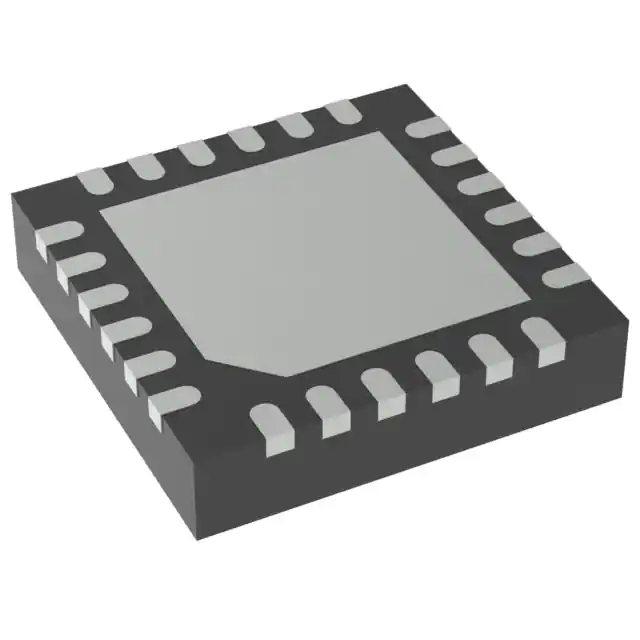


 工商网监
湘ICP备2023018690号
工商网监
湘ICP备2023018690号
