Sample &
Buy
Product
Folder
Support &
Community
Tools &
Software
Technical
Documents
Reference
Design
TPS40180
SLVS753C – FEBRUARY 2007 – REVISED NOVEMBER 2016
TPS40180 Single Phase Stackable Controller
1 Features
3 Description
•
The TPS40180 is a stackable single-phase
synchronous buck controller. Stacking allows a
modular power supply design where multiple modules
can be connected in parallel to achieve higher power
capability. Stacked modules can be configured at the
same switching frequency with interleaved phase shift
to reduce input and output ripple current. Stacked
modules can also be configured to generate separate
output rails at the same time as different phase shift
to reduce input ripple current.
1
•
•
•
•
•
•
•
•
•
•
•
Stackable to 8 Phases, Multiple Controllers Can
Occupy Any Phase
2-V to 40-V Power Stage Operation Range
eTrim™ in System Reference Voltage Trim to
Tighten Overall Output Voltage Tolerance,
Reference is Better Than 0.75% Untrimmed
VDD From 4.5 V to 15 V, With Internal 5-V
Regulator
Supports Output Voltage From 0.7 V to 5.8 V
Supports Prebiased Outputs
10-µA Shutdown Current
Programmable Switching Frequency up to 1-MHz
per Phase
Current Feedback Control With Forced Current
Sharing (Patents Pending)
Resistive Divider Sets Input Undervoltage Lockout
and Hysteresis
True Remote Sensing Differential Amplifier
Resistive or Inductor’s DCR Current Sensing
The TPS40180 is optimized for low-output voltage
(from 0.7-V to 5.8-V), high-output current applications
powered from a 2-V to 40-V supply.
With eTrim™, the TPS40180 gives the user the
capability to trim the reference voltage on the device
to compensate for external component tolerances,
tightening the overall system accuracy and allowing
tighter specifications for output voltage of the
converter.
Device Information(1)
PART NUMBER
TPS40180
2 Applications
•
•
•
•
•
PACKAGE
BODY SIZE (NOM)
VQFN (24)
4.00 mm × 4.00 mm
(1) For all available packages, see the orderable addendum at
the end of the data sheet.
Graphic Cards
Servers
Networking Equipment
Telecommunications Equipment
Distributed DC Power Systems
Typical Application
24
23
22
21
20
19
COMP CS- CS+ PSELPGOOD CLKIO
1
FB
BOOT 18
2
DIFFO
HDRV 17
3
VOUT
4
GSNS
5
VSH
6
ILIM
VIN(+)
VIN(-)
VOUT(+)
SW 16
TS40180
PVCC 15
LDRV 14
SS
7
VOUT(-)
PGND 13
RT GND BP5 UVLO VDD
8
9
10
11
12
Copyright © 2016, Texas Instruments Incorporated
1
An IMPORTANT NOTICE at the end of this data sheet addresses availability, warranty, changes, use in safety-critical applications,
intellectual property matters and other important disclaimers. PRODUCTION DATA.
�TPS40180
SLVS753C – FEBRUARY 2007 – REVISED NOVEMBER 2016
www.ti.com
Table of Contents
1
2
3
4
5
6
7
Features ..................................................................
Applications ...........................................................
Description .............................................................
Revision History.....................................................
Pin Configuration and Functions .........................
Specifications.........................................................
1
1
1
2
3
5
6.1
6.2
6.3
6.4
6.5
6.6
5
5
5
5
6
9
Absolute Maximum Ratings ......................................
ESD Ratings..............................................................
Recommended Operating Conditions.......................
Thermal Information ..................................................
Electrical Characteristics...........................................
Typical Characteristics ..............................................
Detailed Description ............................................ 13
7.1
7.2
7.3
7.4
Overview .................................................................
Functional Block Diagram .......................................
Feature Description.................................................
Device Functional Modes........................................
13
14
15
26
7.5 Programming........................................................... 26
8
Application and Implementation ........................ 30
8.1 Application Information............................................ 30
8.2 Typical Applications ................................................ 30
9 Power Supply Recommendations...................... 44
10 Layout................................................................... 44
10.1 Layout Guidelines ................................................. 44
10.2 Layout Example .................................................... 45
11 Device and Documentation Support ................. 47
11.1
11.2
11.3
11.4
11.5
11.6
Device Support......................................................
Receiving Notification of Documentation Updates
Community Resources..........................................
Trademarks ...........................................................
Electrostatic Discharge Caution ............................
Glossary ................................................................
47
48
48
48
48
48
12 Mechanical, Packaging, and Orderable
Information ........................................................... 48
4 Revision History
Changes from Revision B (November 2007) to Revision C
•
2
Page
Added Feature Description section, Device Functional Modes, Application and Implementation section, Power
Supply Recommendations section, Layout section, Device and Documentation Support section, and Mechanical,
Packaging, and Orderable Information section ...................................................................................................................... 1
Submit Documentation Feedback
Copyright © 2007–2016, Texas Instruments Incorporated
Product Folder Links: TPS40180
�TPS40180
www.ti.com
SLVS753C – FEBRUARY 2007 – REVISED NOVEMBER 2016
5 Pin Configuration and Functions
COMP
CS±
CS+
PSEL
PGOOD
CLKIO
24
23
22
21
20
19
RGE Package
24-Pin VQFN
Top View
GSNS
4
15
PVCC
VSH
5
14
LDRV
ILIM
6
13
PGND
12
SW
VDD
16
11
3
UVLO
VOUT
10
HDRV
BP5
17
9
2
GND
DIFFO
8
BOOT
RT
18
7
1
SS
FB
Not to scale
Pin Functions
PIN
NO.
NAME
I/O
DESCRIPTION
1
FB
I
Inverting input to the internal error amplifier. Normally this pin is at the reference voltage of 700 mV.
2
DIFFO
O
Output of the remote sense amplifier. Amplifier is fixed gain of 1 differential mode and is used for
output voltage sensing at the load to eliminate distribution drops.
3
VOUT
I
Positive input to the remote sense amplifier. Amplifier is fixed gain of 1 differential mode and is used
for output voltage sensing at the load to eliminate distribution drops.
4
GSNS
I
Negative input to the remote sense amplifier. Amplifier is fixed gain of 1 differential mode and is
used for output voltage sensing at the load to eliminate distribution drops.
5
VSH
I/O
6
ILIM
Pin is either an input or an output. If the chip is configured as a voltage loop master the valley
voltage is output on this pin and is distributed to the slave devices. If configured as a voltage loop
slave, the master VSH pin is connected here and the device uses the master valley voltage
reference to improve current sharing.
I
Programs the overcurrent limit of the device. Connecting a resistor from this pin to VSH and another
to VOUT on the voltage loop master sets a voltage above VSH. COMP is not allowed to exceed this
voltage. If the load current requirements force COMP to this level for seven clock cycles, an
overcurrent event is declared, and the system shuts down and enter a hiccup fault recovery mode.
The controller attempts to restart after a time period given by seven soft-start cycles.
7
SS
I
Soft-start input. This pin determines the startup ramp time for the converter as well as overcurrent
and other fault recovery timing. The voltage at this pin is applied as a reference to the error
amplifier. While this voltage is below the precision 700 mV reference, it acts as the dominant
reference to the error amp providing a closed loop startup. After it rises above the 700 mV precision
reference, the 700 mV precision reference dominates and the output regulates at the programmed
level. In case of an overcurrent event, the converter attempts to restart after a period of time defined
by seven soft-start cycles. Additionally this pin is used to configure the chip as a voltage loop
master or slave. If the pin is tied to VDD or PVCC at power up, the device is in voltage loop slave
mode. Otherwise, the device is a voltage loop master.
8
RT
I
Frequency programming pin. Connecting a resistor from this pin to GND sets the switching
frequency of the device. If this pin is connected to VDD or PVCC, the device is a clock slave and
gets its time base from CLKIO of the clock master device. Phase addressing is done on PSEL.
Submit Documentation Feedback
Copyright © 2007–2016, Texas Instruments Incorporated
Product Folder Links: TPS40180
3
�TPS40180
SLVS753C – FEBRUARY 2007 – REVISED NOVEMBER 2016
www.ti.com
Pin Functions (continued)
PIN
NO.
NAME
I/O
DESCRIPTION
9
GND
—
Signal level ground connection for the device. All low level signals at the device should be
referenced to this pin. No power level current should be allowed to flow through the GND pin copper
areas on the board. Connect to the thermal pad area, and from there to the PGND copper area.
10
BP5
I
Electrically quiet 5-V supply for the internal circuitry inside the device. If VDD is above 5 V, connect
a 20-Ω resistor from PVCC to this pin and a 100-nF capacitor from this pin to GND. For VDD at 5 V,
this pin can be tied directly to VDD or through a 20-Ω resistor with a 100-nF decoupling capacitor to
reduce internal noise.
11
UVLO
I
UVLO input for the device. A resistor divider from VDD sets the turn on voltage for the device.
Below this voltage, the device is in a low quiescent current state. Pulling this pin to ground shuts
down the device, and is used as a system shutdown method.
12
VDD
I
Power input for the LDO on the device.
13
PGND
—
Common connection for the power circuits on the device. This pin should be electrically close to the
source of the FET connected to LDRV. Connected to GND only at the thermal pad for best results.
14
LDRV
O
Gate drive output for the low-side or rectifier FET.
15
PVCC
O
Output of the on board LDO. This is the power input for the drivers and bootstrap circuit. The 5.3-V
output on this pin is used for external circuitry as long as the total current required to drive the gates
of the switching FETs and external loads is less than 50 mA. Connect a 1-µF capacitor from this pin
to GND.
16
SW
O
This pin is connected to the source of the high-side or switch FET and is the return path for the
floating high-side driver.
17
HDRV
O
Gate drive output for the high-side FET. High-side FET turn-on time must not be greater than
minimum on-time. See electrical characteristics table for the minimum on time of the pulse width
modulator.
18
BOOT
I
Bootstrap pin for the high-side driver. A 100-nF capacitor is connected from this pin to SW and
provides power to the high-side driver when the high-side FET is turned on.
19
CLKIO
I/O
Clock and phase timing output while the device is configured as a clock master. In clock slave
mode, the master CLKIO pin is connected to the slave CLKIO pin to provide time base information
to the slave.
20
PGOOD
O
Power good output. This open drain output pulls low when the device is in any state other than in
normal regulation. Active soft start, UVLO, overcurrent, undervoltage, overvoltage or
overtemperature warning (115°C junction) causes this output to pull low.
21
PSEL
I
Phase select pin. For a clock master, a resistor from this pin to GND determines the CLKIO output.
When configured as a clock slave, a resistor from the pin to GND selects the phase relationship that
the slave has with the master. Allowing this pin to float causes the slave to drop off line to shed the
phase when current demands are light for improved overall efficiency. See Detailed Description for
more details.
22
CS+
I
Positive input to the current sense amplifier.
23
CS–
I
Negative input to the current sense amplifier.
24
COMP
O
Output of the error amplifier.
4
Submit Documentation Feedback
Copyright © 2007–2016, Texas Instruments Incorporated
Product Folder Links: TPS40180
�TPS40180
www.ti.com
SLVS753C – FEBRUARY 2007 – REVISED NOVEMBER 2016
6 Specifications
6.1 Absolute Maximum Ratings
over operating free-air temperature range (unless otherwise noted) (1)
Input voltage, VI
MIN
MAX
VDD, UVLO, RT, SS
–0.3
16
FB, VOUT, GSNS, VSH, ILIM, BP5, PSEL, CS+, CS–, VS+, VS–
–0.3
6
BOOT – HDRV
–0.3
6
–1
44
SW, HDRV
Output voltage, VO
V
–5
44
DIFFO, LDRV, PVCC, CLKIO, PGOOD, COMP
–0.3
6
PGOOD (eTrim™ usage only)
–0.3
22
Operating junction temperature, TJ
–40
150
°C
Storage temperature, Tstg
–55
150
°C
(1)
SW, HDRV, transient ( 1.98 V,
V(VDD) – V(VOUT) > 2 V
2
V(VOUT) – V(GSNS) = 5.8 V,
V(DIFFO) > 5.6 V,
V(VDD) – V(VOUT) > 1 V
1
V(VOUT) – V(GSNS) = 2 V,
V(DIFFO) > 2.02 V
2
mA
5
8
Inverting, DIFFO to GSNS
60
Noninverting, OUT to GND
60
mA
MHz
kΩ
PSEL PIN
IISEL
Bias current
VMNCLK
VM8PH
21.5
23.5
25.5
0
0
0.5
8 phase CLKIO
0.5
0.7
0.9
6 phase CLKIO
0.9
No output on CLKIO
Master mode
VM6PH
3.4
µA
V
VSSTDBY
Slave mode, standby state
VS45
Clock slave mode,
45° phase slot (1)
V
8 phase CLKIO
0
0
0.2
V
VS90
Clock slave mode,
90° phase slot (1)
8 phase CLKIO
0.2
0.35
0.5
V
VS135
Clock slave mode,
135° phase slot (1)
8 phase CLKIO
0.5
0.7
0.9
V
VS180
Clock slave mode,
180° phase slot (1)
8 phase CLKIO
0.9
1.1
1.3
V
VS225
Clock slave mode,
225° phase slot (1)
8 phase CLKIO
1.3
1.6
1.9
V
VS270
Clock slave mode,
270° phase slot (1)
8 phase CLKIO
1.9
2.25
2.6
V
VS315
Clock slave mode,
315° phase slot (1)
8 phase CLKIO
2.6
3
3.4
V
VS0
Clock slave mode,
0 phase slot (1)
6 phase CLKIO
1.9
2.25
2.6
V
VS60
Clock slave mode,
60° phase slot (1)
6 phase CLKIO
0
0
0.2
V
VS120
Clock slave mode,
120° phase slot (1)
6 phase CLKIO
0.2
0.35
0.5
V
VS180
Clock slave mode,
180° phase slot (1)
6 phase CLKIO
0.5
0.7
0.9
V
Submit Documentation Feedback
Copyright © 2007–2016, Texas Instruments Incorporated
Product Folder Links: TPS40180
7
�TPS40180
SLVS753C – FEBRUARY 2007 – REVISED NOVEMBER 2016
www.ti.com
Electrical Characteristics (continued)
VVDD = 12 V, VBP5 = 15 V, VPVCC = 5 V, –40°C ≤ TJ ≤ 85°C (unless otherwise noted)
PARAMETER
TEST CONDITIONS
MIN
TYP
MAX
UNIT
VS240
Clock slave mode,
240° phase slot (1)
6 phase CLKIO
0.9
1.1
1.3
V
VS300
Clock slave mode,
300° phase slot (1)
6 phase CLKIO
1.3
1.6
1.9
V
GATE DRIVERS
RHDRV(on)
HDRV pull up resistance
VBOOT = 5 V, V(SW) = 0 V,
IHDRV = 100 mA
1
2
3
Ω
RHDRV(off)
HDRV pull down resistance
VBOOT = 5 V, V(SW) = 0 V,
IHDRV = 100 mA
0.5
1
2
Ω
RLDRV(on)
LDRV pull up resistance
VPVCC = 5 V, ILDRV = 100 mA
1
2
3.5
Ω
RLDRV(off)
LDRV pull down resistance
VPVCC = 5 V, ILDRV = 100 mA
0.3
0.75
1.5
Ω
(1)
tHDRV(r)
HDRV rise time
CLOAD = 3.3 nF
25
75
ns
tHDRV(f)
HDRV fall time (1)
CLOAD = 3.3 nF
25
75
ns
tLDRV(r)
LDRV rise time (1)
CLOAD = 3.3 nF
25
75
ns
CLOAD = 3.3 nF
10
60
ns
tLDRV(f)
LDRV fall time
(1)
POWER GOOD
VFBPG_H
Power good high FB voltage
threshold
764
787
798
mV
VFBPG_L
Power good low FB voltage
threshold
591
611
626
mV
VFBPG(hyst)
Power good threshold hysteresis
60
mV
30
(1)
TPGDLY
Power good delay time
VPGL
Power good low level output voltage
IPG = 2 mA
10
IPGLK
Power good leakage current
VPG = 5 V
0.35
µs
0.4
1
V
µA
OVERVOLTAGE AND UNDERVOLTAGE
VFB_U
FB pin under voltage threshold
565
580
595
mV
VFB_O
FB pin over voltage threshold
792
810
828
mV
126
135
144
°C
THERMAL SHUTDOWN
TTSD
Shutdown temperature (1)
TTSD(hyst)
Hysteresis (1)
TWRN
Warning temperature (1)
TWR(hyst)
8
Hysteresis
40
106
(1)
115
10
Submit Documentation Feedback
°C
124
°C
°C
Copyright © 2007–2016, Texas Instruments Incorporated
Product Folder Links: TPS40180
�TPS40180
www.ti.com
SLVS753C – FEBRUARY 2007 – REVISED NOVEMBER 2016
6.6 Typical Characteristics
0.6
VISOFST - Current Sense Offset Voltage - mV
6
IVDD - Input Current - mA
5
4
3
2
1
0
-50
-30
-10
10
30
50
70
90
0.4
0.2
0
-0.2
-0.4
-0.6
-0.8
-50
110
-30
30 mV
0
60 mV
-0.5
10
30
50
70
90
110
22.5
22.0
21.5
21.0
-30
-10
10
30
50
70
90
110
TJ - Junction Temperature - °C
TJ - Junction Temperature - °C
Figure 3. Relative Current Sense Gain
vs Junction Temperature
Figure 4. Current Limit vs Junction Temperature
1.810
VVSH - Current Share Reference Voltage - V
245
VBP5UVH - UVLO Hysteresis - mV
90
23.0
20.0
-50
110
250
240
235
230
225
220
215
210
205
200
-50
70
20.5
5 mV
-10
50
23.5
0.5
-30
30
24.0
CS+ - CS60 mV
30 mV
5 mV
-1.0
-50
10
Figure 2. Current Sense Amplifier Offset Voltage
vs Junction Temperature
IILIM - Current Limit Current - mA
GCS - Current Sense Gain - V/V%
Figure 1. Input Shutdown Current vs Junction Temperature
1.0
-10
TJ - Junction Temperature - °C
TJ - Junction Temperature - °C
-30
-10
10
30
50
70
90
110
1.805
1.800
1.795
1.790
-50
-30
-10
10
30
50
70
90
110
TJ - Junction Temperature - °C
TJ - Junction Temperature - °C
Figure 5. UVLO Hysteresis vs Junction Temperature
Figure 6. Current Share RE Voltage
vs Junction Temperature
Submit Documentation Feedback
Copyright © 2007–2016, Texas Instruments Incorporated
Product Folder Links: TPS40180
9
�TPS40180
SLVS753C – FEBRUARY 2007 – REVISED NOVEMBER 2016
www.ti.com
Typical Characteristics (continued)
GRVS - Remote Voltage Sense Amplifier Gain - V/V
ISSx - Soft-Start Charge Current - mA
17
15
13
ISS2
11
ISS1
9
7
5
-50
-30
-10
10
30
50
70
90
110
0.05
0.04
0.03
0.02
0.01
0
-0.01
-0.02
-0.03
-0.04
-0.05
-50
10
30
50
70
90
110
Figure 7. Soft-Start Charge Current vs Junction
Temperature
Figure 8. Remote Voltage Sense Amplifier
vs Junction Temperature
900
1.6
VFBPG - Power Good FB Threshold Voltage - V
RHDRV(on)
RHDRV(off)
RLDRV(on)
RLDRV(off)
1.8
RxDRV - Driver Resistance - W
-10
TJ - Junction Temperature - °C
2.0
1.4
1.2
1.0
0.8
0.6
0.4
0.2
0
-50
-30
-10
10
30
50
70
90
850
800
750
High
700
Low
650
600
550
500
-50
110
-30
-10
10
30
50
70
90
110
TJ - Junction Temperature - °C
Figure 9. Driver Resistance vs Junction Temperature
Figure 10. Power Good Threshold Voltage
vs Junction Temperature
0.05
VFBPG(hyst) - Power Good FB Hysteresis - mV
GRVS - Remote Voltage Sense Amplifier Gain - V/V
TJ - Junction Temperature - °C
0.04
0.03
0.02
0.01
0
-0.01
-0.02
-0.03
-0.04
-0.05
-50
10
-30
TJ - Junction Temperature - °C
-30
-10
10
30
50
70
90
110
50
40
30
20
10
0
-50
-30
-10
10
30
50
70
90
110
TJ - Junction Temperature - °C
TJ - Junction Temperature - °C
Figure 11. Power Good Low Threshold Voltage
vs Junction Temperature
Figure 12. Power Good FB Hysteresis
vs Junction Temperature
Submit Documentation Feedback
Copyright © 2007–2016, Texas Instruments Incorporated
Product Folder Links: TPS40180
�TPS40180
www.ti.com
SLVS753C – FEBRUARY 2007 – REVISED NOVEMBER 2016
Typical Characteristics (continued)
980
VUVLO - Undervoltage Lockout Threshold - V
VVFB_x - Feedback Voltage Thresholds - mV
900
850
800
750
Overvoltage
700
Undervoltage
650
600
550
500
450
400
-50
-30
-10
10
30
50
70
90
960
940
920
900
880
860
840
820
-50
110
-30
-10
10
30
50
70
90
110
TJ - Junction Temperature - °C
TJ - Junction Temperature - °C
Figure 13. Undervoltage and Overvoltage Threshold
vs Junction Temperature
Figure 14. UVLO Enable Threshold vs Junction Temperature
2.025
12.0
VUVLO - UVLO PWM Enable Threshold - V
11.8
IUVLO - Hysteresis Current - mA
11.6
11.4
11.2
11.0
10.8
10.6
10.4
10.2
10.0
-50
-30
-10
10
30
50
70
90
110
2.020
2.015
Enable
2.010
2.005
2.000
Disable
1.995
1.990
1.985
-50
-30
0.30
50
0.25
45
0.20
40
IIB - Feedback Bias Current - nA
VFB - Relative Feedback Voltage Change - %
10
30
50
70
90
110
Figure 16. UVLO PWM Enable Threshold Voltage
vs Junction Temperature
Figure 15. UVLO Hysteresis Current
vs Junction Temperature
0.15
0.10
0.05
0
-0.05
-0.10
-0.15
-0.20
-50
-10
TJ - Junction Temperature - °C
TJ - Junction Temperature - °C
35
30
25
20
15
10
5
-30
-10
10
30
50
70
90
110
0
-50
-30
-10
10
30
50
70
90
110
TJ - Junction Temperature - °C
TJ - Junction Temperature - °C
Figure 17. Relative Feedback Reference Voltage Change
vs Junction Temperature
Figure 18. Feedback Bias Current vs Junction Temperature
Submit Documentation Feedback
Copyright © 2007–2016, Texas Instruments Incorporated
Product Folder Links: TPS40180
11
�TPS40180
SLVS753C – FEBRUARY 2007 – REVISED NOVEMBER 2016
www.ti.com
Typical Characteristics (continued)
5
fOSC - Relative Oscillator Frequency - %
4
3
3
1
0
-1
-2
-3
-4
-5
-50
-30
-10
10
30
50
70
90
110
TJ - Junction Temperature - °C
Figure 19. Relative Oscillator Frequency vs Junction Temperature
12
Submit Documentation Feedback
Copyright © 2007–2016, Texas Instruments Incorporated
Product Folder Links: TPS40180
�TPS40180
www.ti.com
SLVS753C – FEBRUARY 2007 – REVISED NOVEMBER 2016
7 Detailed Description
7.1 Overview
The TPS40180 is a versatile single-phase controller that can be used as a building block for a more complex
power system, or as a stand-alone power supply controller. In either system, the TPS40180 provides an
excellent power conversion solution and supports such features as prebias start-up, intelligent fault handling
capability with graceful shutdown and restart even with multiple modules sharing a common load. Remote load
voltage sense for improved load regulation where it counts, at the load, thermal shutdown, remote enable and
power good indication features help solve the problems faced by the power supply designer. To ease application
to a specific task, there are several user programmable features including closed loop soft-start time, operating
frequency and current limit level.
More complex power solutions are readily supported by the TPS40180. The device can be configured to run in a
master/slave configuration where a master can control several slaves. Several options are possible including a
single output multiple phase supply sharing phase timing information to reduce input and output ripple, a multiple
output supply that shares phase switching timing information to reduce input ripple currents, and a combination
approach that has multiple outputs sharing phase information where each output can use multiple phases. Phase
information in all cases comes from a single device designated the clock master. Current sharing information is
passed from the device designated voltage loop master for each output to the slaves for that particular output rail
by connecting the COMP pin of the master to the COMP pin of the slaves. The clock master is also the voltage
loop master in one of the rails of a multiple output supply; whereas, the other rails are controlled by a voltage
loop master that is a clock slave to the single clock master device.
Submit Documentation Feedback
Copyright © 2007–2016, Texas Instruments Incorporated
Product Folder Links: TPS40180
13
�TPS40180
SLVS753C – FEBRUARY 2007 – REVISED NOVEMBER 2016
www.ti.com
7.2 Functional Block Diagram
VO
VSH
RT
CLKIO
5
8
19
PSEL
21
3
+
GSNS
4
DIFFO
2
CLK
Oscillator
17 HDRV
UVLO
Error Amplifier
FB
18 BOOT
Anti-Cross
Conduction
+
1
700 mV
S
+
-
SS
+
16 SW
PWM
Comparator
PVCC
14 LDRV
COMP 24
22
CS-
23
Current Sense
X12.5
Overvoltage/
Undervoltage
Control
VSLAVE
CS+
+
13 PGND
CLK
BP5
23.5mA
BP5
ILIM
Fault Control
and Soft-Start
6
VDD
7.5mA
FAULT
10 BP5
20 PGOOD
7.5mA
PGOOD
Controller
SS
7
BP5
12mA
140°C
2V
+
UVLO 11
UVLO
110°C
Junction
Temperature
12 VDD
5-V
Regulator
0.9 V
+
15 PVCC
9
UDG-07036
GND
Copyright © 2016, Texas Instruments Incorporated
14
Submit Documentation Feedback
Copyright © 2007–2016, Texas Instruments Incorporated
Product Folder Links: TPS40180
�TPS40180
www.ti.com
SLVS753C – FEBRUARY 2007 – REVISED NOVEMBER 2016
7.3 Feature Description
7.3.1 Current Sensing and Overcurrent Detection
The TPS40180 uses the current sensing architecture shown in Figure 20.
IOUT
CS+
CS-
22
23
TPS40180
VC
+
CS gain = 12.5
+
COMP
24
+
-
E/A
+
Ve
S
+
PWM
Ramp
VSH
5
23.5mA
R1
ILIM
0.5 V
+
+
1.8 V
S
+
0V
+
6
R2
Overcurrent
VOUT
Copyright © 2016, Texas Instruments Incorporated
Figure 20. Current Sense Architecture
The sense resistor can either be a resistor between the inductor and the output capacitor(s) or an R-C filter
across the inductor.
Overcurrent protection for the TPS40180 is set by connecting a resistor from the ILIM pin to the VSH pin. A
current source of 23.5 µA out of the ILIM pin sets a voltage level on the ILIM pin and the COMP pin is not
allowed to rise above this level. Since the device uses current mode control and COMP cannot rise above this
level, an effective maximum output current is defined. The second resistor on the ILIM pin, R2, is optional and if
used is connected to the output voltage. This resistor provides compensation of the overcurrent level for changes
in output voltage, such as would be seen at start-up. If not used, the overcurrent threshold level is higher at
output voltages lower than the designed target.
The output current, flows through the inductor resistance and develops a voltage, VC across it, representative of
the output current. This resistance voltage is extracted from the total inductor voltage by the R-C network placed
across the inductor. This voltage is amplified with a gain of 12.5 and then subtracted from the error amplifier
output, COMP, to generate the Ve voltage. The Ve signal is compared to the slope-compensation RAMP signal
to generate the PWM signal that is used to control the FET drivers. As the output current is increased, the
amplified VC causes the Ve signal to decrease. In order to maintain the proper duty cycle, the COMP signal must
increase. Therefore, the magnitude of the COMP signal contains the output current information as shown in
Equation 1 through Equation 3.
COMP = Ve + (I pk ´ RL ) ´ 12.5
(1)
æ (V - VOUT ) ö æ VOUT
I RIPPLE = ç IN
÷´ç
L
è
ø è VIN
æ I RIPPLE
I PK = ç
ç 2
è
ö æ 1 ö
÷
÷´ç
ø è ƒSW ø
(2)
ö
÷÷ + IOUT
ø
(3)
In order to satisfy the input-output voltage relationship, Equation 4 must hold.
Submit Documentation Feedback
Copyright © 2007–2016, Texas Instruments Incorporated
Product Folder Links: TPS40180
15
�TPS40180
SLVS753C – FEBRUARY 2007 – REVISED NOVEMBER 2016
www.ti.com
Feature Description (continued)
Ve = VRMP ´
VOUT
+ VVSH
VIN
(4)
Combining Equation 1 and Equation 4 and solving for the COMP voltage gives Equation 5.
æV
COMP = VRMP ´ ç OUT
è VIN
ö
÷ + VVSH + (I PK ´ RL ) ´ 12.5
ø
(5)
Since COMP and ILIM are of equal voltage when at the current limit condition, setting ILIM to the expected
COMP voltage at maximum current is how the current limit threshold is set. To calculate the resistors R1 and R2
from Figure 20, use Equation 6 through Equation 9.
æV
ö
a = ç RMP ÷
è VIN ø
(6)
æ V
ö
b = RL ´ 12.5 ´ I PK + ç RMP ÷
ç (2 ´ Nph ) ÷
è
ø
b + a ´ VVSH
R1 =
(1 - a ) ´ IILIM
(7)
(8)
a + b ´ VVSH
R2 =
a ´ IILIM
where (for Equation 1 through Equation 9)
•
•
•
•
•
•
•
•
•
•
•
•
COMP is the voltage on the COMP pin
VRMP is the ramp amplitude, 500 mV
VOUT is the output voltage of the converter
IOUT is the dc output current of the converter
VIN is the input voltage of the converter
VVSH is the valley voltage of the ramp, 1.8 V
IPK is the peak current in the inductor
RL is the DC resistance of the inductor
L is the inductance of the inductor
12.5 is the gain of the current sense amplifier network inside the device
Nph is the number of phase that the master clock is set to, either 6 or 8
IILIM is the bias current out of the ILIM pin, 23.5 µA typical
(9)
The TPS40180 architecture inherently allows multiple modules to start simultaneously into a load without
problems with overcurrent tripping. The reason this is the case is the master device in a group of devices
configured as a multiphase power supply is the only device that retains overcurrent control. The slave devices do
not have the ability to initiate an overcurrent event but rely on the master to handle this function. For this reason,
when setting the overcurrent threshold for a multiple converter system, the previous equations should be used to
set the threshold on a per-converter basis. For example, if four converters are being used to generate a supply
that has a 60-A current limit, the current limit to use for calculating the resistors would be 15 A.
NOTE
The above equations indicate that the overcurrent threshold is dependent on input voltage.
Consequently, as the input voltage increases, the overcurrent threshold also rises.
7.3.2 Hiccup Fault Recovery
To reduce the input current and component dissipation during on overcurrent event, a hiccup mode is
implemented. Hiccup mode refers to a sequence of 7 soft-start cycles where no MOSFET switching occurs, and
then a re-start is attempted. If the fault has cleared, the re-start results in returning to normal operation and
regulation. This is shown in Figure 21.
16
Submit Documentation Feedback
Copyright © 2007–2016, Texas Instruments Incorporated
Product Folder Links: TPS40180
�TPS40180
www.ti.com
SLVS753C – FEBRUARY 2007 – REVISED NOVEMBER 2016
Feature Description (continued)
VVDD
SS
1.5 V
(A)
0.5 V
GND
VIN
(B)
SW NODE
GND
VOUT, REG
(C)
VOUT
GND
ILIM
(D)
COMP
t0 t1 t2
t3
Figure 21. Hiccup Recovery From Faults
Normal operation is occurring between t0 and t1 as shown by VOUT at the regulated voltage, (C) and normal
switching on the SW NODE (B) and COMP at its nominal level, (D). At t1, an overcurrent load is experienced.
The increased current forces COMP to increase to the ILIM level as shown in (D). If the COMP voltage is above
the ILIM voltage for 7 switching cycles, the controller enters a hiccup mode at t2. During this time the controller is
not switching and the power MOSFETs are turned off. The SS pin goes through 7 cycles of charging and
discharging the soft-start capacitor. At the end of the 7 cycles the controller attempts another normal re-start. If
the fault has been cleared, the output voltage comes up to the regulation level as shown at time t3. If the fault
has not cleared, the COMP voltage again rises above the ILIM voltage and a fresh hiccup cycle starts. This
condition may continue indefinitely.
The prebias circuitry is reset at this time and the restart does not discharge an output prebias condition if it
exists.
7.3.3 Selecting Current Sense Network Components
Some consideration must be given to selecting the components that are used to sense current in the converter. If
an R-C filter across the inductor is used, the R-C time constant should match the natural time constant of the
inductor. Equation 10 and Figure 22 describe the relationship.
æ L ö
RCS ´ CCS = ç
÷
è RL ø
(10)
Inductor
L
RL
CCS
RCS
+
VC
_
Figure 22. Current Sense Network
Submit Documentation Feedback
Copyright © 2007–2016, Texas Instruments Incorporated
Product Folder Links: TPS40180
17
�TPS40180
SLVS753C – FEBRUARY 2007 – REVISED NOVEMBER 2016
www.ti.com
Feature Description (continued)
The amplitude of the VC voltage must also be considered. If the VC voltage is expected to rise above 60 mV at
the desired overcurrent threshold, an attenuator should be used to keep the voltage to a maximum of 60 mV. To
implement the divider, place a resistor in parallel with CCS. The time constant of the whole network should remain
the same as the L/R time constant of the inductor.
High-ripple current applications can also cause problems under certain conditions. When the sensing network is
matched to the inductor, the ripple voltage on the capacitor CCS is the same as the ripple voltage produced on
the effective inductor resistance. If this ripple component is too great, subharmonic instability can result and the
PWM exhibits excessive jitter or give a long pulse, short pulse type of output. To minimize this effect, the slope of
the signal presented to the current sense amplifier must be less than a maximum value. This places a minimum
limit on what the inductor L/R time constant can be for a given application as shown in Equation 11. If the chosen
inductor and other application parameters fall outside these recommendations, it is necessary to attenuate the
current feedback signal with an extra resistor.
æ L ö GCS(max) ´ (VIN + (2 ´ VOUT ))
ç
÷>
fSW
è RL ø
where
•
•
•
•
•
•
L is the inductance in H
RL is the equivalent series resistance of the inductor in Ω
GCS(max) is the maximum gain of the current sense amplifier, 13.75
VIN is the input voltage in V
VOUT is the output voltage in V
fSW is the switching frequency in Hz
(11)
7.3.4 PGOOD Functionality
PGOOD functions as a normal, open-drain power good output on an device configured as a master. This is an
open-drain signal and pulls low when any condition exists that would indicate that the output of the supply might
be out of regulation. These conditions include:
• FB pin more that ±15% from nominal
• Soft start is active
• A UVLO condition exists for the TPS40180
• The TPS40180 has detected a short-circuit condition
• The TPS40180 die is over warning temperature threshold (115°C)
If the device is configured as a voltage loop slave, PGOOD pulls low the following conditions only:
• A UVLO condition exists for the TPS40180
• The TPS40180 die is over warning temperature threshold (115°C)
Note that when there is no power to the device, PGOOD is not able to pull close to GND if an auxiliary supply is
used for the power good indication.
7.3.5 Output Overvoltage and Undervoltage Protection
If the output voltage is sensed to be too low, the TPS40180 turns off the power FETs, and initiates a hiccup
restart sequence just as if a fault condition had occurred. The sensing of the output voltage is done using the FB
pin and the undervoltage threshold voltage for the FB pin is 580-mV typical. The prebias circuitry is reset at this
time and the restart does not discharge an output prebias condition if it exists.
The TPS40180 also includes an output overvoltage protection mechanism. This mechanism is designed to turn
on the low-side FET when the FB pin voltages exceeds the overvoltage protection threshold of 810-mV (typical).
The high-side FET turns off and the low-side FET turns on and stays on until the voltage on the FB drops below
the undervoltage threshold. At this point, the controller enters a hiccup recovery cycle as in the undervoltage
case. The output overvoltage protection scheme is active at all times. If at any time when the controller is
enabled, the FB pin voltage exceeds the overvoltage threshold, the low-side FET turns on until the FB pin
voltage falls below the undervoltage threshold.
18
Submit Documentation Feedback
Copyright © 2007–2016, Texas Instruments Incorporated
Product Folder Links: TPS40180
�TPS40180
www.ti.com
SLVS753C – FEBRUARY 2007 – REVISED NOVEMBER 2016
Feature Description (continued)
7.3.6 Overtemperature Protection
When the TPS40180 die temperature exceeds 115°C, the PG pin is pulled low as a warning that temperatures
are becoming excessive. Systems can act on this indication as appropriate.
The TPS40180 shuts down if the die temperature is sensed to be more than 135°C. The die must cool to less
than the warning level reset of 105°C before the device restarts. The device restarts automatically after the die
cools to this level.
7.3.7 eTRIM™
The TPS40180 incorporates an innovative new feature that allows the user to trim the reference voltage in
system. This allows the user to tighten overall output tolerances by trimming out errors caused by resistor divider
and other system tolerances. The reference has been designed so that it may be trimmed without affecting
temperature drift so that the user can perform system level trims without worrying about creating a situation
where the reference temperature drift becomes a problem. Trimming in the TPS40180 is done with a small bank
of EEPROM. Changing bit values in this EEPROM causes parameters, like reference voltage, inside the device
to change. Once trim is accomplished, there is no need to trim again, the change is permanent (but can be
overwritten by subsequent trimming operations). The eTrim™ trimming mechanism has been designed so that
the user can only program the reference voltage so that any errors in the programming sequence does not affect
other factory set trims such as current feedback gain for example. This provides a secure environment for the
user to use and eliminates the possibility that other parameters could inadvertently changed.
The adjustment range is ±14 mV from the untrimmed level. The reference is pre-trimmed at the factory to ±0.5%
of nominal so further trim is not necessary unless it is desired to further reduce total system errors. This factory
trim uses the same eTrim™ mechanism that can be used at the system or converter level and changes the same
bits that the user changes if using eTrim™. Consequently, not all of the trim range may be available to make
adjustments in system as the factory trim sets the bits to the value that provides the correct nominal reference
voltage. Typically, the trim has at least 3 steps remaining in any direction to allow for user system level trim.
There are several steps required to use the eTrim™ feature. A typical trim sequence would flow as follows:
1. Power up the system and wait for the system to stabilize in steady state
2. Program the TPS40180 reference trim to a default setting (overwriting factory trim)
3. Measure the system output voltage
4. Calculate a correction factor to be applied to the output voltage
5. Program the EEPROM inside the TPS40180 with the new trim code
6. Measure the new system output voltage
7. Repeat from step 4 if required
The TPS40180 provides 4 trim bits available for user programming. The bits and their effect on the untrimmed
reference value are given in Table 1.
Table 1. eTrim Bit Codes and Effect
eTrim™ REFERENCE BIT CODE
(1)
b3
b2
b1
b0
REFERENCE CHANGE
(mV)
1
0
0
0
+14
1
0
0
1
+12
1
0
1
0
+10
1
0
1
1
+8
1
1
0
0
+6
1
1
0
1
+4
1
1
1
0
+2
1
1
1
1
0 (1)
0
0
0
0
0
0
0
0
1
–2
Default setting
Submit Documentation Feedback
Copyright © 2007–2016, Texas Instruments Incorporated
Product Folder Links: TPS40180
19
�TPS40180
SLVS753C – FEBRUARY 2007 – REVISED NOVEMBER 2016
www.ti.com
Table 1. eTrim Bit Codes and Effect (continued)
eTrim™ REFERENCE BIT CODE
b3
b2
b1
b0
REFERENCE CHANGE
(mV)
0
0
1
0
–4
0
0
1
1
–6
0
1
0
0
–8
0
1
0
1
–10
0
1
1
0
–12
0
1
1
1
–14
The process of writing to the on chip trim EEPROM is as follows. With power applied to the system and the
system in steady state:
1. Force the input voltage to the device, VVDD, to a level of 7 V (this eases stresses on the UVLO pin).
2. Raise the UVLO pin to a level 2 V above VVDD and PGOOD to 20 V
3. Apply a pulse of VVDD + 4 V for a minimum of 10 µs to UVLO
4. Bring UVLO to VVDD + 2 V for at least 8 µs
5. The UVLO pin is then pulsed to VVDD + 4 V seven times (six address bits and one data bit) for each bit that is
to be written. The pulse period is typically 1 µs and the width of the pulse determines whether the pulse is
interpreted as a 1 or as a 0 by the EEPROM circuitry.
6. Data has been placed in a buffer. To finalize the writing, pull PGOOD to 20 V and the UVLO pin to
VVDD + 4 V for at least 15 ms.
Figure 23 shows a typical sequence.
VDD
VVDD
‘0’ programmed to bit 0
‘1’ programmed to bit 1
A5 A4 A3 A2 A1 A0 D
A5 A4 A3 A2 A1 A0 D
VVDD+4 V
VVDD+2 V
UVLO
> 2.5 V
Settle Time
>=15 ms
15 ms write EEPROM
>10ms >8ms 1ms1ms
20 V
PGOOD
Figure 23. eTrim™ EEPROM Programming Sequence
The pulses from VVDD + 2 V to VVDD + 4 V on UVLO are governed by the timing shown in Figure 24.
There are six address bits in the sequence to write to a single EEPROM bit. To write to the eTrim™ accessible
bits, the address sequence must be correct for all six bits or else the write attempt has no effect. To write to
eTrim™ accessible bits the first four address bits must be zero. Anything else is not accepted. Address bits A1
and A0 select which eTrim™ accessible EEPROM bit is written. For example, to write a 1 to bit 3 of the eTrim™
accessible bits, the data pulse sequence would look like Figure 25.
100 ns
A5
A4
A3
A2
A1
A0
0
0
0
0
1
1
D
‘0’
900 ns
1
Figure 25. Write 1 to Bit 3
‘1’
1ms
Figure 24. eTrim™ Bit Pulse Timing
20
Submit Documentation Feedback
Copyright © 2007–2016, Texas Instruments Incorporated
Product Folder Links: TPS40180
�TPS40180
www.ti.com
SLVS753C – FEBRUARY 2007 – REVISED NOVEMBER 2016
As data is clocked into the device, the reference voltage reflects the updates without writing the data buffer to the
actual EEPROM. System measurements can be made after a suitable system dependent settling time has
elapsed after changing the bits in the buffer. When satisfied with the results, the EEPROM may be written by
pulling PGOOD to 20 V and UVLO to VVDD + 4 V for at least 15 ms. For best reliability, the EEPROM should only
be written to by pulling PGOOD to 20 V and UVLO to VVDD + 4 V a maximum of three times during the product
lifetime. This writing only needs to be done once during the entire trimming cycle, after the optimal trim values
are found since data clocked in will affect the output without performing the actual write. Until written, changes
are not permanent and will be lost after power cycling the device.
7.3.8 Connections Between Controllers for Stacking
One of the main benefits of using the TPS40180 is the ability to parallel output power stages to achieve higher
output currents and to scale or stack on controllers as needed. Phasing information is also shared among the
controllers to minimize input ripple and RMS current in the input stage capacitors. Figure 26 shows the
connections among the controller devices and the controller configuration connections to implement a single
output stacked configuration. Up to 7 slave controllers can be connected to the master controller in this manner
with unique phasing for each controller. More than 7 controllers can also be connected as long as some of them
are programmed to operate at the same phase relationship with respect to the master. Not shown are the power
stage portions of the schematics. The outputs of the individual converters inductors are simply connected
together and then to a common output capacitor bank. All other connections would be as for a single device used
as a converter.
In Figure 26, the master controller is configured as a CLK master and as a voltage control loop master (SS and
RT pin connections). The slave controllers are configured as CLK slaves (RT pin tied to PVCC) and as voltage
control loop slaves (SS pin tied to PVCC).
Submit Documentation Feedback
Copyright © 2007–2016, Texas Instruments Incorporated
Product Folder Links: TPS40180
21
�TPS40180
SLVS753C – FEBRUARY 2007 – REVISED NOVEMBER 2016
www.ti.com
TPS40180
Master
2
DIFFO
1
FB
PSEL 21
VDD 15
24 COMP
RT
8
SS
7
19 CLKIO
5
VSH
TPS40180
Slave
10 kW
2
DIFFO
1
FB
24 COMP
PSEL 21
VDD 15
19 CLKIO
RT
8
5
SS
7
VSH
TPS40180
Slave
2
DIFFO
1
FB
24 COMP
PSEL 21
VDD 15
19 CLKIO
RT
8
5
SS
7
VSH
TPS40180
Slave
2
DIFFO
1
FB
24 COMP
PSEL 21
VDD 15
19 CLKIO
RT
8
5
SS
7
VSH
Copyright © 2016, Texas Instruments Incorporated
Figure 26. Single-Output Stacked Configuration
22
Submit Documentation Feedback
Copyright © 2007–2016, Texas Instruments Incorporated
Product Folder Links: TPS40180
�TPS40180
www.ti.com
SLVS753C – FEBRUARY 2007 – REVISED NOVEMBER 2016
The 10-kΩ resistor connected from the CLKIO line to GND is required to ensure that the CLKIO line falls to GND
quickly when the master device is shutdown or powers off. The master CLKIO pin goes to a high impedance
state at these times and if the CLKIO line was high, there is no other active discharge part. The slave controllers
look at the CLKIO line to determine if the system is supposed to be running or not. A level below 0.5 V on CLKIO
is required for this purpose. If the CLKIO line remains high after that master is shut down, the slaves continue to
operate. This is seen as the slave LDRV signal remaining high for a period of time after the master is shut down
and results in output voltage excursions that are not controlled.
NOTE
In any system configured to have a CLK master and CLK slaves, a 10-kΩ resistor
connected from CLKIO to GND is required.
For simplicity of design, the compensation components shown on the master, as well as the components
connected to the RT and SS pins may be present on the slaves. This prevents separate designs being
necessary for master and slave circuits. The RT and SS pins can have jumper option to tie them to VDD to
program an individual device as a slave. These components were omitted in Figure 26.
Selection of the PSEL pin resistors is simple. First determine if the master should generate a CLK signal that is
suitable for 60 or 45 spacing of the phases. Select the appropriate PSEL connection option from Table 3. For the
slaves, determine the desired firing angle for each one and pick the appropriate resistor from either Table 4 or
Table 5 depending on the clock scheme chosen for the master.
Design Note: When used in a master/slave relationship and an overvoltage event occurs, only the control loop
master turns on the low-side FET to pull down the output voltage. This results in the master phase low-side FET
sinking all of the combined maximum current for the slaves. For example, if the per phase current limit is 10 A
and there are 4 phases, the master low-side FET could be required to pass 30 A for a brief time. The master
error amplifier is still active during this time and tries to have the slaves regulate the output voltage. As the
master COMP pin rises to the ILIM point, a fault event is sensed and the converter shuts down, and then initiate
a hiccup restart. Size the master low-side FET to handle the appropriate amount of surge current for 7 clock
cycles of the converter.
A connection diagram for several controllers sharing phase information and synchronized to each other but
having different output voltages is shown in Figure 27. This is similar to the previous example but here the
controllers are all control loop masters (SS not pulled to VDD) and control their own output voltages
independently. One device is configured as a CLK master (RT not tied to VDD) and is the clock generator for the
CLK slaves. Picking the PSEL resistors is the same as before. overcurrent in this configuration depends on
which controller senses the overcurrent event. If one of the CLK slaves experiences a fault, that converter only
shuts down, and enter the hiccup restart mode. If the CLK master controller senses an overcurrent, it stops
sending CLKIO pulses to the slaves, causing them to stop. The master then enters a hiccup recovery mode.
Submit Documentation Feedback
Copyright © 2007–2016, Texas Instruments Incorporated
Product Folder Links: TPS40180
23
�TPS40180
SLVS753C – FEBRUARY 2007 – REVISED NOVEMBER 2016
www.ti.com
TPS40180
CLK Master
2
DIFFO
1
FB
PSEL 21
VDD 15
24 COMP
RT
8
SS
7
19 CLKIO
10 kW
5
VSH
TPS40180
CLK Slave
2
DIFFO
1
FB
PSEL 21
VDD 15
24 COMP
19 CLKIO
5
RT
8
SS
7
VSH
TPS40180
CLK Slave
2
DIFFO
1
FB
PSEL 21
VDD 15
24 COMP
19 CLKIO
5
RT
8
SS
7
VSH
Copyright © 2016, Texas Instruments Incorporated
Figure 27. Phase Share Multiple Output Configuration
Finally, a configuration diagram for multiple multiphase converters is shown in Figure 28. This is just a
combination of the two previous examples and should follow intuitively once those are understood. It is the
example of Figure 26 with a CLK slave but control loop master added to create a second output voltage while
sharing phasing information with the first converter group. A slave has been added to the second control loop
master controller in this case as well creating a grouping of controllers that provide a second output voltage. This
can have a significant impact on the required input filter capacitance if all the converters are located close to one
another.
24
Submit Documentation Feedback
Copyright © 2007–2016, Texas Instruments Incorporated
Product Folder Links: TPS40180
�TPS40180
www.ti.com
SLVS753C – FEBRUARY 2007 – REVISED NOVEMBER 2016
VOUT1
VOUT2
TPS40180
CLK Master
Loop 1 Master
2
DIFFO
1
FB
TPS40180
CLK Slave
Loop 2 Master
PSEL 21
VDD 15
RT
24 COMP
DIFFO
1
FB
SS
TPS40180
Slave
1
FB
24 COMP
RT
8
SS
7
19 CLKIO
7
5
DIFFO
VDD 15
24 COMP
VSH
2
PSEL 21
8
19 CLKIO
5
2
VSH
TPS40180
Slave
10 kW
PSEL 21
VDD 15
2
DIFFO
1
FB
24 COMP
PSEL 21
VDD 15
19 CLKIO
RT
8
19 CLKIO
RT
8
5
SS
7
5
SS
7
VSH
VSH
TPS40180
Slave
2
DIFFO
1
FB
24 COMP
PSEL 21
VDD 15
19 CLKIO
RT
8
5
SS
7
VSH
Copyright © 2016, Texas Instruments Incorporated
Figure 28. Multiple Multiphase Configuration
7.3.9 VSH Line in the Multiphase
The examples in Figure 26, Figure 27, and Figure 28 show the VSH line distributed among the various
controllers comprising a single-output voltage grouping. This is the recommended practice for best results.
However, if the ground potential difference between the controllers is not great (no more that 10 mV), distribution
of VSH among the controllers in a particular output voltage group may not be necessary. VSH is the valley
voltage of the controller and distributing it provides a known current reference signal among the controllers that
when compared with the distributed COMP signal from the master, serves to better balance the current among
the modules. If the ground potential between modules in the same output voltage grouping is small enough,
there error contributed by not distributing the VSH signal becomes on the order of systematic errors already
present and its usefulness is diminished. A decision must be made on an individual application basis.
Submit Documentation Feedback
Copyright © 2007–2016, Texas Instruments Incorporated
Product Folder Links: TPS40180
25
�TPS40180
SLVS753C – FEBRUARY 2007 – REVISED NOVEMBER 2016
www.ti.com
7.4 Device Functional Modes
7.4.1 Tracking
The TPS40180 can function in a tracking mode, where the output tracks some other voltage. To do this, a
voltage divider is connected from the voltage to be tracked to GND, with the tap of the divider connected to the
SS pin of the TPS40180 (see Figure 29). The capacitors C1 and C2 are required for two purposes. First they
provide a means for timing of overcurrent restart attempts. Second, they provide for matching output voltage
ramp up rate of the TPS40180 to the controlling external supply.
R5
C3
R4
TPS40180
R3
2
DIFFO
1
FB
C4
R6
24 COMP
C5
R1
C1
+
ISS
7
VEXT
-
SS
R2
C2
Copyright © 2016, Texas Instruments Incorporated
Figure 29. Tracking Setup
When choosing component values, the SS pin current (ISS) must be accounted for in order to prevent an offset in
the output of the TPS40180 converter and the tracked supply.
æ
ö
VREF
æ R3 ö
´ R2 ´ ç
R1 = ç
÷
÷
ç
÷
è R5 ø
è VREF - (ISS ´ R2 ) ø
where
•
•
•
R1, R2, R3, and R5 are in Ω
VREF is the reference voltage fo the TPS40180, 700 mV
I(SS) is the SS pin current, 15 µA typical
(12)
To use Equation 12, R3 and R5 must be known from the design of the compensation network and nominal
converter output voltage. R2 is then chosen arbitrarily. A value between 1 kΩ and 10 kΩ is suggested. Too large
a value and the tracking error is greater. Too small, and the requirements for C2 and C2 become excessive.
Once R1 and R2 have been chosen, C1 and C2 can be chosen. The R1-C1 time constant and the R2 C2 time
constant should match as in Equation 13.
R1´ C1 = R2 ´ C2
(13)
Absolute matching of the time constants is not necessary for Equation 13. The nearest standard values of
capacitor provides satisfactory results. Pick a value for C1 or C2 and find the closest corresponding standard
value for the other capacitor.
7.5 Programming
7.5.1 Programming the Operating Frequency
A resistor is connected from the RT pin to GND to select the operating frequency of the converter. The
relationship between the desired operating frequency and the timing resistance is given by Equation 14.
RRT =
26
3.675 ´ 105
(fSW )2
+
2.824 ´ 104
- 5.355
fSW
Submit Documentation Feedback
Copyright © 2007–2016, Texas Instruments Incorporated
Product Folder Links: TPS40180
�TPS40180
www.ti.com
SLVS753C – FEBRUARY 2007 – REVISED NOVEMBER 2016
Programming (continued)
where
•
•
RRT is the timing resistance in kΩ
fSW is the desired switching frequency in kHz
(14)
If this is a clock master, the switching frequency above is the per-phase switching frequency.
7.5.2 Programming the Soft-Start Time
The soft-start time is programmable by connecting a capacitor from the SS pin to GND. An internal current
source charges this capacitor providing a linear ramp voltage. This ramp voltage is the effective reference to the
error amplifier while it is less that the 700-mV internal reference. The time required for the SS pin to ramp from
GND to 700 mV is the soft-start time. For outputs that are not prebiased, that time is given in Equation 15.
V
´ CSS
TSS = REF
ISS
where
•
•
•
tSS is the soft-start time in seconds
CSS is the capacitor from SS to GND in µF
ISS is the soft-start current in µA, 15-µA typical
(15)
If the output of the converter has a pre-existing voltage on it, the soft start occurs a little differently. The SS pin
current is held to a lower value than normal until the PWM becomes active. This occurs as the SS pin voltage
exceeds the FB pin voltage and the COMP pin moves up into the ramp range, causing the first pulse. At that
point, the SS pin current is shifted to 15 µA nominal. Figure 30 and Figure 31 illustrate this.
SS
VVDD
0.8
Voltage - V
ISS2
FB
0.7
FB
SS
ISS1
0
VOUT
Voltage - V
VREG
VPRE-BIAS
VOUT
PGOOD
0
t0
t1
t - Time
t2
t3
Figure 30. Soft-Start Waveform for Prebiased Outputs
Submit Documentation Feedback
Copyright © 2007–2016, Texas Instruments Incorporated
Product Folder Links: TPS40180
27
�TPS40180
SLVS753C – FEBRUARY 2007 – REVISED NOVEMBER 2016
www.ti.com
Programming (continued)
VOUT
From CS
Amplifier
R1
0.7 V
1
7
FB
Error Amplifier
+
SS
COMP
+
+ U3
PWM
Logic
+
RBIAS
ISS2
CSS
ISS1
Q
S
Q
R
Fault, UVLO,
Overtemperature
Figure 31. Soft-Start Implementation
Using Figure 30 provides Equation 16, Equation 17, and Equation 18.
t1 =
t2 =
TSS
CSS æ VPREBIAS ´ RBAIS ö
´ç
÷
ISS1 è
R1 + RBIAS
ø
(16)
æV
´ RBAIS
CSS æ
´ ç VREF - ç PREBIAS
ISS2 èç
R1 + RBIAS
è
= t1 + t2
öö
÷ ÷÷
øø
(17)
where
•
•
•
•
•
•
t1 is the time to the first PWM pulse in seconds
t2 is the time from the first PWM pulse until regulation in seconds
C(SS) is the SS pin capacitor in µF
I(SS1) is the SS1 pin charging current in µA, 7.5 µA
I(SS2) is the SS2 pin charging current in µA, 15 µA
TSS is the total soft-start time
(18)
7.5.3 Using the Device for Clock Master/Slave Operation
The TPS40180 can be operated as either a master clock source or a slave to a master clock as seen in Table 2.
Table 2. RT Voltage and Clock Master/Slave
RT VOLTAGE (VRT)
CLOCK MODE
< 0.5 V
Master (or single converter)
> 2 V (tied to PVCC or VDD)
Slave
In the clock master mode, the master clock frequency is set by connecting a resistor from the RT pin to GND. In
the clock master mode, the PSEL pin selects the CLKIO operating mode for the device. There are three possible
states defined in Table 3.
Table 3. PSEL Pin Modes for Clock Master
PSEL RESISTANCE TO GND (kΩ)
28
MODE
0
No CLKIO, CLKIO does not send out pulses
OPEN
8 phase CLKIO, CLKIO send out a pulse train for interleaving with 45° phase separation
29.4
6 phase CLKIO, CLKIO send out a pulse train for interleaving with 60° phase separation
Submit Documentation Feedback
Copyright © 2007–2016, Texas Instruments Incorporated
Product Folder Links: TPS40180
�TPS40180
www.ti.com
SLVS753C – FEBRUARY 2007 – REVISED NOVEMBER 2016
In the clock slave mode, the CLKIO pin is an input. The controller fires in a fixed relationship to the master
determined by the resistance placed from PSEL to GND, or is turned off to improve efficiency at light load. The
actual result depends on how the master CLKIO is programmed in either Table 4 or Table 5.
Table 4. PSEL Phase Programming for Slave With 8
Phase Master Clock
PHASE ANGLE (°)
PSEL RESISTANCE TO GND
(kΩ)
Standby
OPEN
45
0
90
14.7
135
29.4
180
47
225
68
270
95.3
315
127
Table 5. PSEL Phase Programming for Slave With 6
Phase Master Clock
PHASE ANGLE (°)
PSEL RESISTANCE TO GND
(kΩ)
Standby
OPEN
0
95.3
60
0
120
14.7
180
29.4
240
47
300
68
When a slave senses any level change on the PSEL pin that would indicate a change in firing angle, it
momentarily goes into standby mode. When a slave leaves standby mode, it starts supplying current after 64
clock cycles have elapsed if the status of the PSEL pin has not changed from when the device entered standby
mode. In this way, a slave can have its firing angle dynamically changed depending on operating conditions. A
slave can be held in standby mode by allowing the PSEL pin to float.
7.5.4 Using the TPS40180 for Voltage Control Loop Master or Slave Operation
The TPS40180 can function as a voltage loop master or as a voltage loop slave. As a voltage loop master, the
TPS40180 behaves like a standard control device in that it regulates its output using its internal error amplifier
and reference. As a voltage loop slave, the TPS40180 takes the VSH and COMP signals from a voltage loop
master and the slave converter becomes an output current booster to the master converter. Current is shared
between the master and slave since both the current command reference (VSH) and the current command
(COMP) are being distributed form the master controller and used by the slave to set its output current. The error
amplifier in the master is responsible for overall voltage regulation. The error amplifier on the slave is
disconnected when configured as a voltage control loop slave.
To configure a TPS40180 as a voltage loop slave, connect the SS pin to VDD or PVCC. It is important that the
SS pin not fall more than 1 V below the PVCC voltage when starting up as a slave. If this condition is no met, the
controller may not start. For this reason, it is not recommended to tie SS to BP5 to configure the converter as a
voltage control loop slave.
Submit Documentation Feedback
Copyright © 2007–2016, Texas Instruments Incorporated
Product Folder Links: TPS40180
29
�TPS40180
SLVS753C – FEBRUARY 2007 – REVISED NOVEMBER 2016
www.ti.com
8 Application and Implementation
NOTE
Information in the following applications sections is not part of the TI component
specification, and TI does not warrant its accuracy or completeness. TI’s customers are
responsible for determining suitability of components for their purposes. Customers should
validate and test their design implementation to confirm system functionality.
8.1 Application Information
The first design example describes the design process and component selection for a single-phase, synchronous
buck, DC/DC converter using the TPS40180 device. The design process and component selection for a twophase design are provided as well.
8.2 Typical Applications
8.2.1 Single Output Synchronous Buck Converter
Figure 32 illustrates the design process and component selection for a single output synchronous buck converter
using TPS40180. The design goal parameters are given in Table 6. A list of symbol definitions is found in Device
Nomenclature.
30
Submit Documentation Feedback
Copyright © 2007–2016, Texas Instruments Incorporated
Product Folder Links: TPS40180
�TPS40180
www.ti.com
SLVS753C – FEBRUARY 2007 – REVISED NOVEMBER 2016
HAT2167H
+
HAT2164 H
Copyright © 2016, Texas Instruments Incorporated
Figure 32. Single-Output Converter Schematic
Submit Documentation Feedback
Copyright © 2007–2016, Texas Instruments Incorporated
Product Folder Links: TPS40180
31
�TPS40180
SLVS753C – FEBRUARY 2007 – REVISED NOVEMBER 2016
www.ti.com
8.2.1.1 Design Requirements
Table 6 lists the design parameters for the single output configuration from 12-V to 1.5-V DC-to-DC converter
using a TPS40180.
Table 6. Design Goal Parameters
PARAMETER
VIN
Input voltage
VOUT
Output voltage
VRIPPLE
Output ripple
IOUT
Output current
fSW
Switching frequency
TEST CONDITIONS
MIN
10.8
IOUT = 20 A
TYP
MAX
UNIT
12
13.2
V
1.5
V
30
mV
20
A
280
kHz
8.2.1.2 Detailed Design Procedure
8.2.1.2.1 Inductor Selection
The inductor is determined by the desired ripple current. The required inductor is calculated by Equation 19.
VIN(max) - VOUT
VOUT
1
´
´
L=
I RIPPLE
VIN(max) fSW
(19)
Typically the peak-to-peak inductor current IRIPPLE is selected to be around 25% of the rated output current. In
this design, IRIPPLE is targeted at 25% of IOUT. The calculated inductor is 0.95 µH and in practical a 1-µH inductor
with 1.7-mΩ DCR from Vishay is selected. The real inductor ripple current is 4.7 A.
8.2.1.2.2 Output Capacitor Selection
The output capacitor is typically selected by the output load transient response requirement. Equation 20
estimates the minimum capacitor to reach the undervoltage requirement with load step-up. Equation 21
estimates the minimum capacitor for over voltage requirement with load step-down. When VIN(min) < 2 × VOUT, the
minimum output capacitance can be calculated using Equation 20. Otherwise, Equation 21 is used.
COUT (MIN) =
COUT (MIN) =
I2TRAN(MAX) ´ L
2 ´ (VIN(MIN) - VOUT ) ´ VUNDER
I2TRAN(MAX)
(20)
´L
2 ´ VOUT ´ VOVER
(21)
In this design, VIN(min) is much larger than 2 × VOUT, so Equation 21 is used to determine the minimum
capacitance. Based on a 8-A load transient with a maximum of 60-mV deviation, a minimum 356-µF output
capacitor is required. Considering the capacitance variation and derating, four 220-µF, 4-V, SP capacitor are
selected in the design to achieve sufficient margin. Each capacitor has an ESR of 5 mΩ.
Another criterion for capacitor selection is the output ripple voltage. The output ripple is determined mainly by the
capacitance and the ESR. With an 880-µF output capacitance, the ripple voltage at the capacitor is calculated to
be 1.5 mV. In the specification, the output ripple voltage should be less than 30 mV, so based on Equation 22,
the required maximum ESR is 9.4 mΩ. The selected capacitors can meet this requirement.
ESRCo =
VRIPPLE(TotOUT) - VRIPPLE(COUT)
I RIPPLE
æ
ö
I RIPPLE
VRIPPLE(TotOUT) - ç
÷
8 ´ COUT ´ fSW ø
è
=
I RIPPLE
(22)
8.2.1.2.3 Input Capacitor Selection
The input voltage ripple depends on input capacitance and ESR. The minimum capacitor and the maximum ESR
can be estimated by Equation 23 and Equation 24.
IOUT ´ VOUT
CIN(min) =
VRIPPLE(Cin) ´ VIN ´ fSW
(23)
32
Submit Documentation Feedback
Copyright © 2007–2016, Texas Instruments Incorporated
Product Folder Links: TPS40180
�TPS40180
www.ti.com
SLVS753C – FEBRUARY 2007 – REVISED NOVEMBER 2016
ESRCin =
VRIPPLE(CinESR)
IOUT + 1/ 2IRIPPLE
(24)
For this design, assume VRIPPLE(Cin) is 100 mV and VRIPPLE(CinESR) is 50 mV, so the calculated minimum
capacitance is 89 µF and the maximum ESR is 2.3 mΩ. Choosing four 22-µF, 16-V, 2-mΩ ESR ceramic
capacitors meets this requirement.
Another important thing for the input capacitor is the RMS ripple current rating. The RMS current in the input
capacitor is estimated with Equation 25.
I RMS _ CIN = D ´ (1 - D) ´ I OUT
where
•
D is the duty cycle
(25)
The calculated RMS current is 6.6 A. Each selected ceramic capacitor has a RMS current rating of 4.3 A, so it is
sufficient to reach this requirement.
8.2.1.2.4 MOSFET Selection
The MOSFET selection determines the converter efficiency. In this design, the duty cycle is very small so that
the high-side MOSFET is dominated with switching losses and the low-side MOSFET is dominated with
conduction loss. To optimize the efficiency, choose smaller gate charge for the high-side MOSFET and smaller
RDS(on) for the low-side MOSFET. RENESAS HAT2167H and HAT2164H are selected as the high-side and lowside MOSFET respectively. The power losses in the high-side MOSFET is calculated with the following
equations.
The RMS current in the high-side MOSFET is Equation 26.
æ
I RIPPLE 2
ISWrms = D ´ ç IOUT 2 +
ç
12
è
ö
÷ = 7.08A
÷
ø
(26)
The RDS(on)(sw) is 9.3 mΩ when the MOSFET gate voltage is 4.5 V. The conduction loss is Equation 27.
PSW(cond) = (ISWrms )2 ´ RDS(on)(sw ) = 0.47 W
(27)
The switching loss is Equation 28.
I PK ´ VIN ´ fSW ´ RDRV ´ (QgdSW + QgsSW )
= 0.35 W
PSW(sw ) =
Vgtdrv
(28)
The calculated total loss is the high-side MOSFET is Equation 29.
PSW(tot) = PSW(cond) + PSW(SW ) = 0.82 W
(29)
The RMS current in the low-side MOSFET is Equation 30.
æ
I RIPPLE 2
I SRrms = (1 - D) ´ ç IOUT 2 +
ç
12
è
ö
÷ = 18.7A
÷
ø
(30)
The RDS(on)(sr) of each HAT2164 is 4.4 mΩ when the gate voltage is 4.5 V. Two HAT2164 FETs are used in this
design.
The conduction loss in the low-side MOSFETs is Equation 31.
æ RDS(on)(sr ) ö
PSR(cond) = (I SRrms )2 ´ çç
÷÷ = 0.77 W
2
è
ø
(31)
The total power loss in the body diode is Equation 32.
PDIODE = 2 ´ IOUT ´ tD ´ Vf ´ fSW = 0.39 W
(32)
Therefore, the calculated total loss in the SR MOSFETs is Equation 33.
PDIODE = PSR(cond) + PDIODE = 1.16 W
(33)
Submit Documentation Feedback
Copyright © 2007–2016, Texas Instruments Incorporated
Product Folder Links: TPS40180
33
�TPS40180
SLVS753C – FEBRUARY 2007 – REVISED NOVEMBER 2016
www.ti.com
8.2.1.2.5 Peripheral Component Design
8.2.1.2.5.1 Switching Frequency Setting (RT)
RT =
3.675 ´ 105
(fSW )2
+
2.824 ´ 104
- 5.355 = 100 kW
fSW
(34)
In the design, a 95.3 kΩ resistor is selected. The actual switching frequency is 280 kHz.
8.2.1.2.5.2 Output Voltage Setting (FB)
Substitute the top resistor R1 with 10 kΩ in Equation 35, and then calculate the bottom bias resistor.
R1
RBIAS = 0.7 ´
= 8.66 kW
VOUT - 0.7
(35)
8.2.1.2.5.3 Current Sensing Network Design (CS+, CS–)
Choosing C1 a value for 0.1 µF, and calculating R with Equation 36.
L
R=
= 6 kW
DCR ´ C1
(36)
8.2.1.2.5.4 Overcurrent Protection (ILIM)
ILIM pin is connected to VSH and VOUT pins with R1 and R2 respectively. Equation 8 and Equation 9 are used
to calculate the overcurrent setting resistors. The DC over current rating is set at 28 A. The calculated values are
41 kΩ and 830 kΩ for R1 and R2 respectively. In the final design, R1 and R2 are chosen as 36.5 kΩ and
787 kΩ for temperature and other tolerances compensation.
8.2.1.2.5.5 VREG (PVCC)
A 4.7-µF capacitor is recommended to filter noise.
8.2.1.2.5.6 BP5
A 4.7-Ω resistor and 1-µF capacitor is placed between V REG and BP5 as a low-pass filter.
8.2.1.2.5.7 Phase Select (PSEL)
If the board is configured as a clock master for a multiphase application, an 8-phase CLKIO signal is generated if
PSEL pin is open, and a 6-phase CLKIO signal is generated if PSEL is tied to ground with a 29.4-kΩ resistor. If
the board is stacked as a slave for a multiphase application, a different resistor value is selected. The PSEL
resistor selection is illustrated in the previous datasheet section.
8.2.1.2.5.8 VSHARE (VSH)
A 1-µF capacitor is tied from VSHARE to GND.
8.2.1.2.5.9 Powergood (PGOOD)
The PGOOD pin is tied to BP5 with a 10-kΩ resistor.
8.2.1.2.5.10 Undervoltage Lockout (UVLO)
UVLO is connected to the input voltage with a resistor divider. The two resistors have the same value of 10 kΩ.
When the input voltage is higher than 2 V, the internal linear regulator is enabled.
8.2.1.2.5.11 Clock Synchronization (CLKIO)
CLKIO is floating as no clock synchronization required for single output configuration.
8.2.1.2.5.12 Bootstrap Capacitor
A bootstrap capacitor is connected between the BOOT and SW pin. The bootstrap capacitor depends on the
total gate charge of the high-side MOSFET and the amount of droop allowed on the bootstrap capacitor (see
Equation 37).
34
Submit Documentation Feedback
Copyright © 2007–2016, Texas Instruments Incorporated
Product Folder Links: TPS40180
�TPS40180
www.ti.com
CBOOT =
SLVS753C – FEBRUARY 2007 – REVISED NOVEMBER 2016
Qg
= 55 nF
DV
(37)
Qg is 11 nC and is 0.2 V in the calculation. For this application, a 0.1-µF capacitor is selected.
8.2.1.2.5.13 Soft Start (SS)
To get about 1-ms soft-start time, a 22-nF capacitor is tied to SS pin (see Equation 38).
I SS ´ TSS
= 22 nF
CSS =
VREF
(38)
ISS is the soft-start current which is 15-µA typically. VREF is the reference voltage, 0.7 V.
8.2.1.2.5.14 Remote Sense
VOUT and GSNS are connected to the remote sensing output connector. DIFFO is connected to the output
voltage setting resistor divider. If the differential amplifier is not used, VOUT and GSNS are suggested to be
grounded, and DIFFO is left open.
8.2.1.2.5.15 Feedback Compensator Design
Peak current mode control method is employed in the controller. A small signal model is developed from the
COMP signal to the output (see Equation 39).
(s ´ COUT ´ ESR + 1) ´ ROUT
1
1
GVC(s) =
´
´
DCR ´ A C s ´ t s + 1
s ´ COUT ´ ROUT + 1
(39)
The time constant is defined by Equation 40.
T
TS =
æ
æ VRAMP ö æ VOUT ö
ç
ç T ÷ - ç L ÷ ´ DCR ´ A C
è
ø è
ø
ç
In
ç æ VRAMP ö æ VIN - VOUT ö
æ 2 ´ VOUT
çç
÷ ´ DCR ´ A C - ç
÷-ç
T
L
L
ø è
ø
è
èè
ö
÷
÷
÷
ö
÷ ´ DCR ´ A C ÷
ø
ø
(40)
Equation 40 is applied when the PWM pulse width is shorter than the current loop delay. The current loop delay
is typically 100 ns.
T
TS =
æ æ VRAMP ö æ VIN - VOUT ö
ö
+ç
´ DCR ´ A C ÷
çç
÷
÷
T ø è
L
ø
÷
In ç è
ç æ VRAMP ö æ VOUT ö
÷
-ç
´ DCR ´ A C
ç ç
÷
÷
÷
è è T ø è L ø
ø
(41)
Equation 41 is applied when the PWM pulse width is longer than the current loop delay. The current loop delay is
typically 100 ns. Equation 42 is used in this design because the PWM pulse width is much larger than the current
loop delay. The low frequency pole is calculated by Equation 42.
1
fVCP1 =
= 2.36 kHz
2 ´ p ´ COUT ´ ROUT
(42)
The ESR zero is calculated by Equation 43.
1
fESR =
= 176.8 kHz
2 ´ p ´ COUT ´ ESR
(43)
In this design, at Type II compensator (Figure 33) is employed to compensate the loop.
Submit Documentation Feedback
Copyright © 2007–2016, Texas Instruments Incorporated
Product Folder Links: TPS40180
35
�TPS40180
SLVS753C – FEBRUARY 2007 – REVISED NOVEMBER 2016
www.ti.com
VREF
+
R1
C1
R2
C2
Figure 33. Type II Compensator
The compensator transfer function is Equation 44.
1
s ´ R2 ´ C2 ´ +1
´
Gc(s) =
R1´ (C1 + C2)
æ
æ (C1´ C2) ö ö
s ´ ç s ´ R2 ´ ç
÷ + 1÷
è (C1 + C2) ø ø
è
(44)
The loop gain function is Equation 45.
TV(s) = GC(s) ´ GVC(s)
(45)
Assume the desired crossover frequency is 25 kHz, then set the compensator zero about 1/10 of the crossover
frequency and the compensator pole equal to the ESR zero. The compensator gain is then calculated to achieve
the desired bandwidth. In this design, the compensator gain, pole and zero are selected using Equation 46
through Equation 49.
1
fP =
= 176.8 kHz
æ (C1´ C2) ö
2 ´ p ´ R2 ´ ç
÷
è (C1 + C2) ø
(46)
fZ =
1
= 2.5 kHz
2 ´ p ´ R2 ´ C2
(47)
TV ( j ´ 2 ´ p ´ fC ) = 1
(48)
5
From Equation 48, the compensator gain is solved as 4.5 × 10 .
1
A CM =
= 6.29 ´ 104
R1´ (C1 + C2)
(49)
Set R1 equal to 10 kΩ, and then calculate all the other components.
• R2 = 40 kΩ
• C1 = 22 pF
• C2 = 1.6 nF
In the real laboratory practice, the final components are selected as following to increase the phase margin and
reduce PWM jitter.
• R1 = 10 kΩ
• R2 = 39 kΩ
• C1 = 22 pF
• C2 = 2.7 nF
36
Submit Documentation Feedback
Copyright © 2007–2016, Texas Instruments Incorporated
Product Folder Links: TPS40180
�TPS40180
www.ti.com
SLVS753C – FEBRUARY 2007 – REVISED NOVEMBER 2016
8.2.1.3 Application Curves
100
1.530
VIN
90
VOUT - Output Voltage - V
80
70
h- Efficiency - %
10.8 V / 12 V
13.2 V
1.525
1.520
60
50
1.515
40
1.510
30
VIN
20
13.2 V
10.8 V
12 V
10
1.505
0
1.500
0
2
4
6
8
10
12
14
16
18
20
0
2
4
6
8
10
12
14
16
18
ILOAD - Load Current - A
ILOAD - Load Current - A
Figure 34. Efficiency Curve
Figure 35. Output Load Regulation
20
Submit Documentation Feedback
Copyright © 2007–2016, Texas Instruments Incorporated
Product Folder Links: TPS40180
37
�TPS40180
SLVS753C – FEBRUARY 2007 – REVISED NOVEMBER 2016
www.ti.com
8.2.2 Simultaneous Tracking With TPS40180 Devices
HAT2167H
+
HAT2164H
TPS40180 Converter Block
VIN
VOUT
VIN
FB
SS
VOUT
FB
SS
GND
TPS40180 Converter Block I
GND
TPS40180 Converter Block II
Copyright © 2016, Texas Instruments Incorporated
Figure 36. Simultaneous Tracking With TPS40180
38
Submit Documentation Feedback
Copyright © 2007–2016, Texas Instruments Incorporated
Product Folder Links: TPS40180
�TPS40180
www.ti.com
SLVS753C – FEBRUARY 2007 – REVISED NOVEMBER 2016
8.2.2.1 Design Requirements
The TPS40180 can function in a tracking mode, where the output tracks some other voltage. In the simultaneous
tracking design, the output voltages of two TPS40180 blocks needs to rise up and fall down with the same slew
rate.
8.2.2.2 Detailed Design Procedure
In Figure 36, the SS pin of Block II is connected to the output voltage of Block I via voltage divider. A value
between 1 kΩ and 10 kΩ is suggested for the bottom. Here a 4.32-kΩ resistor is selected for bottom resistor.
From Equation 12, the top resistor is calculated as 5.1 kΩ.
From Equation 13, a 220-nF capacitor is selected in parallel with the top resistor, and a 270-nF capacitor is
selected in parallel with bottom resistor.
8.2.2.3 Application Curves
VO1 = 3.3 V
VO1 = 3.3 V
VO2 = 1.5 V
VO2 = 1.5 V
VSS2
(500 mV/div)
VSS2
(500 mV/div)
VPGOOD2
(2 V/div)
VPGOOD2
(2 V/div)
Figure 38. Simultaneously Tracking Down
Figure 37. Simultaneously Tracking Up
8.2.3 2-Phase Single Output With TPS40180
In Figure 39, Block I and Block II are configured as master and slave respectively.
Submit Documentation Feedback
Copyright © 2007–2016, Texas Instruments Incorporated
Product Folder Links: TPS40180
39
�TPS40180
SLVS753C – FEBRUARY 2007 – REVISED NOVEMBER 2016
www.ti.com
HAT2167H
+
HAT2164H
TPS40180 Converter Block
VIN
RT
SS
VOUT
VIN
VOUT
CLKIO
CLKIO
RT
PSEL
GND
TPS40180 Converter Block I
PSEL
SS
GND
TPS40180 Converter Block II
Copyright © 2016, Texas Instruments Incorporated
Figure 39. 2-Phase Single Output Schematic with TPS40180
VIN = 12 V, VOUT = 1.5 V, IOUT = 40 A
40
Submit Documentation Feedback
Copyright © 2007–2016, Texas Instruments Incorporated
Product Folder Links: TPS40180
�TPS40180
www.ti.com
SLVS753C – FEBRUARY 2007 – REVISED NOVEMBER 2016
8.2.3.1 Design Requirements
Table 7 lists the design parameters for this example application.
Table 7. Design Goal Parameters
PARAMETER
VIN
Input voltage
VOUT
Output voltage
VRIPPLE
Output ripple
IOUT
Output current
fSW
Switching frequency
TEST CONDITIONS
IOUT = 40 A
MIN
TYP
MAX
UNIT
10.8
12
13.2
V
1.5
V
30
mV
40
A
280
kHz
8.2.3.2 Detailed Design Procedure
8.2.3.2.1 Inductor Selection
The inductor is determined by the desired inductor ripple current. Use Equation 19 to calculate the inductor
value. In this design, IRIPPLE is targeted at 25% of phase current. The calculated inductor is 0.95 µH and in
practical a 1-µH inductor with 1.7-mΩ DCR is selected. The real inductor ripple current is 4.7 A.
8.2.3.2.2 Output Capacitor Selection
The output capacitor is typically selected by the output load transient response requirement. Equation 21 in the
single-phase design example is used. The inductor L in the equation is equal to the phase inductance divided by
number of phases.
Based on a 40-A load transient with a maximum of 30 mV deviation, a minimum 711-µF output capacitor is
required. Considering the capacitance variation and derating, eight 220-µF SP capacitors are selected in the
design with sufficient margin. Each capacitor has an ESR of 5 mΩ.
Another criterion for capacitor selection is the output ripple voltage that is determined mainly by the capacitance
and the ESR.
Due to the interleaving of channels, the total output ripple current is smaller than the ripple current from a single
phase. The ripple cancellation factor is expressed in Equation 50. In this design, the ripple cancellation factor is
0.857.
m
m +1
NPH ´ (D )´(
- D)
NPH
NPH
IRIP _ NORN =
D ´ (1 - D)
where
•
•
•
D is the duty cycle for a single phase
NPH is the number of active phases, here it is equal to 2
m = floor (NPH × D) is the maximum integer that does not exceed the (NPH × D), here m is 0
(50)
The output ripple current is then calculated in Equation 51. The maximum output ripple is with maximum input
voltage. In this design, the maximum output ripple is calculated as 4.03 A.
VOUT ´ (1 - D)
´ IRIP _ NORM
IRIPPLE =
L ´ fSW
(51)
With 1.76-mF output capacitance, the ripple voltage from the capacitance is 1 mV. In the specification, the output
ripple voltage should be less than 30 mV, so based on Equation 22, the required maximum ESR is 7.2 mΩ. The
selected capacitors must meet this requirement.
8.2.3.2.3 Input Capacitor Selection
The input voltage ripple depends on the input capacitance and ESR. The minimum capacitor and the maximum
ESR can be estimated by Equation 23 and Equation 24 in the single phase design example. The phase current
should be used in the calculation.
Submit Documentation Feedback
Copyright © 2007–2016, Texas Instruments Incorporated
Product Folder Links: TPS40180
41
�TPS40180
SLVS753C – FEBRUARY 2007 – REVISED NOVEMBER 2016
www.ti.com
8.2.3.2.4 Peripheral Component Design
8.2.3.2.4.1 PSEL Pin
Use Table 3 and Table 4 to configure PSEL pin. In this design, the PSEL pin of master controller is open to set 8
phase CLKIO. The CLKIO pin sends out a pulse train for interleaving with 45° phase separation. The PSEL pin of
slave controller is connected to GND through 47-kΩ resistor to set 180° phase angle.
8.2.3.2.4.2 CLKIO Pin
The CLKIO pins of master and slave controllers must be connected together. A 10-kΩ resistor is connected from
the CLKIO line to GND to ensure that the CLKIO line falls to GND quickly when the master controller is shutdown
or powers off.
8.2.3.2.4.3 RT Pin
In this design, the RT pin of master controller is connected to GND through 95.3-kΩ resistor to set switching
frequency at 280 kHz per phase. The RT pin of slave controller is connected to VDD.
8.2.3.2.4.4 SS Pin
The SS pin of master controller is connected to GND through 22-nF capacitor to get about 1-ms soft-start time.
The SS pin of slave parts to VDD pin is connected to VDD pin.
8.2.3.2.4.5 DIFFO Pin and FB Pin
The DIFFO pin and FB pin of master controller are connected to feedback and compensation network. The
DIFFO pin and FB pin of slave controller are open.
8.2.3.2.4.6 COMP Pin
The COMP pins of master and slave controller must be connected together.
8.2.3.2.4.7 VSH Pin
An individual VSH bypass capacitor is required by master and slave controller. The VSH pins of master and
slave controllers must be connected together.
8.2.3.2.4.8 Other Pins
Follow the design procedure of single-phase design for other peripheral components design.
42
Submit Documentation Feedback
Copyright © 2007–2016, Texas Instruments Incorporated
Product Folder Links: TPS40180
�TPS40180
www.ti.com
SLVS753C – FEBRUARY 2007 – REVISED NOVEMBER 2016
8.2.3.3 Application Curves
Master SW Node
(5 V/div)
Slave SW Node
(5 V/div)
Master SW Node
(5 V/div)
Slave SW Node
(5 V/div)
CLKIO
(5 V/div)
Inductor Currents
(5 A/div)
Figure 40. Switch Node and CLKIO Waveforms
Figure 41. Current Balance at 0-A to 16-A Load
Step-Up, 2.5-A/µs Slew Rate
Submit Documentation Feedback
Copyright © 2007–2016, Texas Instruments Incorporated
Product Folder Links: TPS40180
43
�TPS40180
SLVS753C – FEBRUARY 2007 – REVISED NOVEMBER 2016
www.ti.com
9 Power Supply Recommendations
The TPS40180 VDD is designed from voltage supply range from 5 V to 15 V. Good regulation of this input
supply is essential. The power stage input voltage range is from 2 V to 40 V. If the input supply is more distant
than a few inches from the power stage, the circuit may requires bulk capacitance in addition to ceramic bypass
capacitors.
10 Layout
10.1 Layout Guidelines
10.1.1 Power Stage
A synchronous BUCK power stage has two primary current loops. One is the input current loop which carries
high AC discontinuous current adn the other is the output current loop carrying a high DC continuous current.
The input current loop includes the input capacitors, the main switching MOSFET, the inductor, the output
capacitors and the ground path back to the input capacitors. To keep this loop as small as possible, it is
generally good practice to place some ceramic capacitance directly between the drain of the main switching
MOSFET and the source of the synchronous rectifier (SR) through a power ground plane directly under the
MOSFETs.
The output current loop includes the SR MOSFET, the inductor, the output capacitors, and the ground return
between the output capacitors and the source of the SR MOSFET. As with the input current loop, the ground
return between the output capacitor ground and the source of the SR MOSFET should be routed under the
inductor and SR MOSFET to minimize the power loop area.
The SW node area should be as small as possible to reduce the parasitic capacitance and minimize the radiated
emissions.
The gate drive loop impedance (HDRV-gate-source-SW and LDRV-gate-source-GND) should be kept to as low
as possible. The HDRV and LDRV connections should widen to 20 mils as soon as possible out from the IC pin.
10.1.2 Device Peripheral
The TPS40180 provides separate signal ground (GND) and power ground (PGND) pins. It is required to separate
properly the circuit grounds. The return path for the pins associated with the power stage should be through
PGND. The other pins especially for those sensitive pins such as FB, RT and ILIM should be through the low
noise GND. The GND and PGND plane are suggested to be connected at the output capacitor with single 20 mil
trace.
A minimum 0.1-µF ceramic capacitor must be placed as close to the VDD pin and AGND as possible with at
least 15-mil wide trace from the bypass capacitor to the GND.
A 4.7-µF ceramic capacitor should be placed as close to the PVCC pin and PGND as possible.
BP5 is the filtered input from the PVCC pin. A 4.7-Ω resistor should be connected between PVCC and BP5 and a
1-µF ceramic capacitor should be connected from BP5 to GND. Both components should be as close to BP5 pin
as possible.
When a DCR sensing method is applied, the sensing resistor is placed close to the SW node. It is connected to
the inductor with Kelvin connection. The sensing traces from the power stage to the chip should be away from
the switching components. The sensing capacitor should be placed very close to the CS+ and CS– pins. The
frequency setting resistor should be placed as close to RT pin and GND as possible. The VOUT and GSNS pins
should be directly connected to the point of load where the voltage regulation is required.
A parallel pair of 10-mil traces connects the regulated voltage back to the chip. They should be away from the
switching components. The PowerPAD should be electrically connected to GND.
44
Submit Documentation Feedback
Copyright © 2007–2016, Texas Instruments Incorporated
Product Folder Links: TPS40180
�TPS40180
www.ti.com
SLVS753C – FEBRUARY 2007 – REVISED NOVEMBER 2016
Layout Guidelines (continued)
10.1.3 PowerPad Layout™
The PowerPAD™ package provides low thermal impedance for heat removal from the device. The PowerPAD™
derives its name and low thermal impedance from the large bonding pad on the bottom of the device. The circuit
board must have an area of solder-tinned-copper underneath the package. The dimensions of this area depend
on the size of the PowerPAD™ package. Thermal vias connect this area to internal or external copper planes
and should have a drill diameter sufficiently small so that the via hole is effectively plugged when the barrel of the
via is plated with copper. This plug is needed to prevent wicking the solder away from the interface between the
package body and the solder-tinned area under the device during solder reflow. Drill diameters of 0.33 mm (13
mils) works well when 1-oz copper is plated at the surface of the board while simultaneously plating the barrel of
the via. If the thermal vias are not plugged when the copper plating is performed, then a solder mask material
should be used to cap the vias with a diameter equal to the via diameter plus 0.1 mm minimum. This capping
prevents the solder from being wicked through the thermal vias and potentially creating a solder void under the
package. Refer to PowerPAD™ Thermally Enhanced Package for more information on the PowerPAD™
package.
10.2 Layout Example
AGND
AGND
I LI M
I LI M
VSNS
GSNS
AGND
VOUT
BP5
AGND
PSEL
PGOOD
CS+
VI N
BP5
CLKI O
PGND LDRV
PVCC
PVCC
AGND
PGOOD
PVCC
SW HDRV
BP5
PGND
SW
Figure 42. TPS40180 Recommended Layout for Peripheral Components
Submit Documentation Feedback
Copyright © 2007–2016, Texas Instruments Incorporated
Product Folder Links: TPS40180
45
�TPS40180
SLVS753C – FEBRUARY 2007 – REVISED NOVEMBER 2016
www.ti.com
Layout Example (continued)
C5
R1
C7
R2
TPS40180
1
FB
2
DIFFO
CS- 23
VSNS
3
VOUT
CS+ 22
GSNS
4
GSNS
PSEL 21
5
VSH
PGOOD 20
6
ILIM
CLKIO 19
R6
R5
R8
C6
R11
R9
COMP 24
C8
PSEL
R3
R7
BP5
C17
VIN
R13
SS
BOOT 18
8
RT
HDRV 17
9
GND
C9
CLKIO
SW
R12
7
VOUT
D1
HDRV
SW 16
10 BP5
PVCC 15
11 UVLO
LDRV 14
12 VDD
PGND 13
C15
R16
R15
LDRV
C19
PWP
C18
C20
R18
Copyright © 2016, Texas Instruments Incorporated
Figure 43. TPS40180 Peripheral Schematic
46
Submit Documentation Feedback
Copyright © 2007–2016, Texas Instruments Incorporated
Product Folder Links: TPS40180
�TPS40180
www.ti.com
SLVS753C – FEBRUARY 2007 – REVISED NOVEMBER 2016
11 Device and Documentation Support
11.1 Device Support
11.1.1 Third-Party Products Disclaimer
TI'S PUBLICATION OF INFORMATION REGARDING THIRD-PARTY PRODUCTS OR SERVICES DOES NOT
CONSTITUTE AN ENDORSEMENT REGARDING THE SUITABILITY OF SUCH PRODUCTS OR SERVICES
OR A WARRANTY, REPRESENTATION OR ENDORSEMENT OF SUCH PRODUCTS OR SERVICES, EITHER
ALONE OR IN COMBINATION WITH ANY TI PRODUCT OR SERVICE.
11.1.2 Device Nomenclature
VIN(min)
Minimum operating input voltage
VIN(max)
Maximum operating input voltage
VOUT
Output voltage
IRIPPLE
Inductor peak-peak ripple current
ITRAN(max)
Maximum load transient
VUNDER
Output voltage undershot
VOVER
Output voltage overshot
VRIPPLE(totOUT) Total output ripple
VRIPPLE(COUT) Output voltage ripple due to output capacitance
VRIPPLE(CIN)
Input voltage ripple due to input capacitance
VRIPPLE(CinESR) Input voltage ripple due to the ESR of input capacitance
PSW(cond)
High side MOSFET switching loss
ISWrms
RMS current in the high side MOSFET
RDS(on)(SW)
ON drain-source resistance of the high side MOSFET
PSW(sw)
High side MOSFET switching loss
IPK
Peak current through the high side MOSFET
RDRV
Driver resistance of the high side MOSFET
QgdSW
Gate to drain charge of the high side MOSFET
QgsSW
Gate to source charge of the high side MOSFET
VGSW
Gate drive voltage of the high side MOSFET
PSW(gate)
Gate drive loss of the high side MOSFET
QgSW
Gate charge of the high side MOSFET
PSW(tot)
Total losses of the high side MOSFET
PSR(cond)
Low side MOSFET conduction loss
ISRrms
RMS current in the low side MOSFET
RDS(on)(SR)
ON drain-source resistance of the low side MOSFET
PSR(gate)
Gate drive loss of the low side MOSFET
QgSR
Gate charge of the low side MOSFET
VgSR
Gate drive voltage of the low side MOSFET
PDIODE
Power loss in the diode
tD
Dead time between the condiction of high and low side MOSFET
Submit Documentation Feedback
Copyright © 2007–2016, Texas Instruments Incorporated
Product Folder Links: TPS40180
47
�TPS40180
SLVS753C – FEBRUARY 2007 – REVISED NOVEMBER 2016
www.ti.com
Device Support (continued)
Vf
Forward voltage drop of the body diode of the low side MOSFET
PSR(tot)
Total losses of the low side MOSFET
DCR
Inductor DC resistance
AC
Gain of the current sensing amplifier, typically it is 13
ROUT
Output load resistance
VRAMP
Ramp amplitude, typically it is 0.5 V
T
Switching period
GVC(s)
Control to output transfer function
GC(s)
Compensator transfer function
TV(s)
Loop gain transfer function
ACM
Gain of the compensator
fP
The pole frequency of the compensator
fZ
The zero frequency of the compensator
11.2 Receiving Notification of Documentation Updates
To receive notification of documentation updates, navigate to the device product folder on ti.com. In the upper
right corner, click on Alert me to register and receive a weekly digest of any product information that has
changed. For change details, review the revision history included in any revised document.
11.3 Community Resources
The following links connect to TI community resources. Linked contents are provided "AS IS" by the respective
contributors. They do not constitute TI specifications and do not necessarily reflect TI's views; see TI's Terms of
Use.
TI E2E™ Online Community TI's Engineer-to-Engineer (E2E) Community. Created to foster collaboration
among engineers. At e2e.ti.com, you can ask questions, share knowledge, explore ideas and help
solve problems with fellow engineers.
Design Support TI's Design Support Quickly find helpful E2E forums along with design support tools and
contact information for technical support.
11.4 Trademarks
E2E is a trademark of Texas Instruments.
All other trademarks are the property of their respective owners.
11.5 Electrostatic Discharge Caution
These devices have limited built-in ESD protection. The leads should be shorted together or the device placed in conductive foam
during storage or handling to prevent electrostatic damage to the MOS gates.
11.6 Glossary
SLYZ022 — TI Glossary.
This glossary lists and explains terms, acronyms, and definitions.
12 Mechanical, Packaging, and Orderable Information
The following pages include mechanical, packaging, and orderable information. This information is the most
current data available for the designated devices. This data is subject to change without notice and revision of
this document. For browser-based versions of this data sheet, refer to the left-hand navigation.
48
Submit Documentation Feedback
Copyright © 2007–2016, Texas Instruments Incorporated
Product Folder Links: TPS40180
�PACKAGE OPTION ADDENDUM
www.ti.com
14-Oct-2022
PACKAGING INFORMATION
Orderable Device
Status
(1)
Package Type Package Pins Package
Drawing
Qty
Eco Plan
(2)
Lead finish/
Ball material
MSL Peak Temp
Op Temp (°C)
Device Marking
(3)
(4/5)
(6)
TPS40180RGER
NRND
VQFN
RGE
24
3000
RoHS & Green
NIPDAU
Level-2-260C-1 YEAR
-40 to 85
TPS
40180
TPS40180RGET
NRND
VQFN
RGE
24
250
RoHS & Green
NIPDAU
Level-2-260C-1 YEAR
-40 to 85
TPS
40180
(1)
The marketing status values are defined as follows:
ACTIVE: Product device recommended for new designs.
LIFEBUY: TI has announced that the device will be discontinued, and a lifetime-buy period is in effect.
NRND: Not recommended for new designs. Device is in production to support existing customers, but TI does not recommend using this part in a new design.
PREVIEW: Device has been announced but is not in production. Samples may or may not be available.
OBSOLETE: TI has discontinued the production of the device.
(2)
RoHS: TI defines "RoHS" to mean semiconductor products that are compliant with the current EU RoHS requirements for all 10 RoHS substances, including the requirement that RoHS substance
do not exceed 0.1% by weight in homogeneous materials. Where designed to be soldered at high temperatures, "RoHS" products are suitable for use in specified lead-free processes. TI may
reference these types of products as "Pb-Free".
RoHS Exempt: TI defines "RoHS Exempt" to mean products that contain lead but are compliant with EU RoHS pursuant to a specific EU RoHS exemption.
Green: TI defines "Green" to mean the content of Chlorine (Cl) and Bromine (Br) based flame retardants meet JS709B low halogen requirements of
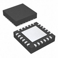


 工商网监
湘ICP备2023018690号
工商网监
湘ICP备2023018690号
