TPS40304A
www.ti.com
SLUSA30 – FEBRUARY 2010
3-V TO 20-V INPUT SYNCHRONOUS BUCK CONTROLLER
Check for Samples: TPS40304A
CONTENTS
FEATURES
1
•
•
•
•
•
•
•
•
•
•
•
Input Voltage Range from 3 V to 20 V
Fixed 600-kHz Switching Frequency
High- and Low-Side FET RDS(on) Current
Sensing
Programmable Thermally Compensated OCP
Levels
Programmable Soft-Start
591-mV, 1% Reference Voltage
Voltage Feed-Forward Compensation
Supports Pre-Biased Output
Frequency Spread Spectrum
Thermal Shutdown Protection at 145°C
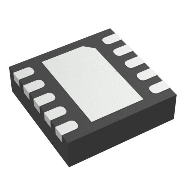
10-Pin 3 mm × 3 mm SON Package with
Ground Connection to Thermal Pad
Device Ratings
2
Electrical Characteristics
3
Device Information
8
Application Information
10
Additional References
13
X
APPLICATIONS
•
•
•
•
POL Modules
Printer
Digital TV
Telecom
DESCRIPTION
The TPS40304A is a cost-optimized synchronous buck controller that operates from 3-V to 20-V input. The
controller implements a voltage-mode control architecture with input-voltage feed-forward compensation that
responds instantly to input voltage change. The switching frequency is fixed at 600 kHz.
Frequency Spread Spectrum feature adds dither to the switching frequency, significantly reducing the peak EMI
noise and making it much easier to comply with EMI standards.
The TPS40304A offers design with a variety of user programmable functions, including soft-start, overcurrent
protection (OCP) levels, and loop compensation.
The OCP level is programmed by a single external resistor connected from LDRV pin to circuit ground. During
initial power on, the TPS40304A enters a calibration cycle, measures the voltage at the LDRV pin, and sets an
internal OCP voltage level. During operation, the programmed OCP voltage level is compared to the voltage drop
across the low-side FET when it is on to determine whether there is an overcurrent condition. The TPS40304A
then enters a shutdown and restart cycle until the fault is removed.
SIMPLIFIED APPLICATION DIAGRAM
VOUT
VIN
TPS40304A
5
FB
BOOT
6
4
COMP
HDRV
7
3
PGOOD
SW
8
2
EN/SS LDRV/OC
9
1
VDD
VOUT
SD
VIN
BP 10
GND
PAD
UDG-10008
1
Please be aware that an important notice concerning availability, standard warranty, and use in critical applications of Texas
Instruments semiconductor products and disclaimers thereto appears at the end of this data sheet.
PRODUCTION DATA information is current as of publication date.
Products conform to specifications per the terms of the Texas
Instruments standard warranty. Production processing does not
necessarily include testing of all parameters.
Copyright © 2010, Texas Instruments Incorporated
�TPS40304A
SLUSA30 – FEBRUARY 2010
www.ti.com
This integrated circuit can be damaged by ESD. Texas Instruments recommends that all integrated circuits be handled with
appropriate precautions. Failure to observe proper handling and installation procedures can cause damage.
ESD damage can range from subtle performance degradation to complete device failure. Precision integrated circuits may be more
susceptible to damage because very small parametric changes could cause the device not to meet its published specifications.
ORDERING INFORMATION
OPERATING FREQUENCY
600 kHz
PACKAGE
TAPE AND REEL QUANTITY
PART NUMBER
250
TPS40304ADRCT
3000
TPS40304ADRCR
Plastic 10-Pin SON (DRC)
ABSOLUTE MAXIMUM RATINGS
over operating free-air temperature range (unless otherwise noted) (1)
VALUE
UNIT
VDD
–0.3 to 22
V
SW
–3 to 27
V
–5
V
BOOT
–0.3 to 30
V
HDRV
–5 to 30
V
BOOT-SW, HDRV-SW (differential from BOOT or HDRV to SW)
–0.3 to 7
V
COMP, PGOOD, FB, BP, LDRV, EN/SS
–0.3 to 7
V
SW (< 100 ns pulse width, 10 µJ)
TJ
Operating junction temperature range
–40 to 145
°C
Tstg
Storage temperature
–55 to 150
°C
(1)
Stresses beyond those listed under absolute maximum ratings may cause permanent damage to the device. These are stress ratings
only and functional operation of the device at these or any other condition beyond those included under recommended operating
conditions is not implied. Exposure to absolute-maximum-rated conditions for extended periods of time may affect device reliability.
DISSIPATION RATINGS
AIRFLOW (LFM)
RqJA HIGH-K BOARD (1)
(°C/W)
POWER RATING (W)
TA = 25°C
POWER RATING (W)
TA = 85°C
0 (Natural Convection)
47.9
2.08
0.835
200
40.5
2.46
0.987
400
38.2
2.61
1.04
PACKAGE
10-Pin SON (DRC)
(1)
Ratings based on JEDEC High Thermal Conductivity (High K) Board. For more information on the test method, see TI technical brief
(SZZA017).
RECOMMENDED OPERATING CONDITIONS
MIN
VDD
Input voltage
TJ
Operating junction temperature
NOM
MAX
UNIT
3
20
V
–40
125
°C
MAX
UNIT
ELECTROSTATIC DISCHARGE (ESD) PROTECTION
MIN
TYP
Human body model (HBM)
2000
V
Charge device model (CDM)
1500
V
2
Submit Documentation Feedback
Copyright © 2010, Texas Instruments Incorporated
Product Folder Link(s) :TPS40304A
�TPS40304A
www.ti.com
SLUSA30 – FEBRUARY 2010
ELECTRICAL CHARACTERISTICS
TJ = –40°C to 125°C, VVDD = 12 V, all parameters at zero power dissipation (unless otherwise noted)
PARAMETER
TEST CONDITIONS
MIN
TYP
MAX
TJ = 25°C, 3 V < VVDD < 20 V
588
591
594
–40°C < TJ < 125°C,
3 V < VVDD < 20 V
585
591
597
UNIT
VOLTAGE REFERENCE
VFB
FB input voltage
mV
INPUT SUPPLY
VVDD
Input supply voltage range
3
20
V
IDDSD
Shutdown supply current
VEN/SS < 0.2 V
70
100
µA
IDDQ
Quiescent, non-switching
Let EN/SS float, VFB = 1 V
2.5
3.5
mA
V
ENABLE/SOFT-START
VIH
High-level input voltage, EN/SS
0.55
0.70
1.00
VIL
Low-level input voltage, EN/SS
0.27
0.30
0.33
V
ISS
Soft-start source current
8
10
12
µA
VSS
Soft-start voltage level
0.4
0.8
1.3
V
6.2
6.5
6.8
V
70
110
mV
kHz
BP REGULATOR
VBP
Output voltage
IBP = 10 mA
VDO
Regulator dropout voltage, VVDD – VBP
IBP = 25 mA, VVDD = 3 V
fSW
PWM frequency
3 V < VVDD < 20 V
VRAMP (1)
Ramp amplitude
fSWFSS
Frequency spread spectrum frequency
deviation
fMOD
Modulation frequency
OSCILLATOR
540
600
660
VVDD/6.6
VVDD/6
VVDD/5.4
12%
V
fSW
25
KHz
PWM
DMAX
(1)
tON(min)
(1)
tDEAD
Maximum duty cycle
VFB = 0 V, 3 V < VVDD < 20 V
90%
Minimum controllable pulse width
45
75
HDRV off to LDRV on
5
25
35
LDRV off to HDRV on
5
25
30
Gain bandwidth product
10
24
Open loop gain
60
Output driver dead time
ns
ns
ERROR AMPLIFIER
GBWP
AOL
(1)
(1)
IIB
Input bias current (current out of FB pin)
VFB = 0.6 V
IEAOP
Output source current
VFB = 0 V
2
IEAOM
Output sink current
VFB = 1 V
2
(1)
MHz
dB
75
nA
mA
Ensured by design. Not production tested.
Submit Documentation Feedback
Copyright © 2010, Texas Instruments Incorporated
Product Folder Link(s) :TPS40304A
3
�TPS40304A
SLUSA30 – FEBRUARY 2010
www.ti.com
ELECTRICAL CHARACTERISTICS (continued)
TJ = –40°C to 125°C, VVDD = 12 V, all parameters at zero power dissipation (unless otherwise noted)
PARAMETER
TEST CONDITIONS
MIN
TYP
MAX
UNIT
PGOOD
VOV
Feedback upper voltage limit for
PGOOD
646
666
691
VUV
Feedback lower voltage limit for
PGOOD
491
516
541
VPGD-HYST
PGOOD hysteresis voltage at FB
25
40
RPGD
PGOOD pull down resistance
VFB = 0 V, IFB = 5 mA
30
70
Ω
IPGDLK
PGOOD leakage current
541 mV < VFB < 646 mV,
VPGOOD = 5 V
10
20
µA
mV
OUTPUT DRIVERS
RHDHI
High-side driver pull-up resistance
VBOOT – VSW = 5 V, IHDRV = –100 mA
0.8
1.5
2.5
Ω
RHDLO
High-side driver pull-down resistance
VBOOT – VSW = 5 V, IHDRV = 100 mA
0.5
1.0
2.2
Ω
RLDHI
Low-side driver pull-up resistance
ILDRV = -100 mA
0.8
1.5
2.5
Ω
RLDLO
Low-side driver pull-down resistance
ILDRV = 100 mA
0.35
0.60
1.20
Ω
tHRISE
(2)
High-side driver rise time
CLOAD = 5 nF
15
ns
tHFALL
(2)
High-side driver fall time
12
ns
tLRISE
(2)
Low-side driver rise time
15
ns
tLFALL
(2)
Low-side driver fall time
10
ns
Minimum pulse time during short circuit
250
ns
Switch leading-edge blanking pulse time
150
ns
OVERCURRENT PROTECTION
tPSSC(min) (2)
tBLNKH
(2)
VOCH
OC threshold for high-side FET
TJ = 25°C
360
450
580
IOCSET
OCSET current source
TJ = 25°C
9.5
10.0
10.5
mV
µA
VLD-CLAMP
Maximum clamp voltage at LDRV
260
340
400
mV
VOCLOS
OC comparator offset voltage for
low-side FET
TJ = 25°C
–8
8
mV
VOCLPRO (2)
Programmable OC range for low-side
FET
TJ = 25°C
12
300
mV
VTHTC (2)
OC threshold temperature coefficient
(both high-side and low-side)
tOFF
OC retry cycles on EN/SS pin
3000
ppm
4
Cycle
BOOT DIODE
VDFWD
Bootstrap diode forward voltage
IBOOT = 5 mA
0.8
V
145
°C
20
°C
THERMAL SHUTDOWN
TJSD (2)
TJSDH
(2)
4
Junction shutdown temperature
(2)
Hysteresis
Ensured by design. Not production tested.
Submit Documentation Feedback
Copyright © 2010, Texas Instruments Incorporated
Product Folder Link(s) :TPS40304A
�TPS40304A
www.ti.com
SLUSA30 – FEBRUARY 2010
TYPICAL CHARACTERISTICS
SWITCHING FREQUENCY
vs
JUNCTION TEMPERATURE
QUIESCENT CURRENT
vs
JUNCTION TEMPERATURE
2.24
625
620
VVDD = 20 V
IDDQ – Quiescent Current – mA
fSW – Switching Frequency – kHz
2.22
615
610
605
VVDD = 12 V
600
VVDD = 3V
595
590
2.20
2.18
2.16
2.14
585
580
–40 –25 –10
5
20
35
50
65
80
2.12
–40 –25 –10
95 110 125
5
20
35
50
65
Figure 1.
Figure 2.
SHUTDOWN CURRENT
vs
JUNCTION TEMPERATURE
OCSET CURRENT SOURCE
vs
JUNCTION TEMPERATURE
14
70
13
IOCSET – OCSET Current Source– mA
72
68
66
64
62
60
80
95 110 125
TJ – Junction Temperature – °C
TJ – Junction Temperature – °C
IDD(SD)– Shutdown Current – mA
VVDD = 12 V
12
11
10
9
8
7
58
–40 –25 –10
VVDD = 12 V
5
20
35
50
65
80
95 110 125
6
–40 –25 –10
TJ – Junction Temperature – °C
Figure 3.
5
20
35
50
65
80
95 110 125
TJ – Junction Temperature – °C
Figure 4.
Submit Documentation Feedback
Copyright © 2010, Texas Instruments Incorporated
Product Folder Link(s) :TPS40304A
5
�TPS40304A
SLUSA30 – FEBRUARY 2010
www.ti.com
TYPICAL CHARACTERISTICS (continued)
FEEDBACK REFERENCE VOLTAGE
vs
JUNCTION TEMPERATURE
ENABLE HIGH-LEVEL THRESHOLD VOLTAGE
vs
JUNCTION TEMPERATURE
740
VIH – Enable High-Level Threshold Voltage – mV
592.0
VFB – Feedback Reference Voltage – mV
591.5
591.0
590.5
590.0
589.5
589.0
588.5
588.0
–40 –25 –10
5
20
35
50
65
80
720
700
680
660
640
620
–40 –25 –10
95 110 125
TJ – Junction Temperature – °C
20
35
50
65
80
95 110 125
TJ – Junction Temperature – °C
Figure 5.
Figure 6.
ENABLE LOW-LEVEL THRESHOLD VOLTAGE
vs
JUNCTION TEMPERATURE
HIGH-SIDE OVERCURRENT THRESHOLD
vs
JUNCTION TEMPERATURE
303.0
VIL – Enable Low-Level Threshold Voltage – mV
VOCH – High-Side Overcurrent Threshold – mV
600
302.5
302.0
301.5
301.0
300.5
300.0
–40 –25 –10
5
20
35
50
65
80
95 110 125
550
500
450
400
350
–40 –25 –10
TJ – Junction Temperature – °C
Figure 7.
6
5
5
20
35
50
65
80
95 110 125
TJ – Junction Temperature – °C
Figure 8.
Submit Documentation Feedback
Copyright © 2010, Texas Instruments Incorporated
Product Folder Link(s) :TPS40304A
�TPS40304A
www.ti.com
SLUSA30 – FEBRUARY 2010
TYPICAL CHARACTERISTICS (continued)
POWER GOOD THRESHOLD VOLTAGE
vs
JUNCTION TEMPERATURE
SOFT-START VOLTAGE
vs
JUNCTION TEMPERATURE
1000
975
750
Overvoltage
VSS – Soft-Start Voltage – mV
VOV/VUV – Power Good Threshold Voltage – mV
800
700
650
600
550
500
950
925
900
875
850
825
800
450
Undervoltage
400
–40 –25 –10
5
20
35
50
65
775
80
95 110 125
750
–40 –25 –10
TJ – Junction Temperature – °C
Figure 9.
5
20
35
50
65
80
95 110 125
TJ – Junction Temperature – °C
Figure 10.
Submit Documentation Feedback
Copyright © 2010, Texas Instruments Incorporated
Product Folder Link(s) :TPS40304A
7
�TPS40304A
SLUSA30 – FEBRUARY 2010
www.ti.com
DEVICE INFORMATION
TERMINAL CONFIGURATION
The package is an 10-Pin SON (DRC) package. Note: The thermal pad is an electrical ground connection.
FB COMP PGOOD EN/SS VDD
5
4
3
2
1
8
9
10
SW
LDRV/
OC
BP
Thermal Pad
6
7
BOOT HDRV
PIN FUNCTIONS
TERMINAL
I/O
DESCRIPTION
NAME
NO.
BOOT
6
I
Gate drive voltage for the high-side N-channel MOSFET. A 100 nF capacitor (typical) must be connected
between this pin and SW. For low input voltage operation, an external schottky diode from BP to BOOT is
recommended to maximize the gate drive voltage for the high-side.
BP
10
O
Output bypass for the internal regulator. Connect a low ESR bypass ceramic capacitor of 1 µF or greater from
this pin to GND.
COMP
4
O
Output of the error amplifier and connection node for loop feedback components.
EN/SS
2
I
Logic level input which starts or stops the controller via an external user command. Letting this pin float turns
the controller on. Pulling this pin low disables the controller. This is also the soft-start programming pin. A
capacitor connected from this pin to GND programs the soft-start time. The capacitor is charged with an
internal current source of 10 µA. The resulting voltage ramp of this pin is also used as a second non-inverting
input to the error amplifier after a 0.8 V (typical) level shift downwards. Output regulation is controlled by the
internal level shifted voltage ramp until that voltage reaches the internal reference voltage of 591 mV – the
voltage ramp of this pin reaches 1.4 V (typical). Optionally, a 267 kΩ resistor from this pin to BP enables
frequency spread spectrum feature.
FB
5
I
Inverting input to the error amplifier. In normal operation, the voltage on this pin is equal to the internal
reference voltage.
PGOOD
3
O
Open drain power good output.
HDRV
7
O
Bootstrapped gate drive output for the high-side N-channel MOSFET.
LDRV/OC
9
O
Gate drive output for the low-side synchronous rectifier N-channel MOSFET. A resistor from this pin to GND
is also used to determine the voltage level for OCP. An internal current source of 10 µA flows through the
resistor during initial calibration and that sets up the voltage trip point used for OCP.
VDD
1
I
Power input to the controller. Bypass VDD to GND with a low ESR ceramic capacitor of at least 1.0-µF close
to the device.
SW
8
O
Sense line for the adaptive anti-cross conduction circuitry. Serves as common connection for the flying
high-side FET driver.
GND
8
Thermal
Pad
Ground connection to the controller. This is also the thermal pad used to conduct heat from the device. This
connection serves a twofold purpose. The first is to provide an electrical ground connection for the device.
The second is to provide a low thermal impedance path from the device die to the PCB. This pad should be
tied externally to a ground plane.
Submit Documentation Feedback
Copyright © 2010, Texas Instruments Incorporated
Product Folder Link(s) :TPS40304A
�TPS40304A
www.ti.com
SLUSA30 – FEBRUARY 2010
TPS40304A BLOCK DIAGRAM
+
10 mA
Soft Start
0.591 VREF + 12.5%
SS
SS
EN/SS
FB
BP
+
2
SD
VDD
6-V
Regulator
1
+
References
6
BOOT
7
HDRV
8
SW
9
LDRV/OC
OC
0.591 VREF
SD
BP
10
COMP
4
FB
0.591 VREF – 12.5%
Fault
Controller
Clock
BP
Calibration
Circuit
Spread
Spectrum
Oscillator
Clock
PWM
Logic
5
BP
Anti-Cross
Conduction
and
Pre-Bias
Circuit
PWM
+
+
10 mA
0.591 VREF
SS
PGOOD
Thermal
Shutdown
750 kW
3
OC
Threshold
Setting
Fault Controller
OC
PAD
UDG-01009
GND
Submit Documentation Feedback
Copyright © 2010, Texas Instruments Incorporated
Product Folder Link(s) :TPS40304A
9
�TPS40304A
SLUSA30 – FEBRUARY 2010
www.ti.com
APPLICATION INFORMATION
Introduction
The TPS40304A is a cost-optimized synchronous buck controller providing high-end features to construct
high-performance DC/DC converters. Pre-bias capability eliminates concerns about damaging sensitive loads
during startup. Programmable overcurrent protection levels and hiccup overcurrent fault recovery maximize
design flexibility and minimize power dissipation in the event of a prolonged output short. Frequency Spread
Spectrum (FSS) feature reduces peak EMI noise by spreading the initial energy of each harmonic along a
frequency band, thus giving a wider spectrum with lower amplitudes.
Voltage Reference
The 591-mV band gap cell is internally connected to the non-inverting input of the error amplifier. The reference
voltage is trimmed with the error amplifier in a unity gain configuration to remove amplifier offset from the final
regulation voltage. The 1% tolerance on the reference voltage allows the user to design a very accurate power
supply.
Enable Functionality, Startup Sequence and Timing
After input power is applied, an internal current source of 40 µA starts to charge up the soft-start capacitor
connected from EN/SS to GND. When the voltage across that capacitor increases to 0.7 V, it enables the internal
BP regulator followed by a calibration. The total calibration time is about 1.9 ms. See Figure 11. During the
calibration, the device performs in the following way. It disables the LDRV drive and injects an internal 10 µA
current source to the resistor connected from LDRV to GND. The voltage developed across that resistor is then
sampled and latched internally as the OCP trip level until one cycles the input or toggles the EN/SS.
2.0
VIN – Input Voltage – V
VEN/SS
1.6
Calibration
Time
1.9 ms
1.3 V
1.2
0.8
0.7 V
0.4
VSS_INT
0
t – Time – ms
UDG-09159
Figure 11. Startup Sequence and Timing
The voltage at EN/SS is internally clamped to 1.3 V before and/or during calibration to minimize the discharging
time once calibration is complete. The discharging current is from an internal current source of 140 µA and it
pulls the voltage down to 0.4 V. It then initiates the soft-start by charging up the capacitor using an internal
current source of 10 µA. The resulting voltage ramp on this pin is used as a second non-inverting input to the
error amplifier after an 800 mV (typical) downward level-shift; therefore, actual soft-start will not take place until
the voltage at this pin reaches 800 mV.
If EN/SS is left floating, the controller starts automatically. EN/SS must be pulled down to less than 270 mV to
guarantee that the chip is in shutdown mode.
10
Submit Documentation Feedback
Copyright © 2010, Texas Instruments Incorporated
Product Folder Link(s) :TPS40304A
�TPS40304A
www.ti.com
SLUSA30 – FEBRUARY 2010
Soft-Start Time
The soft-start time of the TPS40304A is user programmable by selecting a single capacitor. The EN/SS pin
sources 10 µA to charge this capacitor. The actual output ramp-up time is the amount of time that it takes for the
10 µA to charge the capacitor through a 591-mV range. There is some initial lag due to calibration and an offset
(800 mV) from the actual EN/SS pin voltage to the voltage applied to the error amplifier.
The soft-start is done in a closed loop fashion, meaning that the error amplifier controls the output voltage at all
times during the soft start period and the feedback loop is never open as occurs in duty cycle limit soft-start
schemes. The error amplifier has two non-inverting inputs, one connected to the 591-mV reference voltage, and
the other connected to the offset EN/SS pin voltage. The lower of these two voltages is what the error amplifier
controls the FB pin to. As the voltage on the EN/SS pin ramps up past approximately 1.4 V (800 mV offset
voltage plus the 591-mV reference voltage), the 591-mV reference voltage becomes the dominant input and the
converter has reached its final regulation voltage.
The capacitor required for a given soft-start ramp time for the output voltage is given by Equation 1.
æI
ö
CSS = ç SS ÷ ´ t SS
V
è FB ø
where
•
•
•
•
CSS is the required capacitance on the EN/SS pin (F)
ISS is the soft-start source current (10 µA)
VFB is the feedback reference voltage (591 mV)
tSS is the desired soft-start ramp time (s)
(1)
Oscillator and Frequency Spread Spectrum (FSS)
The oscillator frequency is internally fixed at 600 kHz.
Connecting a resistor with a value of 267 kΩ ± 10% from BP to EN/SS enables the FSS feature. When enabled,
it spreads the internal oscillator frequency over a minimum 12% window using a 25-kHz modulation frequency
with triangular profile. By modulating the switching frequency, side-bands are created. The emission power of the
fundamental switching frequency and its harmonics is distributed into smaller pieces scattered around many
side-band frequencies. The effect significantly reduces the peak EMI noise and makes it much easier for the
resultant emission spectrum to pass EMI regulations.
Overcurrent Protection
Programmable OCP level at LDRV is from 6 mV to 150 mV at room temperature with 3000 ppm temperature
coefficient to help compensate for changes in the low-side FET channel resistance as temperature increases.
With a scale factor of 2, the actual trip point across the low-side FET is in the range of 12 mV to 300 mV. The
accuracy of the internal current source is ±5%. Overall offset voltage, including the offset voltage of the internal
comparator and the amplifier for scale factor of 2, is limited to ±8 mV.
Maximum clamp voltage at LDRV is 340 mV to avoid turning on the low-side FET during calibration and in a
pre-biased condition. The maximum clamp voltage is fixed and it does not change with temperature. If the
voltage drop across ROCSET reaches the 340 mV maximum clamp voltage during calibration (No ROCSET resistor
included), it disables OCP. Once disabled, there is no low-side or high-side current sensing.
OCP level at HDRV is fixed at 450 mV with 3000 ppm temperature coefficient to help compensate for changes in
the high-side FET channel resistance as temperature increases. OCP at HDRV provides pulse-by-pulse current
limiting.
Submit Documentation Feedback
Copyright © 2010, Texas Instruments Incorporated
Product Folder Link(s) :TPS40304A
11
�TPS40304A
SLUSA30 – FEBRUARY 2010
www.ti.com
OCP sensing at LDRV is a true inductor valley current detection, using sample and hold. Equation 2 can be used
to calculate ROCSET:
ææ
ö
æI
öö
ç ç IOUT(max ) - ç P-P ÷ ÷ ´ RDS(on ) - VOCLOS ÷
è 2 øø
ç
÷
ROCSET = ç è
÷
2 ´ IOCSET
ç
÷
ç
÷
è
ø
where
•
•
•
•
•
•
IOCSET is the internal current source
VOCLOS is the overall offset voltage
IP-P is the peak-to-peak inductor current
RDS(on) is the drain to source on-resistance of the low-side FET
IOUT(max) is the trip point for OCP
ROCSET is the resistor used for setting the OCP level
(2)
To avoid overcurrent tripping in normal operating load range, calculate ROCSET using the equation above with:
• The maximum RDS(ON) at room temperature
• The lower limit of VOCLOS (–8 mV) and the lower limit of IOCSET (9.5 µA) from the Electrical Characteristics
table.
• The peak-to-peak inductor current IP-P at minimum input voltage
Overcurrent is sensed across both the low-side FET and the high-side FET. If the voltage drop across either FET
exceeds the OC threshold, a count increments one count. If no OC is detected on either FET, the fault counter
decrements by one count. If three OC pulses are summed, a fault condition is declared which cycles the
soft-start function in a hiccup mode. Hiccup mode consists of four dummy soft-start timeouts followed by a real
one if overcurrent condition is encountered during normal operation, or five dummy soft-start timeouts followed
by a real one if overcurrent condition occurs from the beginning during start. This cycle continues indefinitely until
the fault condition is removed.
Drivers
The drivers for the external high-side and low-side MOSFETs are capable of driving a gate-to-source voltage of
VBP. The LDRV driver for the low-side MOSFET switches between BP and GND, while HDRV driver for the
high-side MOSFET is referenced to SW and switches between BOOT and SW. The drivers have
non-overlapping timing that is governed by an adaptive delay circuit to minimize body diode conduction in the
synchronous rectifier.
Pre-Bias Startup
The TPS40304A contains a circuit to prevent current from being pulled from the output during startup in the
condition the output is pre-biased. There are no PWM pulses until the internal soft-start voltage rises above the
error amplifier input (FB pin), if the output is pre-biased. Once the soft-start voltage exceeds the error amplifier
input, the controller slowly initiates synchronous rectification by starting the synchronous rectifier with a narrow
on time. It then increments that on time on a cycle-by-cycle basis until it coincides with the time dictated by (1-D),
where D is the duty cycle of the converter. This approach prevents the sinking of current from a pre-biased
output, and ensures the output voltage startup and ramp to regulation is smooth and controlled.
12
Submit Documentation Feedback
Copyright © 2010, Texas Instruments Incorporated
Product Folder Link(s) :TPS40304A
�TPS40304A
www.ti.com
SLUSA30 – FEBRUARY 2010
Power Good
The TPS40304A provides an indication that output is good for the converter. This is an open drain signal and
pulls low when any condition exists that would indicate that the output of the supply might be out of regulation.
These conditions include the following:
• VFB is more than ±12.5% from nominal
• Soft-start is active
• A short circuit condition has been detected
NOTE
When there is no power to the device, PGOOD is not able to pull close to GND if an
auxiliary supply is used for the power good indication. In this case, a built in resistor
connected from drain to gate on the PGOOD pull down device makes the PGOOD pin
look approximately like a diode to GND.
Thermal Shutdown
If the junction temperature of the device reaches the thermal shutdown limit of 145°C, the PWM and the oscillator
are turned off and HDRV and LDRV are driven low. When the junction cools to the required level (125°C typical),
the PWM initiates soft start as during a normal power-up cycle.
ADDITIONAL REFERENCES
Related Devices
The devices listed in have characteristics similar to the TPS40304A and may be of interest.
Table 1. Related Devices
DEVICE
TPS40303/4/5
DESCRIPTION
3-V to 20-V Input Synchronous Buck Controller
References
These references, design tools and links to additional references, including design software, may be found at
http://power.ti.com
1. Additional PowerPAD™ information may be found in Applications Briefs (SLMA002A) and (SLMA004).
2. Under The Hood Of Low Voltage DC/DC Converters – SEM1500 Topic 5 – 2002 Seminar Series
3. Understanding Buck Power Stages in Switchmode Power Supplies, (SLVA057), March 1999
4. Designing Stable Control Loops – SEM 1400 – 2001 Seminar Series
Package Outline and Recommended PCB Footprint
The following pages outline the mechanical dimensions of the 10-pin DRC package and provide
recommendations for PCB layout.
Submit Documentation Feedback
Copyright © 2010, Texas Instruments Incorporated
Product Folder Link(s) :TPS40304A
13
�PACKAGE OPTION ADDENDUM
www.ti.com
10-Dec-2020
PACKAGING INFORMATION
Orderable Device
Status
(1)
Package Type Package Pins Package
Drawing
Qty
Eco Plan
(2)
Lead finish/
Ball material
MSL Peak Temp
Op Temp (°C)
Device Marking
(3)
(4/5)
(6)
TPS40304ADRCR
ACTIVE
VSON
DRC
10
3000
RoHS & Green
NIPDAUAG
Level-2-260C-1 YEAR
-40 to 145
304A
TPS40304ADRCT
ACTIVE
VSON
DRC
10
250
RoHS & Green
NIPDAUAG
Level-2-260C-1 YEAR
-40 to 145
304A
(1)
The marketing status values are defined as follows:
ACTIVE: Product device recommended for new designs.
LIFEBUY: TI has announced that the device will be discontinued, and a lifetime-buy period is in effect.
NRND: Not recommended for new designs. Device is in production to support existing customers, but TI does not recommend using this part in a new design.
PREVIEW: Device has been announced but is not in production. Samples may or may not be available.
OBSOLETE: TI has discontinued the production of the device.
(2)
RoHS: TI defines "RoHS" to mean semiconductor products that are compliant with the current EU RoHS requirements for all 10 RoHS substances, including the requirement that RoHS substance
do not exceed 0.1% by weight in homogeneous materials. Where designed to be soldered at high temperatures, "RoHS" products are suitable for use in specified lead-free processes. TI may
reference these types of products as "Pb-Free".
RoHS Exempt: TI defines "RoHS Exempt" to mean products that contain lead but are compliant with EU RoHS pursuant to a specific EU RoHS exemption.
Green: TI defines "Green" to mean the content of Chlorine (Cl) and Bromine (Br) based flame retardants meet JS709B low halogen requirements of


 工商网监
湘ICP备2023018690号
工商网监
湘ICP备2023018690号
