TPS51461
SLUSAD9B – DECEMBER 2010 – REVISED SEPTEMBER 2011
www.ti.com
3.3-V/5-V Input, 6-A, D-CAP+™ Mode Synchronous Step-Down Integrated FETs Converter
With 2-Bit VID
Check for Samples: TPS51461
FEATURES
DESCRIPTION
•
The TPS51461 is a fully integrated synchronous buck
regulator employing D-CAP+™. It is used for up to
5-V step-down where system size is at its premium,
performance and optimized BOM are must-haves.
1
2
•
•
•
•
•
•
Integrated FETs Converter w/TI Proprietary
D-CAP+™ Mode Architecture
6-A Maximum Output Current
Minimum External Parts Count
Support all MLCC Output Capacitor and
SP/POSCAP
Auto Skip Mode
Selectable 700-kHz and 1-MHz Frequency
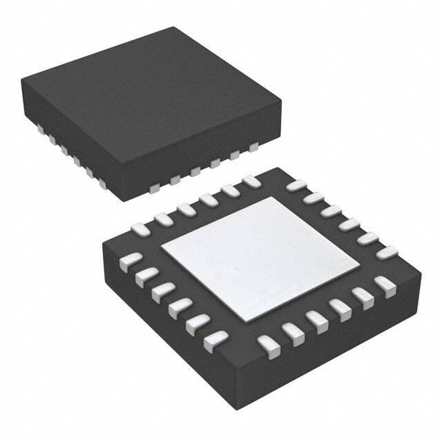
Small 4 × 4, 24-Pin, QFN Package
This device fully supports Intel system
applications with integrated 2-bit VID function.
The TPS51461 also features two switching frequency
settings (700 kHz and 1 MHz), skip mode, pre-bias
startup, programmable external capacitor soft-start
time/voltage transition time, output discharge, internal
VBST Switch, 2-V reference (±1%), power good and
enable.
APPLICATIONS
•
•
agent
The TPS51461 is available in a 4 mm × 4 mm,
24-pin, QFN package (Green RoHs compliant and Pb
free) and is specified from -40°C to 85°C.
Low-Voltage Applications Stepping Down from
5-V or 3.3-V Rail
Notebook/Desktop Computers
+5V
17
16
15
14
13
V5FILT
PGOOD
VID1
VID0
EN
19 PGND
18
V5DRV
ENABLE
VID0
VID1
PGOOD
20 PGND
BST 12
SW 11
21 PGND
SW 10
TPS51461
SW
7
24 VIN
MODE
8
VOUT
SW
SLEW
23 VIN
COMP
9
VREF
SW
GND
VIN
VCCSA
22 VIN
1
2
3
4
5
6
VCCSASNS
UDG-10183
1
2
Please be aware that an important notice concerning availability, standard warranty, and use in critical applications of Texas
Instruments semiconductor products and disclaimers thereto appears at the end of this data sheet.
D-CAP+ is a trademark of Texas Instruments.
PRODUCTION DATA information is current as of publication date.
Products conform to specifications per the terms of the Texas
Instruments standard warranty. Production processing does not
necessarily include testing of all parameters.
Copyright © 2010–2011, Texas Instruments Incorporated
�TPS51461
SLUSAD9B – DECEMBER 2010 – REVISED SEPTEMBER 2011
www.ti.com
These devices have limited built-in ESD protection. The leads should be shorted together or the device placed in conductive foam
during storage or handling to prevent electrostatic damage to the MOS gates.
ORDERING INFORMATION (1)
TA
PACKAGE (2)
ORDERING NUMBER
PINS
OUTPUT SUPPLY
MINIMUM
QUANTITY
-40°C to 85°C
Plastic QFN
(RGE)
TPS51461RGER
24
Tape and reel
3000
TPS51461RGET
24
Mini reel
250
(1)
(2)
ECO PLAN
Green (RoHS and
no Pb/Br)
For the most current package and ordering information, see the Package Option Addendum at the end of this document, or visit the TI
website at www.ti.com.
Package drawings, standard packing quantities, thermal data, symbolization, and PCB design guidelines are available at
www.ti.com/sc/package.
THERMAL INFORMATION
THERMAL METRIC (1)
TPS51461
θJA
Junction-to-ambient thermal resistance
33.6
θJCtop
Junction-to-case (top) thermal resistance
45.0
θJB
Junction-to-board thermal resistance
10.8
ψJT
Junction-to-top characterization parameter
0.2
ψJB
Junction-to-board characterization parameter
10.4
θJCbot
Junction-to-case (bottom) thermal resistance
3.8
(1)
UNITS
RGE (24) PIN
°C/W
For more information about traditional and new thermal metrics, see the IC Package Thermal Metrics application report, SPRA953.
ABSOLUTE MAXIMUM RATINGS (1)
over operating free-air temperature range (unless otherwise noted)
VALUE
Input voltage range
Output voltage range
Electrostatic Discharge
UNIT
MIN
MAX
VIN, EN, MODE
–0.3
7.0
V5DRV, V5FILT, VBST (with respect to SW)
–0.3
7.0
VBST
–0.3
12.5
VID0, VID1
–0.3
3.6
VOUT
–1.0
3.6
SW
–2.0
7.0
SW (transient 20 ns and E=5 µJ)
–3.0
COMP, SLEW, VREF
–0.3
3.6
PGND
–0.3
0.3
PGOOD
–0.3
Human Body Model (HBM)
V
7.0
2000
Charged Device Model (CDM)
V
500
V
Storage temperature
Tstg
–55
150
˚C
Junction temperature
TJ
–40
150
˚C
300
˚C
Lead temperature 1,6 mm (1/16 inch) from case for 10 seconds
(1)
2
Stresses beyond those listed under “absolute maximum ratings” may cause permanent damage to the device. These are stress ratings
only and functional operation of the device at these or any other conditions beyond those indicated under “recommended operating
conditions” is not implied. Exposure to absolute-maximum-rated conditions for extended periods may affect device reliability.
Submit Documentation Feedback
Copyright © 2010–2011, Texas Instruments Incorporated
Product Folder Link(s): TPS51461
�TPS51461
SLUSAD9B – DECEMBER 2010 – REVISED SEPTEMBER 2011
www.ti.com
RECOMMENDED OPERATING CONDITIONS
VALUE
MIN
Input voltage range
Output voltage range
TYP
MAX
VIN, EN, MODE
–0.1
6.5
V5DRV, V5FILT, VBST(with respect to SW)
–0.1
5.5
VBST
–0.1
11.75
VID0, VID1
–0.1
3.5
VOUT
–0.8
2.0
SW
–1.8
6.5
COMP, SLEW, VREF
–0.1
3.5
PGOOD
–0.1
6.5
PGND
–0.1
0.1
-40
85
Ambient temperature range, TA
Submit Documentation Feedback
Copyright © 2010–2011, Texas Instruments Incorporated
Product Folder Link(s): TPS51461
UNIT
V
V
°C
3
�TPS51461
SLUSAD9B – DECEMBER 2010 – REVISED SEPTEMBER 2011
www.ti.com
ELECTRICAL CHARACTERISTICS
over recommended free-air temperature range, VVIN = 5.0 V, VV5DRV = VV5FILT = 5 V, MODE = OPEN, PGND = GND (unless
otherwise noted)
PARAMETER
CONDITIONS
MIN
TYP
MAX
UNIT
SUPPLY: VOLTAGE, CURRENTS AND 5 V UVLO
IVINSD
VIN shutdown current
EN = 'LO'
V5VIN
5VIN supply voltage
V5DRV and V5FILT voltage range
I5VIN
5VIN supply current
EN =’HI’, V5DRV + V5FILT supply current
I5VINSD
5VIN shutdown current
EN = ‘LO’, V5DRV + V5FILT shutdown current
VV5UVLO
V5FILT UVLO
Ramp up; EN = 'HI'
VV5UVHYS
V5FILT UVLO hysteresis
Falling hysteresis
VVREFUVLO
REF UVLO (1)
Rising edge of VREF, EN = 'HI'
VVREFUVHYS
REF UVLO hysteresis (1)
VPOR5VFILT
Reset
4.5
4.2
5
5.0
5.5
1.1
2
mA
10
50
µA
4.3
4.5
440
OVP latch is reset by V5FILT falling below the reset threshold
1.5
µA
0.02
V
V
mV
1.8
V
100
mV
2.3
3.1
0%
1.5%
V
VOLTAGE FEEDBACK LOOP: VREF, VOUT, AND VOLTAGE GM AMPLIFIER
VOUTTOL
VOUT accuracy
VVOUT = 0.8V, No droop
VVREF
VREF
IVREF = 0 µA, TA = 25°C
IVREFSNK
VREF sink current
VREF within tolerance, VVREF = 2.05 V
GM
Transconductance
VDM
Differential mode input voltage
ICOMPSRC
COMP pin maximum sourcing current
VCOMP = 2 V
VOFFSET
Input offset voltage
TA = 25°C
RDSCH
Output voltage discharge resistance
f–3dbVL
–3dB Frequency (1)
–1.5%
2.01
V
2.5
mA
1
mS
0
80
mV
5
mV
–80
–5
0
µA
42
Ω
6
MHz
CURRENT SENSE: CURRENT SENSE AMPLIFIER, OVER CURRENT AND ZERO CROSSING
Gain from the current of the low-side FET to PWM comparator
when PWM = "OFF"
ACSINT
Internal current sense gain
43
IOCL
Positive overcurrent limit (valley)
IOCL(neg)
Negative overcurrent limit (valley)
–6.5
VZXOFF
Zero crossing comp internal offset
0
6
53
57
7.5
mV/A
A
–5.0
A
mV
DRIVERS: BOOT STRAP SWITCH
RDSONBST
Internal BST switch on-resistance
IVBST = 10 mA, TA = 25°C
IBSTLK
Internal BST switch leakage current
VVBST = 14 V, VSW = 7 V, TA = 25°C
(1)
4
5
10
Ω
1
µA
Ensured by design, not production tested.
Submit Documentation Feedback
Copyright © 2010–2011, Texas Instruments Incorporated
Product Folder Link(s): TPS51461
�TPS51461
SLUSAD9B – DECEMBER 2010 – REVISED SEPTEMBER 2011
www.ti.com
ELECTRICAL CHARACTERISTICS (continued)
over recommended free-air temperature range, VVIN = 5.0 V, VV5DRV = VV5FILT = 5 V, MODE = OPEN, PGND = GND (unless
otherwise noted)
PARAMETER
CONDITIONS
MIN
TYP
MAX
Measured at the VOUT pin w/r/t VSLEW
82%
84%
86%
UNIT
PROTECTION: OVP, UVP, PGOOD, and THERMAL SHUTDOWN
VPGDLL
PGOOD deassert to lower
(PGOOD → Low)
VPGHYSHL
PGOOD high hysteresis
VPGDLH
PGOOD de-assert to higher
(PGOOD → Low)
VPGHYSHH
PGOOD high hysteresis
VINMINPG
Minimum VIN voltage for valid
PGOOD
Measured at the VIN pin with a 2-mA sink current on PGOOD
pin
VOVP
OVP threshold
Measured at the VOUT pin w/r/t VSLEW
UVP threshold
Measured at the VOUT pin w/r/t VSLEW, device latches OFF,
begins soft-stop
VUVP
(2)
THSD
Thermal shutdown
THSD(hys)
Thermal Shutdown hysteresis (2)
8%
Measured at the VOUT pin w/r/t VSLEW
114%
116%
118%
-8%
0.9
1.3
1.5
118%
120%
122%
66%
68%
70%
V
130
°C
10
°C
VVIN = 5 V, VVOUT = 0.8 V, fSW = 667 kHz, fixed VID mode
240
ns
VVIN = 5 V, VVOUT = 0.8 V, fSW = 1 MHz, fixed VID mode
160
ns
357
ns
3
ms
Latch off controller, attempt soft-stop.
Controller re-starts after temperature has dropped
TIMERS: ON-TIME, MINIMUM OFF TIME, SS, AND I/O TIMINGS
tONESHOTC
PWM one-shot (2)
tMIN(off)
Minimum OFF time
VVIN = 5 V, VVOUT = 0.8 V, fSW = 1 MHz, DRVL on,
SW = PGND, VVOUT < VSLEW
tPGDDLY
PGOOD startup delay time (excl.
SLEW ramp up time)
Delay starts from VOUT = VID code 00 and excludes SLEW
ramp up time
tPGDPDLYH
PGOOD high propagation delay time
50 mV over drive, rising edge
tPGDPDLYL
PGOOD low propagation delay time
50 mV over drive, falling edge
10
µs
tOVPDLY
OVP delay time
Time from the VOUT pin out of +20% of VSLEW to OVP fault
0.2
µs
tUVDLYEN
Undervoltage fault enable delay (excl. Time from (VOUT = VID code 00) going high to undervoltage
SLEW ramp up time)
fault is ready
3
ms
tUVPDLY
UVP delay time
Time from the VOUT pin out of –30% of VSLEW to UVP fault
ISLEW
Soft-start and voltage transition
CSS = 10 nF assuming voltage slew rate of 1 mV/µs
0.8
1
1.2
µs
8.5
9
10
0
ms
11
µA
LOGIC PINS: I/O VOLTAGE AND CURRENT
VPGDPD
PGOOD pull down voltage
PGOOD low impedance, ISINK = 4 mA, VVIN = VV5FILT = 4.5 V
IPGDLKG
PGOOD leakage current
PGOOD high impedance, forced to 5.5 V
–1
VENH
EN logic high
EN, VCCP logic
0.8
VENL
EN logic low
EN, VCCP logic
IEN
EN input current
VVIDH
VID logic high
VID0, VID1
VVIDL
VID logic low
VID0, VID1
VMODETH
MODE threshold voltage (3)
0.3
V
1
µA
V
0.3
V
1
µA
0.8
V
0.3
MODE 1
0.08
0.13
0.18
MODE 3
0.37
0.42
0.47
MODE 4
0.55
0.60
0.65
MODE 5
0.83
0.88
0.93
MODE 7
1.75
1.80
1.85
V
V
IMODE
MODE current
15
µA
RPD
VID pull-down resistance
10
kΩ
(2)
(3)
Ensured by design, not production tested.
See Table 3 for descriptions of MODE parameters.
Submit Documentation Feedback
Copyright © 2010–2011, Texas Instruments Incorporated
Product Folder Link(s): TPS51461
5
�TPS51461
SLUSAD9B – DECEMBER 2010 – REVISED SEPTEMBER 2011
www.ti.com
VIN
VIN
VIN
PGND
PGND
PGND
RGE PACKAGE
24
23
22
21
20
19
GND
1
18 V5DRV
VREF
2
17 V5FILT
COMP
3
16 PGOOD
TPS51461RGE
6
13 EN
SW
7
8
9
10
11
12
BST
MODE
14 VID0
Thermal Pad
SW
5
SW
VOUT
15 VID1
SW
4
SW
SLEW
PIN FUNCTIONS
PIN
NO.
NAME
I/O
DESCRIPTION
19
20
PGND
I
Power ground. Source terminal of the rectifying low-side power FET. Positive input for current sensing.
VIN
I
Power supply input pin. Drain terminal of the switching high-side power FET.
GND
–
Signal ground.
2
VREF
O
2.0-V reference output. Connect a 0.22-µF ceramic capacitor to GND.
3
COMP
O
Connect series R/C or R between this pin and VREF for loop compensation.
4
SLEW
I/O
Program the startup and voltage transition time using an external capacitor via 10-µA current source.
5
VOUT
I
Output voltage monitor input pin.
6
MODE
I
Allows selection of switching frequencies and output voltage. (See Table 3)
SW
I/O
BST
I
Power supply for internal high-side gate driver. Connect a 0.1-µF bootstrap capacitor between this pin and
the SW pin.
13
EN
I
Enable of the SMPS.
14
VID0
15
VID1
I
2-bit VID input.
16
PGOOD
O
Power good output. Connect pull-up resistor.
17
V5FILT
I
5-V power supply for analog circuits.
18
V5DRV
I
5-V power supply for the gate driver.
21
22
23
24
1
7
8
9
Switching node output. Connect to the external inductor. Also serve as current-sensing negative input.
10
11
12
6
Submit Documentation Feedback
Copyright © 2010–2011, Texas Instruments Incorporated
Product Folder Link(s): TPS51461
�TPS51461
SLUSAD9B – DECEMBER 2010 – REVISED SEPTEMBER 2011
www.ti.com
BLOCK DIAGRAM
14 VID0
10 mA
00
01
10
11
15 VID1
+
VREFIN +8/16 %
+
UV
VREFIN –32%
EN 13
+
+
OV
VREFIN –8/16 %
VREFIN +20%
COMP
16 PGOOD
+
15 mA
3
UVP
Control Logic
On-Time
and LL
Selection
OVP
VS
+
SLEW
4
VREF
2
VOUT
5
6
MODE
12 BST
+
VCS
PWM
22 VIN
23 VIN
Bandgap
24 VIN
8R
+
+
CS
OC
PGND
tON
OneShot
R
7
SW
8
SW
9
SW
XCON
10 SW
11 SW
SW
18 V5DRV
Sense
ZC
+
17 V5FILT
Discharge
GND
1
19
PGND
20
PGND
21
PGND
TPS51461
UDG-10184
Table 1. Intel SA VID
(1)
VID 0
VID 1
0
0
VCCSA
0.9 V
0
1
0.80V (1) MODE = Open
0
1
0.85V (1) MODE = 33 kΩ
1
0
0.725 V
1
1
0.675 V
0.80V for 2011 SV processor and 0.85V for 2011 LV/ULV processor
Submit Documentation Feedback
Copyright © 2010–2011, Texas Instruments Incorporated
Product Folder Link(s): TPS51461
7
�TPS51461
SLUSAD9B – DECEMBER 2010 – REVISED SEPTEMBER 2011
www.ti.com
7
SW
UDG-10185
DNP
10 nF
6
5
8
SW
3
10 kW
TPS51461
4
9
SW
SW 10
0.22 mF
2
1
24 VIN
23 VIN
22 VIN
21 PGND
VIN
10 mF
VID0
VID1
PGOOD
10 mF 0.1 mF
19 PGND
2 kW
ENABLE
20 PGND
17
100 kW
0W
2.2 mF
GND
V5DRV
18
V5FILT
VREF
1 mF
SW 11
PGOOD
+5V
BST 12
2 kW
15
VID1
SLEW
16
13
VID0
VOUT
14
EN
MODE
COMP
2 kW
0.1 mF
DNP
DNP
L
0.42 mH
22 mF
22 mF
22 mF
22 mF 22 mF 22 mF
VCCSA
VCCSASNS
APPLICATION SCHEMATIC WITH TPS51461
Figure 1. Application Schematic Using Droop Configuration,
and Recommended Reference Design for Intel SA Application
8
Submit Documentation Feedback
Copyright © 2010–2011, Texas Instruments Incorporated
Product Folder Link(s): TPS51461
�Copyright © 2010–2011, Texas Instruments Incorporated
Product Folder Link(s): TPS51461
VIN
VID0
VID1
PGOOD
10 mF
10 mF 0.1 mF
0.22 mF
2
1
24 VIN
23 VIN
22 VIN
21 PGND
20 PGND
19 PGND
17
V5FILT
18
V5DRV
GND
5 kW
3.3 nF
3
4
TPS51461
10 nF
5
6
8
7
SW
SW
DNP
9
SW
SW 10
SW 11
BST 12
13
14
15
16
2 kW
0.1 mF
2 kW
DNP
DNP
L
0.42 mH
22 mF
22 mF
22 mF 22 mF
UDG-10186
VCCSASNS
100 W
VCCSA
www.ti.com
VREF
100 kW
PGOOD
ENABLE
COMP
0W
VID1
SLEW
2.2 mF
VID0
VOUT
1 mF
EN
MODE
+5V
TPS51461
SLUSAD9B – DECEMBER 2010 – REVISED SEPTEMBER 2011
Figure 2. Application Schematic Using Non-Droop Configuration
Submit Documentation Feedback
9
�TPS51461
SLUSAD9B – DECEMBER 2010 – REVISED SEPTEMBER 2011
www.ti.com
Application Circuit List of Materials
Recommended parts for key external components for the circuits in Figure 1 and Figure 2 are listed in Table 2.
Table 2. Key External Component Recommendations
(Figure 1 and Figure 2)
FUNCTION
MANUFACTURER
PART NUMBER
Output Inductor
Nec-Tokin
MPCG0740LR42C
Panasonic
ECJ2FB0J226M
Murata
GRM21BR60J226ME39L
Ceramic Output Capacitors
10
Submit Documentation Feedback
Copyright © 2010–2011, Texas Instruments Incorporated
Product Folder Link(s): TPS51461
�TPS51461
SLUSAD9B – DECEMBER 2010 – REVISED SEPTEMBER 2011
www.ti.com
APPLICATION INFORMATION
Functional Overview
The TPS51461 is a D-CAP+™ mode adaptive on-time converter. The output voltage is set using a 2-bit DAC that
outputs a reference voltage in accordance with the code defined in Table 1. VID-on-the-fly transitions are
supported with the slew rate controlled by a single capacitor on the SLEW pin. Integrated high-side and low-side
FET supports output current to a maximum of 6-ADC. The converter automatically runs in discontinuous
conduction mode (DCM) to optimize light-load efficiency. Two switching frequency selections are provided, (700
kHz and 1 MHz) to enable optimization of the power chain for the cost, size and efficiency requirements of the
design.
In adaptive on-time converters, the controller varies the on-time as a function of input and output voltage to
maintain a nearly constant frequency during steady-state conditions. In conventional constant on-time converters,
each cycle begins when the output voltage crosses to a fixed reference level. However, in the TPS51461, the
cycle begins when the current feedback reaches an error voltage level which is the amplified difference between
the reference voltage and the feedback voltage.
PWM Operation
Referring to Figure 3, in steady state, continuous conduction mode, the converter operates in the following way.
Starting with the condition that the top FET is off and the bottom FET is on, the current feedback (VCS) is higher
than the error amplifier output (VCOMP). VCS falls until it hits VCOMP, which contains a component of the output
ripple voltage. VCS is not directly accessible by measuring signals on pins of TPS51461. The PWM comparator
senses where the two waveforms cross and triggers the on-time generator.
Current
Feedback
Voltage (V)
VCS
VCOMP
VREF
tON
t
Time (ms)
UDG-10187
Figure 3. D-CAP+™ Mode Basic Waveforms
The current feedback is an amplified and filtered version of the voltage between PGND and SW during low-side
FET on-time. The TPS51461 also provides a single-ended differential voltage (VOUT) feedback to increase the
system accuracy and reduce the dependence of circuit performance on layout.
Submit Documentation Feedback
Copyright © 2010–2011, Texas Instruments Incorporated
Product Folder Link(s): TPS51461
11
�TPS51461
SLUSAD9B – DECEMBER 2010 – REVISED SEPTEMBER 2011
www.ti.com
PWM Frequency and Adaptive on Time Control
In general, the on-time (at the SW node) can be estimated byEquation 1.
V
1
tON = OUT ´
VIN
fSW
where
•
fSW is the frequency selected by the connection of the MODE pin
(1)
The on-time pulse is sent to the top FET. The inductor current and the current feedback rises to peak value.
Each ON pulse is latched to prevent double pulsing. Switching frequency settings are shown in Table 3.
Non-Droop Configuration
The TPS51461 can be configured as a non-droop solution. The benefit of a non-droop approach is that load
regulation is flat, therefore, in a system where tight DC tolerance is desired, the non-droop approach is
recommended. For the Intel system agent application, non-droop is recommended as the standard configuration.
The non-droop approach can be implemented by connecting a resistor and a capacitor between the COMP and
the VREF pins. The purpose of the type II compensation is to obtain high DC feedback gain while minimizing the
phase delay at unity gain cross over frequency of the converter.
The value of the resistor (RC) can be calculated using the desired unity gain bandwidth of the converter, and the
value of the capacitor (CC) can be calculated by knowing where the zero location is desired. An application tool
that calculates these values is available from your local TI Field Application Engineer.
Figure 4 shows the basic implementation of the non-droop mode using the TPS51461.
GMV = 1 mS
VSLEW
RC
CC
+
+
–
RDS(on)
LOUT
+
GMC= 1 mS
Driver
+
PWM
Comparator
ROUT
RLOAD
COUT
8 kW
+
–
ESR
VREF
UDG-10190
Figure 4. Non-Droop Mode Basic Implementation
Figure 5 shows the load regulation of the system agent rail using non-droop configuration.
Figure 6 shows the transient response of TPS51461 using non-droop configuration where COUT = 4 × 22 µF. The
applied step load is from 0 A to 2 A.
12
Submit Documentation Feedback
Copyright © 2010–2011, Texas Instruments Incorporated
Product Folder Link(s): TPS51461
�TPS51461
SLUSAD9B – DECEMBER 2010 – REVISED SEPTEMBER 2011
www.ti.com
0.87
Output Voltage (V)
0.85
0.83
0.81
0.79
0.77
Mode 3
Mode 4
Mode 7
Mode 8
0.75
0.73
0
1
VIN = 5 V
2
3
4
Output Current (A)
5
Figure 5. 0.8-V Load Regulation (VIN = 5 V)
Non-Droop Configuration
6
Figure 6. Non-Droop Configuration Transient
Response
Droop Configuration
The terminology for droop is the same as load line or voltage positioning as defined in the Intel CPU VCORE
specification. Based on the actual tolerance requirement of the application, load-line set points can be defined to
maximize either cost savings (by reducing output capacitors) or power reduction benefits.
Accurate droop voltage response is provided by the finite gain of the droop amplifier. The equation for droop
voltage is shown in Equation 2.
´ I(L)
A
VDROOP = CSINT
RDROOP ´ GM
where
•
•
•
•
•
low-side on-resistence is used as the current sensing element
ACSINT is a constant, which nominally is 53 mV/A.
I(L) is the DC current of the inductor, or the load current
RDROOP is the value of resistor from the COMP pin to the VREF pin
GM is the transconductance of the droop amplifier with nominal value of 1 mS
V
A CSINT
A CSINT
\ RDROOP =
RLOAD _ LINE = DROOP =
I(L)
RDROOP ´ GM
RLOAD _ LINE ´ GM
(2)
(3)
Therefore, if a 5-mΩ load line to the system agent rail is desired, the calculated RDROOP is approximately 10 kΩ.
Equation 2 can be used to easily derive RDROOP for any load line slope/droop design target.
Submit Documentation Feedback
Copyright © 2010–2011, Texas Instruments Incorporated
Product Folder Link(s): TPS51461
13
�TPS51461
SLUSAD9B – DECEMBER 2010 – REVISED SEPTEMBER 2011
www.ti.com
Figure 7 shows the basic implementation of the droop mode using the TPS51461.
GMV = 1 mS
VSLEW
RDROOP
+
+
–
RDS(on)
LOUT
+
GMC= 1 mS
Driver
+
PWM
Comparator
ROUT
RLOAD
COUT
8 kW
+
–
ESR
VREF
UDG-10188
Figure 7. DROOP Mode Basic Implementation
The droop (voltage positioning) method was originally recommended to reduce the number of external output
capacitors required. The effective transient voltage range is increased because of the active voltage positioning
(see Figure 8).
Lead insertion
ILOAD
Lead release
Droop
VOUT setpoint at 0 A
Maximum transient voltage
= (5%–1%) x 2 = 8% x VOUT
VOUT setpoint at 6 A
NonDroop
Maximum overshoot voltage =(5%–1%) x 1 = 4% x VOUT
VOUT setpoint at 0 A
Maximum undershoot voltage =(5%–1%) x 1 = 4% x VOUT
UDG-10189
Figure 8. DROOP vs Non-DROOP in Transient Voltage Window
14
Submit Documentation Feedback
Copyright © 2010–2011, Texas Instruments Incorporated
Product Folder Link(s): TPS51461
�TPS51461
SLUSAD9B – DECEMBER 2010 – REVISED SEPTEMBER 2011
www.ti.com
Consider an example of 0.8 V ±5%. If no droop is permitted, the allowable transient overshoot can be at a
maximum of +4%; the allowed transient undershoot can only be at minimum of –4% (given a dc tolerance of
±1%). Therefore, the overshoot and undershoot window is only ±32 mV. If the droop method is applied, this
overshoot and undershoot window could be potentially doubled from ±32 mV to ±64 mV, given the same load
step and release.
In applications where the DC and the AC tolerances are not separated, which means there is not a strict DC
tolerance requirement, the droop method can be used.
Table 3. Mode Parameter Table
MODE
CONNECTION
MODE
COMPENSATION
TECHNOLOGY
DROOP
NONDROOP
VREF (V)
SWITCHING
FREQUENCY
(fSW)
VID1 = 1
VID0 = 0
(V)
1
GND
X
2.06
1 MHz
0.80
3
22 kΩ
X
X
2.01
700 kHz
0.80
4
33 kΩ
X
X
2.01
1 MHz
0.85
5
47 kΩ
X
2.06
1 MHz
0.85
7
100 kΩ
X
X
2.01
700 kHz
0.85
8
Open
X
X
2.01
1 MHz
0.80
Figure 9 shows the load regulation of the 0.8-V rail using an RDROOP value of 10 kΩ.
Figure 10 shows the transient response of the TPS51461 using droop configuration and COUT = 4 × 22 µF. The
applied step load is from 0 A to 2 A.
0.84
0.83
Output Voltage (V)
0.82
0.81
0.80
0.79
0.78
0.77
0.76
0.75
VIN = 3.3 V
0
1
2
3
4
Output Current (A)
5
Figure 9. 0.8-V Load Regulation (VIN = 3.3 V)
6
Figure 10. Droop Configuration Transient
Response
Submit Documentation Feedback
Copyright © 2010–2011, Texas Instruments Incorporated
Product Folder Link(s): TPS51461
15
�TPS51461
SLUSAD9B – DECEMBER 2010 – REVISED SEPTEMBER 2011
www.ti.com
Light Load Power Saving Features
The TPS51461 has an automatic pulse-skipping mode to provide excellent efficiency over a wide load range.
The converter senses inductor current and prevents negative flow by shutting off the low-side gate driver. This
saves power by eliminating re-circulation of the inductor current. Further, when the bottom FET shuts off, the
converter enters discontinuous mode, and the switching frequency decreases, thus reducing switching losses as
well.
Voltage Slewing
The TPS51461 ramps the SLEW voltage up and down to perform the output voltage transitioning. The timing is
independent of switching frequency, as well as output resistive and capacitive loading. It is set by a capacitor
from SLEW pin to GND, called CSLEW, together with an internal current source of 10 µA. The slew rate is used to
set the startup and voltage transition rate.
I
CSLEW = SLEW
SR
(4)
CSLEW ´ 0.9 V
tSS =
ISLEW
where
•
•
ISLEW = 10 µA (nom)
SR is the target output voltage slew rate, per Intel specification between 0.5 mV/µs and 10 mV/µs
(5)
For the current reference design, an SR of 1 mV/µs is targeted. The CSLEW is calculated to be 10 nF. The slower
slew rate is desired to minimize large inductor current perturbation during startup and voltage transitioning thus
reducing the possibility of acoustic noise.
After the power up, when VID1 is transitioning from 0 to 1, TPS51461 follows the SLEW voltage entering the
forced PWM mode to actively discharge the output voltage from 0.9 V to 0.8 V. The actual output voltage slew
rate is approximately the same as the set slew rate while the bandwidth of the converter supports it and there is
no overcurrent triggered by additional charging current flowing into the output capacitors. After SLEW transition is
completed, PWM mode is maintained for 64 µs (16 clock cycles when the frequency is 1 MHz) to ensure voltage
regulation.
Protection Features
The TPS51461 offers many features to protect the converter power chain as well as the system electronics.
5-V Undervoltage Protection (UVLO)
The TPS51461 continuously monitors the voltage on the V5FILT pin to ensure that the voltage level is high
enough to bias the device properly and to provide sufficient gate drive potential to maintain high efficiency. The
converter starts with approximately 4.3 V and has a nominal of 440 mV of hysteresis. If the 5-V UVLO limit is
reached, the converter transitions the phase node into a 3-state function. And the converter remains in the off
state until the device is reset by cycling 5 V until the 5-V POR is reached (2.3-V nominal). The power input does
not have an UVLO function
Power Good Signals
The TPS51461 has one open-drain power good (PGOOD) pin. During startup, there is a 3 ms power good delay
starting from the output voltage reaching the regulation point (excluding soft-start ramp-up time). And there is
also a 1 ms power good high propagation delay. The PGOOD pin de-asserts as soon as the EN pin is pulled low
or an undervoltage condition on V5FILT is detected. The PGOOD signal is blanked during VID voltage transitions
to prevent false triggering during voltage slewing.
16
Submit Documentation Feedback
Copyright © 2010–2011, Texas Instruments Incorporated
Product Folder Link(s): TPS51461
�TPS51461
www.ti.com
SLUSAD9B – DECEMBER 2010 – REVISED SEPTEMBER 2011
Output Overvoltage Protection (OVP)
In addition to the power good function described above, the TPS51461 has additional OVP and UVP thresholds
and protection circuits.
An OVP condition is detected when the output voltage is approximately 120% × VSLEW. In this case, the
converter de-asserts the PGOOD signals and performs the overvoltage protection function. The converter
remains in this state until the device is reset by cycling 5 V until the 5-V POR threshold (2.3 V nominal) is
reached.
Output Undervoltage Protection (UVP)
Output undervoltage protection works in conjunction with the current protection described in the Overcurrent
Protection and Overcurrent Limit sections. If the output voltage drops below 70% of VSLEW, after an 8-µs delay,
the device latches OFF. Undervoltage protection can be reset only by EN or a 5-V POR.
Overcurrent Protection
Both positive and negative overcurrent protection are provided in the TPS51461:
• Overcurrent Limit (OCL)
• Negative OCL (level same as positive OCL)
Overcurrent Limit
If the sensed current value is above the OCL setting, the converter delays the next ON pulse until the current
drops below the OCL limit. Current limiting occurs on a pulse-by-pulse basis. The TPS51461 uses a valley
current limiting scheme where the DC OCL trip point is the OCL limit plus half of the inductor ripple current. The
minimum valley OCL is 6 A over process and temperature.
During the overcurrent protection event, the output voltage likely droops until the UVP limit is reached. Then, the
converter de-asserts the PGOOD pin, and then latches OFF after an 8-µs delay. The converter remains in this
state until the device is reset by EN or a 5VFILT POR.
1
IOCL(dc ) = IOCL(valley ) + ´ IP-P
2
(6)
Negative OCL
The negative OCL circuit acts when the converter is sinking current from the output capacitor(s). The converter
continues to act in a valley mode, the absolute value of the negative OCL set point is typically -6.5 A.
Thermal Protection
Thermal Shutdown
The TPS51461 has an internal temperature sensor. When the temperature reaches a nominal 130°C, the device
shuts down until the temperature cools by approximately 10°C. Then the converter restarts.
Submit Documentation Feedback
Copyright © 2010–2011, Texas Instruments Incorporated
Product Folder Link(s): TPS51461
17
�TPS51461
SLUSAD9B – DECEMBER 2010 – REVISED SEPTEMBER 2011
www.ti.com
Startup and VID Transition Timing Diagrams
1.05-V Rail
0.95 V
VCCP
EN
Internal Enable
VID1 (3)
VID0 (3)
SLEW (1 mV/ms)
VOUT
VCCSA_PGOOD
Reset Time (2)
UNCORE_PWRGD (1)
260 ms
900 ms
4 ms
2.5 ms
UDG-10191
Figure 11. Fixed VID/Fixed Step Startup and VID Toggle Timing Diagram for 2011 Intel Platform
For Figure 11:
(1) Includes VCCA, VCCAXG, and VDDQ power rails.
(2) Processor reset: VID transition must be completed by this time.
(3) 1-kΩ pull-down resistor required.
18
Submit Documentation Feedback
Copyright © 2010–2011, Texas Instruments Incorporated
Product Folder Link(s): TPS51461
�TPS51461
SLUSAD9B – DECEMBER 2010 – REVISED SEPTEMBER 2011
www.ti.com
1.05-V Rail
0.95 V
VCCP
EN
100ms
Internal Enable
VID1 (3)
VID0 (3)
SLEW (1 mV/ms)
VOUT
VCCSA_PGOOD
Reset Time (2)
UNCORE_PWRGD (1)
260 ms
900 ms
4 ms
2.5 ms
UDG-10192
Figure 12. Fixed VID/Fixed Step Startup and VID Toggle Timing Diagram for 2012 Intel Platform
For Figure 12:
(1) Includes VCCA, VCCAXG, and VDDQ power rails.
(2) Processor reset: VID transition must be completed by this time.
(3) 1-kΩ pull-down resistor required.
Submit Documentation Feedback
Copyright © 2010–2011, Texas Instruments Incorporated
Product Folder Link(s): TPS51461
19
�TPS51461
SLUSAD9B – DECEMBER 2010 – REVISED SEPTEMBER 2011
www.ti.com
TYPICAL CHARACTERISTICS
90
90
TA = 25°C
VIN = 3.3 V
TA = 25°C
VIN = 5 V
85
80
80
75
75
Efficiency (%)
70
65
60
Mode 1
Mode 3
Mode 4
Mode 7
Mode 8
55
50
45
40
0.01
0.1
1
Output Current (A)
70
65
60
Mode 1
Mode 3
Mode 4
Mode 7
Mode 8
55
50
45
40
0.01
10
0.1
1
Output Current (A)
Figure 13. Efficiency vs Output Current
Figure 14. Efficiency vs Output Current
1.25
1.25
Mode 1
Mode 3
Mode 4
Mode 7
Mode 8
Mode 1
Mode 3
Mode 4
Mode 7
Mode 8
1.00
Power Loss (W)
Power Loss (W)
1.00
0.75
0.50
0.25
0.75
0.50
0.25
TA = 25°C
VIN = 3.3 V
0.00
0.1
1
Output Current (A)
TA = 25°C
VIN = 5 V
0.00
0.1
10
1
Output Current (A)
Figure 15. Power Loss
350
30
310
40
Gain
30
260
250
20
210
150
-20
100
-30
-50
1000
10 k
10
160
0
Phase
-10
50
100 k
1M
0
10 M
110
-20
-30
25°C
-10°C
85°C
-40
Gain (dB)
200
Phase
-10
Phase (°)
10
Gain
300
20
Gain (dB)
360
60
50
40
-40
60
25°C
-10°C
85°C
-50
1000
10 k
Frequency (Hz)
10
100 k
1M
-40
10 M
Frequency (Hz)
Figure 17. Bode Plot (Non-Droop Mode) VIN = 5 V,
VOUT = 0.8 V, ILOAD = 5 A
20
10
Figure 16. Power Loss
400
50
0
10
Phase (°)
Efficiency (%)
85
Figure 18. Bode Plot (Droop Mode), VIN = 5 V,
VOUT = 0.8 V, ILOAD = 5 A
Submit Documentation Feedback
Copyright © 2010–2011, Texas Instruments Incorporated
Product Folder Link(s): TPS51461
�TPS51461
SLUSAD9B – DECEMBER 2010 – REVISED SEPTEMBER 2011
www.ti.com
TYPICAL CHARACTERISTICS (continued)
Figure 19. Mode 8 Non-Droop, 0 A
Figure 20. Mode 8 Non-Droop, 3 A
Figure 21. Mode 8 Droop, 0 A
Figure 22. Mode 8 Droop, 3 A
Figure 23. Mode 4 Non-Droop 0 A
Figure 24. Mode 4 Non-Droop 3 A
Submit Documentation Feedback
Copyright © 2010–2011, Texas Instruments Incorporated
Product Folder Link(s): TPS51461
21
�TPS51461
SLUSAD9B – DECEMBER 2010 – REVISED SEPTEMBER 2011
www.ti.com
TYPICAL CHARACTERISTICS (continued)
Figure 25. Mode 4 Droop 0 A
22
Figure 26. Mode 4 Droop 3 A
Submit Documentation Feedback
Copyright © 2010–2011, Texas Instruments Incorporated
Product Folder Link(s): TPS51461
�TPS51461
SLUSAD9B – DECEMBER 2010 – REVISED SEPTEMBER 2011
www.ti.com
DESIGN PROCEDURE
The simplified design procedure is done for a non-droop application using the TPS51461 converter.
Step One
Determine the specifications.
The System Agent Rail requirements provide the following key parameters:
1. V00 = 0.90 V
2. V10 = 0.80 V
3. ICC(max) = 6 A
4. IDYN(max) = 2 A
5. ICC(tdc) = 3 A
Step Two
Determine system parameters.
The input voltage range and operating frequency are of primary interest. For example:
1. VIN = 5 V
2. fSW = 1 MHz
Step Three
Determine inductor value and choose inductor.
Smaller values of inductor have better transient performance but higher ripple and lower efficiency. Higher values
have the opposite characteristics. It is common practice to limit the ripple current to 25% to 50% of the maximum
current. In this case, use 25%:
IP-P = 6 A ´ 0.25 = 1.5 A
(7)
At fSW = 1 MHz, with a 5-V input and a 0.80-V output:
ö
V10
÷÷
è (fSW ´ VIN ) ø
æ
L=
V ´ dT
=
IP-P
(VIN - V10 )´ çç
IP-P
æ 0.8 ö
÷÷
è (1´ 5 ) ø
(5 - 0.8 )´ çç
=
1.5 A
= 0.45 mH
(8)
For this application, a 0.42-µH, 1.55-mΩ inductor from NEC-TOKIN with part number MPCG0740LR42C is
chosen.
Step Four
Set the output voltage.
The output voltage is determined by the VID settings. The actual voltage set point for each VID setting is listed in
Table 1. No external resistor dividers are needed for this design.
Step Five
Calculate CSLEW.
VID pin transition and soft-start time is determined by CSLEW and 10 µA of internal current source.
I
10 mA
= 10nF
CSLEW = SLEW =
SRDAC 1 mV
ms
(9)
The slower slew rate is desired to minimize large inductor current perturbation during startup and voltage
transition, thus reducing the possibility of acoustic noise.
Submit Documentation Feedback
Copyright © 2010–2011, Texas Instruments Incorporated
Product Folder Link(s): TPS51461
23
�TPS51461
SLUSAD9B – DECEMBER 2010 – REVISED SEPTEMBER 2011
www.ti.com
Given the CSLEW, use Equation 10 to calculate the soft start time.
´ 0.9 V 10nF ´ 0.9 V
C
=
= 900 ms
tSS = SLEW
ISLEW
10 mA
(10)
Step Six
Calculate OCL.
The DC OCL level of TPS51461 design is determined by Equation 11,
1
1
IOCL(dc ) = IOCL(valley ) + ´ IP-P = 6 A + ´ 1.5 A = 6.75 A
2
2
(11)
The minimum valley OCL is 6 A over process and temperature, and IP-P = 1.5 A, the minimum DC OCL is
calculated to be 6.75A.
Step Seven
Determine the output capacitance.
To determine COUT based on transient and stability requirement, first calculate the the minimum output
capacitance for a given transient.
Equation 13 and Equation 12 can be used to estimate the amount of capacitance needed for a given dynamic
load step/release. Please note that there are other factors that may impact the amount of output capacitance for
a specific design, such as ripple and stability. Equation 13 and Equation 12 are used only to estimate the
transient requirement, the result should be used in conjunction with other factors of the design to determine the
necessary output capacitance for the application.
æV
ö
´t
L ´ DILOAD(max )2 ´ ç VOUT SW + tMIN(off ) ÷
ç VIN(min )
÷
è
ø
COUT(min_ under ) =
ææ V
ö
ö
IN(min ) - VVOUT
÷
÷ ´ tSW - t
2 ´ DVLOAD(insert ) ´ ç ç
MIN(off ) ÷ ´ VVOUT
çç
÷
VIN(min )
ø
èè
ø
COUT(min_ over ) =
(
(12)
2
LOUT ´ DILOAD(max )
)
2 ´ DVLOAD(release ) ´ VVOUT
(13)
Equation 12 and Equation 13 calculate the minimum COUT for meeting the transient requirement, which is
72.9 µF assuming the following:
• ±3% voltage allowance for load step and release
• MLCC capacitance derating of 60% due to DC and AC bias effect
In this reference design, 4, 22-µF capacitors are used in order to provide this amount of capacitance.
24
Submit Documentation Feedback
Copyright © 2010–2011, Texas Instruments Incorporated
Product Folder Link(s): TPS51461
�TPS51461
SLUSAD9B – DECEMBER 2010 – REVISED SEPTEMBER 2011
www.ti.com
Step Eight
Determine the stability based on the output capacitance COUT.
In order to achieve stable operation. The 0-dB frequency, f0 should be kept less than 1/5 of the switching
frequency (1 MHz). (See Figure 4)
R
GM
1
´
´ C = 150kHz
f0 =
2p COUT RS
where
•
RS = RDS(on) × GMC × RLOAD
(14)
.
f ´ RS ´ 2p ´ COUT 150kHz ´ 53mW ´ 2p ´ 88 mF
=
» 5kW
RC = 0
GM
1mS
(15)
Using 4, 22-µF capacitors, the compensation resistance, RC can be calculated to be approximately 5 kΩ.
The purpose of the comparator capacitor (CC) is to reduce the DC component to obtain high DC feedback gain.
However, as it causes phase delay, another zero to cancel this effect at f0 is needed. This zero can be
determined by values of CC and the compensation resistor, RC.
f
1
= 0
fZ =
2p ´ RC ´ CC 10
(16)
And since RC has previously been derived, the value of CC is calculated to be 2.2 nF. In order to further boost
phase margin, a value of 3.3-nF is chosen for this reference design.
Step Nine
Select decoupling and peripheral components.
For TPS51461 peripheral capacitors use the following minimum values of ceramic capacitance. X5R or better
temperature coefficient is recommended. Tighter tolerances and higher voltage ratings are always appropriate.
• V5DRV decoupling ≥ 2.2 µF, ≥ 10 V
• V5FILT decoupling ≥ 1 µF, ≥10 V
• VREF decoupling 0.22 µF to 1 µF, ≥ 4 V
• Bootstrap capacitors ≥ 0.1 µF, ≥ 10 V
• Pull-up resistors on PGOOD, 100 kΩ
Layout Considerations
Good layout is essential for stable power supply operation. Follow these guidelines for an efficient PCB layout.
• Connect PGND pins (or at least one of the pins) to the thermal PAD underneath the device. Also connect
GND pin to the thermal PAD underneath the device. Use four vias to connect the thermal pad to internal
ground planes.
• Place VIN, V5DRV, V5FILT and 2VREF decoupling capacitors as close to the device as possible.
• Use wide traces for the VIN, VOUT, PGND and SW pins. These nodes carry high current and also serve as
heat sinks.
• Place feedback and compensation components as close to the device as possible.
• Keep analog signals (SLEW, COMP) away from noisy signals (SW, VBST).
Submit Documentation Feedback
Copyright © 2010–2011, Texas Instruments Incorporated
Product Folder Link(s): TPS51461
25
�TPS51461
SLUSAD9B – DECEMBER 2010 – REVISED SEPTEMBER 2011
Changes from Revision A (DECEMBER 2010) to Revision B
www.ti.com
Page
•
Changed title in Figure 1 to "Droop Configuration". .............................................................................................................. 8
•
Changed title in Figure 2 to "Non-Droop Configuration". ...................................................................................................... 9
26
Submit Documentation Feedback
Copyright © 2010–2011, Texas Instruments Incorporated
Product Folder Link(s): TPS51461
�PACKAGE OPTION ADDENDUM
www.ti.com
10-Dec-2020
PACKAGING INFORMATION
Orderable Device
Status
(1)
Package Type Package Pins Package
Drawing
Qty
Eco Plan
(2)
Lead finish/
Ball material
MSL Peak Temp
Op Temp (°C)
Device Marking
(3)
(4/5)
(6)
TPS51461RGER
ACTIVE
VQFN
RGE
24
3000
RoHS & Green
NIPDAU
Level-2-260C-1 YEAR
-40 to 85
TPS
51461
TPS51461RGET
ACTIVE
VQFN
RGE
24
250
RoHS & Green
NIPDAU
Level-2-260C-1 YEAR
-40 to 85
TPS
51461
(1)
The marketing status values are defined as follows:
ACTIVE: Product device recommended for new designs.
LIFEBUY: TI has announced that the device will be discontinued, and a lifetime-buy period is in effect.
NRND: Not recommended for new designs. Device is in production to support existing customers, but TI does not recommend using this part in a new design.
PREVIEW: Device has been announced but is not in production. Samples may or may not be available.
OBSOLETE: TI has discontinued the production of the device.
(2)
RoHS: TI defines "RoHS" to mean semiconductor products that are compliant with the current EU RoHS requirements for all 10 RoHS substances, including the requirement that RoHS substance
do not exceed 0.1% by weight in homogeneous materials. Where designed to be soldered at high temperatures, "RoHS" products are suitable for use in specified lead-free processes. TI may
reference these types of products as "Pb-Free".
RoHS Exempt: TI defines "RoHS Exempt" to mean products that contain lead but are compliant with EU RoHS pursuant to a specific EU RoHS exemption.
Green: TI defines "Green" to mean the content of Chlorine (Cl) and Bromine (Br) based flame retardants meet JS709B low halogen requirements of


 工商网监
湘ICP备2023018690号
工商网监
湘ICP备2023018690号
