Product
Folder
Order
Now
Support &
Community
Tools &
Software
Technical
Documents
TPS53681
SLUSCT1B – JUNE 2017 – REVISED JANUARY 2019
TPS53681 Dual-Channel (6-Phase + 2-Phase) or (5-Phase + 3-Phase) D-CAP+™ Step-Down
Multiphase Controller with NVM and PMBus™
1 Features
3 Description
•
•
The TPS53681 is a multiphase step-down controller
with dual channels, built-in non-volatile memory
(NVM), and PMBus™ interface, and is fully
compatible with TI NexFET ™power stage. Advanced
control features such as D-CAP+™ architecture with
undershoot reduction (USR) provide fast transient
response, low output capacitance, and high
efficiency. The device also provides novel phase
interleaving strategy and dynamic phase shedding for
efficiency improvement at different loads. The device
supports fast dynamic voltage transitions with
adjustable slew rate. In addition, the device supports
the PMBus communication interface for reporting the
telemetry of voltage, current, power, temperature, and
fault conditions to the systems. All programmable
parameters can be configured by the PMBus
interface and can be stored in NVM as the new
default values to minimize the external component
count.
1
•
•
•
•
•
•
•
•
•
•
•
•
•
•
•
•
Conversion Input Voltage Range: 4.5 V to 17 V
8-Bit DAC with Selectable 5 mV or 10 mV
Resolution and Output Ranges from 0.25 V to
1.52 V or 0.5 to 2.8125 V for Dual Channels
Phase Configurations
– Maximum (6-Phase + 2-Phase) or (5-Phase +
3-Phase)
– Minimum (1-Phase + 1-Phase)
Driverless Configuration for Efficient HighFrequency Switching
Dynamic Output Voltage Transitions with
Programmable Slew Rates via PMBus Interface
Frequency Selections with Closed-loop Frequency
Control: 300 kHz to 1 MHz
Programmable Internal Loop Compensations
Configurable with Non-Volatile Memory (NVM) for
Low External Component Counts
Individual Phase Current Calibrations and Reports
Dynamic Phase Shedding with Programmable
Current Threshold for Optimizing Efficiency at
Light and Heavy Loads
Fast Phase-Adding for Undershoot Reduction
(USR)
Fully Compatible with TI NexFET™ Power Stage
for High-Density Solutions
Accurate, Adjustable Voltage Positioning
Patented AutoBalance™ Phase Balancing
Selectable, 16-level Per-Phase Current Limit
PMBus™ System Interface for Telemetry of
Voltage, Current, Power, Temperature, and Fault
Conditions
Low Quiescent Current
5 mm × 5 mm, 40-Pin, QFN PowerPad™ Package
The TPS53681 device is offered in a thermally
enhanced 40-pin QFN packaged and is rated to
operate from –40°C to 125°C.
Device Information(1)
PART NUMBER
TPS53681
PACKAGE
QFN (40)
BODY SIZE (NOM)
5 mm × 5 mm
(1) For all available packages, see the orderable addendum at
the end of the data sheet.
Figure 1. Simplified Application
TPS53681
PWM1
CSP1
PMBus
PWM2
CSP2
Power
Stage
Power
Stage
2 Applications
•
•
•
•
Networking Processor Power (Broadcom®,
Cavium®)
Datacenter, Campus, and Branch Switches
Core and Edge Routers
High-Current FPGA Power (Intel®, Xilinx®)
PWM6
CSP6
Power
Stage
Copyright © 2017, Texas Instruments Incorporated
1
An IMPORTANT NOTICE at the end of this data sheet addresses availability, warranty, changes, use in safety-critical applications,
intellectual property matters and other important disclaimers. PRODUCTION DATA.
�TPS53681
SLUSCT1B – JUNE 2017 – REVISED JANUARY 2019
www.ti.com
Table of Contents
1
2
3
4
5
6
Features ..................................................................
Applications ...........................................................
Description .............................................................
Revision History.....................................................
Pin Configuration and Functions .........................
Specifications.........................................................
1
1
1
2
3
6
6.1
6.2
6.3
6.4
6.5
6.6
6.7
Absolute Maximum Ratings ...................................... 6
ESD Ratings.............................................................. 6
Recommended Operating Conditions....................... 6
Thermal Information .................................................. 7
Supply: Currents, UVLO, and Power-On Reset........ 7
References: DAC and VREF .................................... 8
Voltage Sense: AVSP and BVSP, AVSN and
BVSN ......................................................................... 8
6.8 Telemetry .................................................................. 9
6.9 Input Current Sensing ............................................. 10
6.10 Programmable Loadline Settings.......................... 11
6.11 Current Sense and Calibration.............................. 15
6.12 Logic Interface Pins: AVR_EN, AVR_RDY,
BVR_EN, BVR_RDY, RESET, VR_FAULT,
VR_HOT................................................................... 15
6.13 I/O Timing.............................................................. 16
6.14 PMBus Address Setting ........................................ 17
6.15 Overcurrent Limit Thresholds................................ 18
6.16 Switching Frequency............................................. 19
6.17 Slew Rate Settings................................................ 19
6.18 Ramp Selections ................................................... 20
6.19 Dynamic Integration and Undershoot Reduction .. 20
6.20 Boot Voltage and TMAX Settings ......................... 21
6.21 Protections: OVP and UVP ................................... 22
6.22 Protections: ATSEN and BTSEN Pin Voltage Levels
and Fault .................................................................. 22
6.23 PWM: I/O Voltage and Current ............................ 23
6.24 Dynamic Phase Add and Drop.............................. 24
6.25 Typical Characteristics .......................................... 34
7
Detailed Description ............................................ 35
7.1
7.2
7.3
7.4
7.5
8
Overview .................................................................
Functional Block Diagram .......................................
Feature Description.................................................
Device Functional Modes........................................
Programming...........................................................
35
35
35
43
43
Applications, Implementation, and Layout ..... 105
8.1 Application Information.......................................... 105
8.2 Typical Application ................................................ 105
9 Power Supply Recommendations.................... 116
10 Layout................................................................. 117
10.1 Layout Guidelines ............................................... 117
10.2 Layout Examples................................................. 118
11 Device and Documentation Support ............... 120
11.1 Receiving Notification of Documentation
Updates..................................................................
11.2 Community Resources........................................
11.3 Trademarks .........................................................
11.4 Electrostatic Discharge Caution ..........................
11.5 Glossary ..............................................................
120
120
120
120
120
12 Mechanical, Packaging, and Orderable
Information ......................................................... 121
4 Revision History
NOTE: Page numbers for previous revisions may differ from page numbers in the current version.
Changes from Revision A (November 2018) to Revision B
•
Page
Updated the device NVM default values in Supported Commands ..................................................................................... 45
Changes from Original (June 2017) to Revision A
Page
•
Updated Application listing ..................................................................................................................................................... 1
•
Added (21h) VOUT_COMMAND register table in Output Voltage Margin Testing section ................................................. 67
2
Submit Documentation Feedback
Copyright © 2017–2019, Texas Instruments Incorporated
Product Folder Links: TPS53681
�TPS53681
www.ti.com
SLUSCT1B – JUNE 2017 – REVISED JANUARY 2019
5 Pin Configuration and Functions
VREF
V3P3
VIN_CSNIN
CSPIN
ATSEN
BTSEN
ADDR
VR_FAULT
BCSP1
BVSN
40
39
38
37
36
35
34
33
32
31
RSB Package
40-Pin QFN
Top View
BPWM1
1
30
BVSP
BPWM2
2
29
BCSP2
APWM6/BPWM3
3
28
ACSP6/BCSP3
APWM5
4
27
ACSP5
APWM4
5
26
ACSP4
APWM3
6
25
ACSP3
APWM2
7
24
ACSP2
APWM1
8
23
ACSP1
SMB_DIO
9
22
AVSN
SMB_CLK
10
21
AVSP
20
BVR_EN
19
N/C
18
GND
17
GND
16
BVR_RDY
15
RESET
14
VR_HOT
13
AVR_EN
12
SMB_ALERT
AVR_RDY
11
Thermal
Pad
(Not to scale)
Thermal pad acts as AGND.
NC = not connected
Pin Functions
PIN
I/O (1)
DESCRIPTION
NAME
NO.
ACSP1
23
ACSP2
24
ACSP3
25
ACSP4
26
ACSP5
27
ACSP6/BCSP3
28
ADDR
34
I
Voltage divider to VREF and GND. The voltage level sets the 7-bit PMBus address with an ADC.
Address is latched at 3.3-V power up.
APWM1
8
O
PWM signal for phase 1 of channel A.
APWM2
7
O
PWM signal for phase 2 of channel A.
APWM3
6
O
PWM signal for phase 3 of channel A.
APWM4
5
O
PWM signal for phase 4 of channel A.
APWM5
4
O
PWM signal for phase 5 of channel A.
(1)
I
Current sense input for the channel A. Connect to the IOUT pin of TI smart power stages. Tie the
ACSP5, ACSP4, ACSP3, or ACSP2 pin to the V3P3 pin according to Table 1 to disable the
corresponding phase.
Current sense inputs for channel A or channel B based on NVM option. Connect to the IOUT pin of
smart power stages. Tie ACSP6/BCSP3 to the 3.3-V supply to disable corresponding phase.
G = ground, I = input, O = output, P = power input
Submit Documentation Feedback
Copyright © 2017–2019, Texas Instruments Incorporated
Product Folder Links: TPS53681
3
�TPS53681
SLUSCT1B – JUNE 2017 – REVISED JANUARY 2019
www.ti.com
Pin Functions (continued)
PIN
NAME
NO.
I/O (1)
DESCRIPTION
APWM6/BPWM3
3
O
PWM signal for phase 6 of channel A, or phase 3 of channel B, based on the NVM option.
ATSEN
36
O
Connect to TAO pin of TI smart power stages of Channel A to sense the highest temperature of the
power stages and to sense the built-in fault signal from power stages
AVR_EN
13
I
Active high enable input for channel A. Asserting the AVR_EN pin activates channel A. Re-cycling
BVR_EN pin clears the faults of channel A.
AVR_RDY
12
O
Power good open-drain output signal of channel A. This open drain output requires an external pullup resistor. The AVR_RDY pin is pulled low when a shutdown fault occurs.
AVSN
22
I
Negative input of the remote voltage sense of channel A.
AVSP
21
I
Positive input of the remote voltage sense of channel A.
BCSP1
32
I
Current sense input for channel B. Connect to the IOUT pins of TI smart power stages. If channel B is
not used, then connect the BCSP1 pin to GND.
BCSP2
29
I
Current sense input for channel B. Connect to the IOUT pins of TI smart power stages. Tie the
BCSP2 pin to the V3P3 pin according to Table 1 to disable the corresponding phase.
BPWM1
1
O
PWM signal for phase 1 of channel B
BPWM2
2
O
PWM signal for phase 2 of channel B
BTSEN
35
O
Connect to TAO pin of TI smart power stages of Channel B to sense the highest temperature of the
power stages and to sense the built-in fault signal from power stages
BVR_EN
20
I
Active high enable input for channel B. Asserting the BVR_EN pin activates channel B. Re-cycling
BVR_EN pin clears the faults of channel B.
BVR_RDY
16
O
Power good open-drain output signal of channel B. This open drain output requires an external pullup resistor. BVR_RDY is pulled low when a shutdown fault occurs.
BVSN
31
I
Negative input of the remote voltage sense of channel B. If channel B is not used, connect BVSN to
GND.
BVSP
30
I
Positive input of the remote voltage sense of channel B. If channel B is not used, connect BVSP to
GND.
CSPIN
37
I
Input voltage from the positive terminal connecting to the input current sensing shunt. When input
current sensing is not used, short CSPIN to VIN_CSNIN and connect to the converter input voltage
(example: 12 V).
G
Connect to GND
No connection.
17
GND
18
NC
19
–
RESET
15
I/O
Resets the output voltage to BOOT voltage
SMB_ALERT
11
I/O
SMBus or I2C bi-directional ALERT pin interface. (Open drain)
SMB_CLK
10
I
SMB_DIO
9
I/O
V3P3
39
P
3.3-V power input. Bypass to GND with a ceramic capacitor with a value greater than or equal to 1
µF. Used to power all digital logic circuits.
VIN_CSNIN
38
P
Input voltage sensing for on-time control and telemetry. Serves as the negative terminal connecting to
the input current sensing shunt. When input current sensing is not used, short VIN_CSNIN to CSPIN
and connect to the converter input voltage (example: 12 V).
SMBus or I2C serial clock interface. (Open drain)
SMBus or I2C bi-directional serial data interface. (Open drain)
VR_FAULT
33
O
VR fault indicator. (Open-drain). The failures include the high-side FETs short, over-voltage, overtemperature, and the input over-current conditions. Use the fault signal on the platform to remove the
power source by turning off the AC power supply. When the failure occurs, the VR_FAULT pin is
LOW, and put the controller into latch-off mode. One NVM bit is used to select whether or not the
faults from channel B asserts the VR_FAULT. pin.
VREF
40
O
1.7-V LDO reference voltage. Bypass to GND with 1-µF ceramic capacitor. Connect the VREF pin to
the REFIN pin of the TI smart power stages as the current sense common-mode voltage.
VR_HOT
14
O
Active low external temperature indicator.
G
Analog ground pad. Connect to GND plan with vias.
Thermal Pad
4
Submit Documentation Feedback
Copyright © 2017–2019, Texas Instruments Incorporated
Product Folder Links: TPS53681
�TPS53681
www.ti.com
SLUSCT1B – JUNE 2017 – REVISED JANUARY 2019
Table 1. Current Sense Inputs for Active Phases
Active
Phase
Channel
ACSP1
ACSP2
ACSP3
ACSP4
ACSP5
ACSP6
BSCP1
BSCP2
A
B
1
0
AIOUT1
V3P3
n/a
n/a
n/a
n/a
GND
V3P3
2
1
AIOUT1
AIOUT2
V3P3
n/a
n/a
n/a
BIOUT1
V3P3
3
1
AIOUT1
AIOUT2
AIOUT3
V3P3
n/a
n/a
BIOUT1
V3P3
4
1
AIOUT1
AIOUT2
AIOUT3
AIOUT4
V3P3
n/a
BIOUT1
V3P3
5
1
AIOUT1
AIOUT2
AIOUT3
AIOUT4
AIOUT5
V3P3
BIOUT1
V3P3
V3P3
6
0
AIOUT1
AIOUT2
AIOUT3
AIOUT4
AIOUT5
AIOUT6
GND
6 (1)
1
AIOUT1
AIOUT2
AIOUT3
AIOUT4
AIOUT5
AIOUT6
BIOUT1
V3P3
6
2
AIOUT1
AIOUT2
AIOUT3
AIOUT4
AIOUT5
AIOUT6
BIOUT1
BIOUT2
5
2
AIOUT1
AIOUT2
AIOUT3
AIOUT4
AIOUT5
V3P3
BIOUT1
BIOUT2
(1)
3
AIOUT1
AIOUT2
AIOUT3
AIOUT4
AIOUT5
BIOUT3
BIOUT1
BIOUT2
5
(1)
For n+1 or n+3 applications, the NVM setting must be changed. See also the Phase Configuration for
Channel B section.
Submit Documentation Feedback
Copyright © 2017–2019, Texas Instruments Incorporated
Product Folder Links: TPS53681
5
�TPS53681
SLUSCT1B – JUNE 2017 – REVISED JANUARY 2019
www.ti.com
6 Specifications
6.1 Absolute Maximum Ratings
over operating free-air temperature range (unless otherwise noted)
MIN
MAX
CSPIN, VIN_CSNIN
–0.3
19
V
ACSP1, ACSP2, ACSP3, ACSP4, ACSP5, ACSP6/BCSP3, ADDR, ATSEN,
AVR_EN, AVSP, BCSP1, BCSP2, BTSEN, BVR_EN, BVSP, RESET, SMB_CLK,
SMB_DIO, V3P3
–0.3
3.6
V
AGND, AVSN, BVSN
–0.3
0.3
V
APWM1, APWM2, APWM3, APWM4, APWM5, APWM6/BPWM3, BPWM2,
AVR_RDY, BPWM1, BVR_RDY, SMB_ALERT, VREF, VR_FAULT, VR_HOT
–0.3
3.6
V
Operating junction temperature, TJ
–40
150
°C
Storage temperature, TSTG
–55
150
°C
Input voltage
(1) (2)
Output voltage
(1)
(2)
(1) (2)
UNIT
Stresses beyond those listed under "absolute maximum ratings" may cause permanent damage to the device. These are stress ratings
only and functional operation of the device at these or any other conditions beyond those indicated under "recommended operating
conditions" is not implied. Exposure to absolute-maximum-rated conditions for extended periods may affect device reliability.
All voltage values are with respect to the network ground terminal GND unless otherwise noted.
6.2 ESD Ratings
VALUE
Electrostatic
discharge
V(ESD)
(1)
(2)
Human-body model (HBM), per ANSI/ESDA/JEDEC JS-001 (1)
±3000
Charged-device model (CDM), per JEDEC specification JESD22C101 (2)
±1500
UNIT
V
JEDEC document JEP155 states that 500-V HBM allows safe manufacturing with a standard ESD control process.
JEDEC document JEP157 states that 250-V CDM allows safe manufacturing with a standard ESD control process.
6.3 Recommended Operating Conditions
MIN
NOM
MAX
4.5
12
17
V3P3
2.97
3.3
3.5
ACSP1, ACSP2, ACSP3, ACSP4, ACSP5, ACSP6/BSCP3, ADDR,
ATSEN, AVR_EN, AVSP, BCSP1, BCSP2, BTSEN, BVR_EN, BVSP,
RESET, SMB_CLK, SMB_DIO, V3P3
–0.1
AGND, AVSN, BVSN
–0.1
0.1
VREF
–0.1
1.72
APWM1, APWM2, APWM3, APWM4, APWM5, APWM6/BPWM3,
BPWM2, AVR_RDY, BPWM1, BVR_RDY, SMB_ALERT, VREF,
VR_FAULT, VR_HOT
–0.1
3.5
–40
125
CSPIN, VIN_CSNIN
Input voltage
Output voltage
Ambient temperature, TA
6
Submit Documentation Feedback
3.5
UNIT
V
V
°C
Copyright © 2017–2019, Texas Instruments Incorporated
Product Folder Links: TPS53681
�TPS53681
www.ti.com
SLUSCT1B – JUNE 2017 – REVISED JANUARY 2019
6.4 Thermal Information
TPS53681
THERMAL METRIC (1)
RSB (WQFN)
UNIT
40 PINS
RθJA
Junction-to-ambient thermal resistance
34.1
°C/W
RθJC(top)
Junction-to-case (top) thermal resistance
16.6
°C/W
RθJB
Junction-to-board thermal resistance
5.8
°C/W
ψJT
Junction-to-top characterization parameter
0.2
°C/W
ψJB
Junction-to-board characterization parameter
5.7
°C/W
RθJC(bot)
Junction-to-case (bottom) thermal resistance
0.9
°C/W
(1)
For more information about traditional and new thermal metrics, see the Semiconductor and IC Package Thermal Metrics application
report.
6.5 Supply: Currents, UVLO, and Power-On Reset
VVIN_CSNIN = 12.0 V, VV3P3 = 3.3 V, VAVSN = GND, VBVSN = GND, VAVSP = VOUTA, VBVSP = VOUTB (Unless otherwise noted).
PARAMETER
TEST CONDITIONS
MIN
TYP
MAX
UNIT
13
18
mA
9
Supply: Currents, UVLO, and Power-On Reset
IV3P3
V3P3 supply current
VDAC < VSP < VDAC + 100m V, ENABLE =
'HI '
IV3P3SBY
V3P3 standby current
ENABLE = 'LO '
13.5
mA
V3NORMAL
V3P3 normal range
Normal operation
2.97
3.5
V
V3UVLOH
V3P3 UVLO 'OK ' threshold
Ramp up
2.85
2.95
V
V3UVLOL
V3P3 UVLO fault threshold
Ramp down
2.65
2.75
V
VIN_ON = 0xF010
3.75
4
4.25
V
VIN_ON = 0xF015
5
5.25
5.5
V
VIN_ON = 0xF019
6
6.25
6.5
V
VIN_ON = 0xF01D
7
7.25
7.5
V
VIN_ON = 0xF021
8
8.25
8.5
V
VIN_ON = 0xF025
9
9.25
9.5
V
VIN_ON = 0xF029
10
10.25
10.5
V
VIN_ON = 0xF02D
11
11.25
11.5
V
V12ON
V12 UVLO 'OK ' threshold
VIN_ON = others
V12UVF
V12 UVLO fault threshold
invalid
VIN_UV_FAULT_LIMIT = 0xF011
4
4.25
4.48
V
VIN_UV_FAULT_LIMIT = 0xF80B
5.25
5.5
5.78
V
VIN_UV_FAULT_LIMIT = 0xF80D
6.25
6.5
6.78
V
VIN_UV_FAULT_LIMIT = 0xF80F
7.25
7.5
7.78
V
VIN_UV_FAULT_LIMIT = 0xF811
8.25
8.5
8.78
V
VIN_UV_FAULT_LIMIT = 0xF813
9.25
9.5
9.78
V
VIN_UV_FAULT_LIMIT = 0xF815
10.25
10.5
10.78
V
VIN_UV_FAULT_LIMIT = 0xF817
11.25
11.5
11.8
V
VIN_UV_FAULT_LIMIT = others
invalid
Submit Documentation Feedback
Copyright © 2017–2019, Texas Instruments Incorporated
Product Folder Links: TPS53681
7
�TPS53681
SLUSCT1B – JUNE 2017 – REVISED JANUARY 2019
www.ti.com
6.6 References: DAC and VREF
over recommended operating conditions (unless otherwise noted)
PARAMETER
VVIDSTP
VID step size
VDAC0
VSP tolerance
VDAC1
VSP tolerance
VDAC2
VSP tolerance
TEST CONDITIONS
mV
5
mV
10 mV DAC : 0.50 ≤ VVSP ≤ 0.99 V,
ICORE = 0 A
5 mV DAC: 0.25 ≤ VVSP ≤ 0.795 V,
ICORE = 0 A
10 mV DAC: 1.00 V ≤ VVSP ≤ 1.49 V,
ICORE = 0 A
5 mV DAC: 0.8 ≤ VVSP ≤ 0.995 V,
ICORE = 0 A
5mV DAC: 1.00V ≤ VSP ≤ 1.52 V,
ICORE = 0 A
VREF output deeper sleep
2.97V ≤ VV3P3 ≤ 3.5 V, IVREF = 0 A
VVREFSRC
VREF output source
0 A ≤ IVREF = 2 mA
VVREFSNK
VREF output sink
–2 mA ≤ IVREF = 0 A
VOUT_TRIMR
VOUT offset LSB
VOUT offset range
UNIT
10
VVREF
VOUT_TRIML
MAX
5 mV DAC: Change VID0 HI to LO to HI
VSP tolerance
Voltage divider ratio
TYP
10 mV DAC: Change VID0 HI to LO to HI
VDAC3
KRATIO
MIN
10 mV DAC: 1.50 V ≤ VVSP ≤ 2.50 V,
ICORE = 0 A
–10
10
mV
–8
8
mV
–5
5
mV
–0.5
0.5
%
1.708
V
1.692
1.7
–8
mV
VOUT_SCALE_LOOP = 0xe809,
VOUT_SCALE_MONITOR = 0xe809
1.125
VOUT_SCALE_LOOP = 0xe808,
VOUT_SCALE_MONITOR = 0xe808
1
MFR_SPECIFIC_05 = 0x01
8
mV
2.5
mV
0
1.25
MFR_SPECIFIC_05 = 0x1F
37.5
38.75
40
MFR_SPECIFIC_05 = 0xA0
–43.25
–40
–37.75
MFR_SPECIFIC_05 = 0x5F
56.25
58.75
61.25
MFR_SPECIFIC_05 = 0xE0
–63
–60
–57
MIN
TYP
MAX
mV
6.7 Voltage Sense: AVSP and BVSP, AVSN and BVSN
over recommended operating conditions (unless otherwise noted)
PARAMETER
TEST CONDITIONS
IAVSP
AVSP input bias current
Not in Fault, Disable or UVLO; VVSP = VVDAC
= 2.3 V, VVSN = 0 V
IAVSN
AVSN input bias current
Not in Fault, Disable or UVLO; VVSP = VVDAC
= 2.3 V, VVSN = 0 V
IBVSP
BVSP input bias current
Not in Fault, Disable or UVLO; VVSP = VVDAC
= 1.0 V, VVSN = 0 V
IBVSN
BVSN input bias current
Not in Fault, Disable or UVLO; VVSP = VVDAC
= 1.0 V, VVSN = 0 V
8
Submit Documentation Feedback
75
–75
µA
µA
75
–75
UNIT
µA
µA
Copyright © 2017–2019, Texas Instruments Incorporated
Product Folder Links: TPS53681
�TPS53681
www.ti.com
SLUSCT1B – JUNE 2017 – REVISED JANUARY 2019
6.8 Telemetry
over recommended operating conditions (unless otherwise noted)
PARAMETER
TEST CONDITIONS
VREAD_VOUT
MFR_READ_VOUT Accuracy
5 mV DAC : 0.25 V ≤ VVSP ≤ 1.52 V
10 mV DAC: 0.5 ≤ VVSP ≤ 2.4 V
VREAD_VIN
READ_VIN Accuracy
4.50 V ≤ VIN ≤ 17 V
IMON_ACC
IMON_ACC
Temp
–12
12
2.25%
–7.3%
7.3%
6-phase, ICC(max) = 228 A, IOUT = 45.6 A
–4.2%
4.2%
6-phase, ICC(max) = 228 A, IOUT = 68.4 A
–3.1%
3.1%
6-phase, ICC(max) = 228 A, IOUT = 91.2 A
–2.5%
2.5%
–2.3%
2.3%
Digital current monitor
accuracy, Rail A (READ_IOUT) 6-phase, ICC(max) = 228 A, IOUT = 114 A
–2%
2%
6-phase, ICC(max) = 228 A, IOUT = 228 A
–1.6%
1.6%
6-phase, ICC(max) = 228 A, IOUT = 255 A
–1.5%
1.5%
5-phase, ICC(max) = 228 A, IOUT = 22.8 A
–6.4%
6.4%
5-phase, ICC(max) = 228 A, IOUT = 45.6 A
–3.7%
3.7%
5-phase, ICC(max) = 228 A, IOUT = 68.4 A
–2.9%
2.9%
–2.3%
2.3%
–2.1%
2.1%
5-phase, ICC(max) = 228 A, IOUT = 136.8 A
–1.9%
1.9%
5-phase, ICC(max) = 228 A, IOUT = 228 A
–1.5%
1.5%
4-phase, ICC(max) = 200 A, IOUT = 20 A
–6.5%
6.5%
4-phase, ICC(max) = 200 A, IOUT = 40 A
–3.7%
3.7%
4-phase, ICC(max) = 200 A, IOUT = 60 A
–2.8%
2.8%
–2.3%
2.3%
–2.1%
2.1%
–1.9%
1.9%
Digital current monitor
5-phase, ICC(max) = 228 A, IOUT = 91.2 A
accuracy, Rail A (READ_IOUT)
5-phase, ICC(max) = 228 A, IOUT = 114 A
Digital current monitor
4-phase, ICC(max) = 200 A, IOUT = 80 A
accuracy, Rail A (READ_IOUT)
4-phase, ICC(max) = 200 A, IOUT = 100 A
4-phase, ICC(max) = 200 A, IOUT = 200 A
IMON_ACC
MAX
–2.25%
4-phase, ICC(max) = 200 A, IOUT = 120 A
IMON_ACC
TYP
6-phase, ICC(max) = 228 A, IOUT = 22.8 A
6-phase, ICC(max) = 228 A, IOUT = 136.8 A
IMON_ACC
MIN
–1.5%
1.5%
3-phase, ICC(max) = 82 A, IOUT = 8.2 A
–11.4%
11.4%
3-phase, ICC(max) = 82 A, IOUT = 16.4 A
–6.1%
6.1%
3-phase, ICC(max) = 82 A, IOUT = 24.6 A
Digital current monitor
3-phase, ICC(max) = 82 A, IOUT = 32.8 A
accuracy, Rail B (READ_IOUT)
3-phase, ICC(max) = 82 A, IOUT = 41 A
–4.6%
4.6%
–3.4%
3.4%
–3%
3%
3-phase, ICC(max) = 82 A, IOUT = 49.2 A
–2.8%
2.8%
3-phase, ICC(max) = 82 A, IOUT = 82 A
–2%
2%
2-phase, ICC(max) = 82 A, IOUT = 8.2 A
–8.7%
8.7%
2-phase, ICC(max) = 82 A, IOUT = 16.4 A
–4.7%
4.7%
2-phase, ICC(max) = 82 A, IOUT = 24.6 A
Digital current monitor
2-phase, ICC(max) = 82 A, IOUT = 32.8 A
accuracy, Rail B (READ_IOUT)
2-phase, ICC(max) = 82 A, IOUT = 41 A
–3.7%
3.7%
–2.7%
2.7%
–2.5%
2.5%
2-phase, ICC(max) = 82 A, IOUT = 49.2 A
–2.4%
2.4%
2-phase, ICC(max) = 82 A, IOUT = 82 A
–1.8%
READ_TEMP1
0.28 V (–40°C) ≤ TSEN ≤ 1.8 V (150°C)
–2
Product Folder Links: TPS53681
mV
1.8%
0
2
Submit Documentation Feedback
Copyright © 2017–2019, Texas Instruments Incorporated
UNIT
°C
9
�TPS53681
SLUSCT1B – JUNE 2017 – REVISED JANUARY 2019
www.ti.com
6.9 Input Current Sensing
over recommended operating conditions (unless otherwise noted)
PARAMETER
IIN
10
READ_IIN accuracy
TEST CONDITIONS
MIN
TYP
MAX
(VCSPIN – VCSNIN) = 2.5 mV, IIN = 5 A,
RSENSE = 0.5 mΩ
–10%
10%
(VCSPIN – VCSNIN) = 5 mV, IIN = 10 A,
RSENSE = 0.5 mΩ
–6%
6%
(VCSPIN – VCSNIN) = 15 mV, IIN = 30 A,
RSENSE = 0.5 mΩ
–3%
3%
Submit Documentation Feedback
UNIT
Copyright © 2017–2019, Texas Instruments Incorporated
Product Folder Links: TPS53681
�TPS53681
www.ti.com
SLUSCT1B – JUNE 2017 – REVISED JANUARY 2019
6.10 Programmable Loadline Settings
over recommended operating conditions (unless otherwise noted)
PARAMETER
TEST CONDITIONS
MIN
TYP
VOUT_DROOP = 0xD008
0.1125
0.125
0.1395
mΩ
VOUT_DROOP = 0xD010
0.2412
0.25
0.2587
mΩ
VOUT_DROOP = 0xD014
0.3031
0.3125
0.3218
mΩ
VOUT_DROOP = 0xD018
0.3637
0.375
0.3872
mΩ
VOUT_DROOP = 0xD01C
0.4265
0.4375
0.4484
mΩ
VOUT_DROOP = 0xD020
0.4875
0.5
0.5125
mΩ
VOUT_DROOP = 0xD024
0.5484
0.5625
0.5765
mΩ
VOUT_DROOP = 0xD028
0.6093
0.625
0.6406
mΩ
VOUT_DROOP = 0xD030
0.6855
0.7031
0.7207
mΩ
VOUT_DROOP = 0xD033
0.7769
0.7969
0.8168
mΩ
VOUT_DROOP = 0xD034
0.7921
0.8125
0.8328
mΩ
VOUT_DROOP = 0xD035
0.8073
0.8281
0.8488
mΩ
VOUT_DROOP = 0xD036
0.8227
0.8438
0.8648
mΩ
VOUT_DROOP = 0xD037
0.8379
0.8594
0.8808
mΩ
VOUT_DROOP = 0xD038
0.8531
0.875
0.8968
mΩ
VOUT_DROOP = 0xD039
0.8683
0.8906
0.9128
mΩ
VOUT_DROOP = 0xD03A
0.8836
0.9063
0.9289
mΩ
VOUT_DROOP = 0xD03B
0.8988
0.9219
0.9449
mΩ
VOUT_DROOP = 0xD03C
0.9140
0.9375
0.9609
mΩ
VOUT_DROOP = 0xD03D
0.9292
0.9531
0.9769
mΩ
VOUT_DROOP = 0xD03E
0.9445
0.9688
0.9930
mΩ
VOUT_DROOP = 0xD03F
0.9597
0.9844
1.0090
mΩ
VOUT_DROOP = 0xD040
0.975
1
1.025
mΩ
VOUT_DROOP = 0xD041
0.9902
1.0156
1.0409
mΩ
VOUT_DROOP = 0xD042
1.0055
1.0313
1.0570
mΩ
VOUT_DROOP = 0xD043
1.0207
1.0469
1.0730
mΩ
VOUT_DROOP = 0xD044
1.0359
1.0625
1.0890
mΩ
VOUT_DROOP = 0xD048
1.0968
1.125
1.1531
mΩ
VOUT_DROOP = 0xD050
1.2187
1.25
1.2812
mΩ
VOUT_DROOP = 0xD058
1.3406
1.375
1.4093
mΩ
VOUT_DROOP = 0xD060
1.4625
1.5
1.5375
mΩ
VOUT_DROOP = 0xD068
1.5843
1.625
1.6656
mΩ
VOUT_DROOP = 0xD070
1.7062
1.75
1.7937
mΩ
VOUT_DROOP = 0xD078
1.8281
1.875
1.9218
mΩ
VOUT_DROOP = 0xD07C
1.8890
1.9375
1.9859
mΩ
VOUT_DROOP = 0xD080
1.95
2
2.05
mΩ
VOUT_DROOP = 0xD084
2.0109
2.0625
2.1141
mΩ
VOUT_DROOP = 0xD088
2.0718
2.125
2.1781
mΩ
VOUT_DROOP = 0xD08C
2.1328
2.1875
2.2421
mΩ
VOUT_DROOP = 0xD090
2.1937
2.25
2.3062
mΩ
VOUT_DROOP = 0xD098
2.2698
2.328
2.3862
mΩ
VOUT_DROOP = 0xD09B
2.3612
2.4218
2.4823
mΩ
VOUT_DROOP = 0xD09C
2.3765
2.4375
2.4984
mΩ
VOUT_DROOP = 0xD000
DCLLChannel A
DC loadline settings for
Channel A
MAX
0
mΩ
Submit Documentation Feedback
Copyright © 2017–2019, Texas Instruments Incorporated
Product Folder Links: TPS53681
UNIT
11
�TPS53681
SLUSCT1B – JUNE 2017 – REVISED JANUARY 2019
www.ti.com
Programmable Loadline Settings (continued)
over recommended operating conditions (unless otherwise noted)
PARAMETER
DCLLChannel A
DC loadline settings for
Channel A
TEST CONDITIONS
MIN
TYP
MAX
VOUT_DROOP = 0xD09D
2.3917
2.4531
2.5144
mΩ
VOUT_DROOP = 0xD09E
2.4069
2.4687
2.5304
mΩ
VOUT_DROOP = 0xD09F
2.4221
2.4843
2.5464
mΩ
VOUT_DROOP = 0xD0A0
2.4375
2.5
2.5625
mΩ
VOUT_DROOP = 0xD0A1
2.4527
2.5156
2.5784
mΩ
VOUT_DROOP = 0xD0A2
2.4679
2.5312
2.5944
mΩ
VOUT_DROOP = 0xD0A3
2.4831
2.5468
2.6104
mΩ
VOUT_DROOP = 0xD0A4
2.4984
2.5625
2.6265
mΩ
VOUT_DROOP = 0xD0A5
2.5136
2.5781
2.6425
mΩ
VOUT_DROOP = 0xD0A6
2.5288
2.5937
2.6585
mΩ
VOUT_DROOP = 0xD0A7
2.5437
2.609
2.6742
mΩ
VOUT_DROOP = 0xD0A8
2.5593
2.625
2.6906
mΩ
VOUT_DROOP = 0xD0A9
2.5745
2.6406
2.7066
mΩ
VOUT_DROOP = 0xD0AA
2.5897
2.6562
2.7226
mΩ
VOUT_DROOP = 0xD0AB
2.6050
2.6718
2.7385
mΩ
VOUT_DROOP = 0xD0AC
2.6203
2.6875
2.7546
mΩ
VOUT_DROOP = 0xD0B0
2.6812
2.75
2.8187
mΩ
VOUT_DROOP = 0xD0B8
2.8031
2.875
2.9468
mΩ
VOUT_DROOP = 0xD0C0
2.925
3
3.075
mΩ
VOUT_DROOP = 0xD0C8
3.0468
3.125
3.2031
mΩ
VOUT_DROOP = 0xD008
0.1125
0.125
0.1395
mΩ
VOUT_DROOP = 0xD010
0.2355
0.25
0.2625
mΩ
VOUT_DROOP = 0xD014
0.297
0.3125
0.3234
mΩ
VOUT_DROOP = 0xD018
0.3637
0.375
0.395
mΩ
VOUT_DROOP = 0xD01C
0.4244
0.4375
0.454
mΩ
VOUT_DROOP = 0xD020
0.4875
0.5
0.517
mΩ
VOUT_DROOP = 0xD024
0.5464
0.5625
0.5786
mΩ
VOUT_DROOP = 0xD028
0.6093
0.625
0.648
mΩ
VOUT_DROOP = 0xD030
0.6855
0.7031
0.7207
mΩ
VOUT_DROOP = 0xD033
0.7769
0.7969
0.8168
mΩ
VOUT_DROOP = 0xD034
0.7921
0.8125
0.8335
mΩ
VOUT_DROOP = 0xD035
0.8073
0.8281
0.852
mΩ
VOUT_DROOP = 0xD036
0.8227
0.8438
0.8648
mΩ
VOUT_DROOP = 0xD037
0.8379
0.8594
0.8815
mΩ
VOUT_DROOP = 0xD038
0.8531
0.875
0.8968
mΩ
VOUT_DROOP = 0xD000
DCLLChannel B
12
DC Loadline settings for
Channel B
Submit Documentation Feedback
0
UNIT
mΩ
Copyright © 2017–2019, Texas Instruments Incorporated
Product Folder Links: TPS53681
�TPS53681
www.ti.com
SLUSCT1B – JUNE 2017 – REVISED JANUARY 2019
Programmable Loadline Settings (continued)
over recommended operating conditions (unless otherwise noted)
PARAMETER
TEST CONDITIONS
MIN
TYP
MFR_SPECIFIC_07 = 0x01
0.1125
0.125
0.1395
mΩ
MFR_SPECIFIC_07 = 0x02
0.2412
0.25
0.2587
mΩ
MFR_SPECIFIC_07 = 0x03
0.3031
0.3125
0.3218
mΩ
MFR_SPECIFIC_07 = 0x04
0.3637
0.375
0.3862
mΩ
MFR_SPECIFIC_07 = 0x05
0.4265
0.4375
0.4484
mΩ
MFR_SPECIFIC_07 = 0x06
0.4875
0.5
0.5125
mΩ
MFR_SPECIFIC_07 = 0x07
0.5484
0.5625
0.5765
mΩ
MFR_SPECIFIC_07 = 0x08
0.6093
0.625
0.6406
mΩ
MFR_SPECIFIC_07 = 0x09
0.7312
0.75
0.7687
mΩ
MFR_SPECIFIC_07 = 0x0A
0.7769
0.7969
0.8168
mΩ
MFR_SPECIFIC_07 = 0x0B
0.7921
0.8125
0.8328
mΩ
MFR_SPECIFIC_07 = 0x0C
0.8073
0.8281
0.8488
mΩ
MFR_SPECIFIC_07 = 0x0D
0.8227
0.8438
0.8648
mΩ
MFR_SPECIFIC_07 = 0x0E
0.8379
0.8594
0.8808
mΩ
MFR_SPECIFIC_07 = 0x0F
0.8531
0.875
0.8968
mΩ
MFR_SPECIFIC_07 = 0x10
0.8683
0.8906
0.9128
mΩ
MFR_SPECIFIC_07 = 0x11
0.8836
0.9063
0.9289
mΩ
MFR_SPECIFIC_07 = 0x12
0.8988
0.9219
0.9449
mΩ
MFR_SPECIFIC_07 = 0x13
0.9140
0.9375
0.9609
mΩ
MFR_SPECIFIC_07 = 0x14
0.9292
0.9531
0.9769
mΩ
MFR_SPECIFIC_07 = 0x15
0.9445
0.9688
0.9930
mΩ
MFR_SPECIFIC_07 = 0x16
0.9597
0.9844
1.0090
mΩ
MFR_SPECIFIC_07 = 0x00
ACLL
(1)
AC Loadline settings for
both Channel A and
Channel B (1)
MAX
0
UNIT
mΩ
MFR_SPECIFIC_07 = 0x17
0.975
1
1.025
mΩ
MFR_SPECIFIC_07 = 0x18
0.9902
1.0156
1.0409
mΩ
MFR_SPECIFIC_07 = 0x19
1.0055
1.0313
1.0570
mΩ
MFR_SPECIFIC_07 = 0x1A
1.0207
1.0469
1.0730
mΩ
MFR_SPECIFIC_07 = 0x1B
1.0359
1.0625
1.0890
mΩ
MFR_SPECIFIC_07 = 0x1C
1.0968
1.125
1.1531
mΩ
MFR_SPECIFIC_07 = 0x1D
1.2187
1.25
1.2812
mΩ
MFR_SPECIFIC_07 = 0x1E
1.3406
1.375
1.4093
mΩ
MFR_SPECIFIC_07 = 0x1F
1.4625
1.5
1.5375
mΩ
MFR_SPECIFIC_07 = 0x20
1.5843
1.625
1.6656
mΩ
MFR_SPECIFIC_07 = 0x21
1.7062
1.75
1.7937
mΩ
MFR_SPECIFIC_07 = 0x22
1.8281
1.875
1.9218
mΩ
MFR_SPECIFIC_07 = 0x23
1.8890
1.9375
1.9859
mΩ
MFR_SPECIFIC_07 = 0x24
1.95
2
2.05
mΩ
MFR_SPECIFIC_07 = 0x25
2.0109
2.0625
2.1140
mΩ
MFR_SPECIFIC_07 = 0x26
2.0718
2.125
2.1781
mΩ
MFR_SPECIFIC_07 = 0x27
2.1328
2.1875
2.2421
mΩ
MFR_SPECIFIC_07 = 0x28
2.1937
2.25
2.3062
mΩ
MFR_SPECIFIC_07 = 0x29
2.3156
2.375
2.4343
mΩ
MFR_SPECIFIC_07 = 0x2A
2.3612
2.4218
2.4823
mΩ
MFR_SPECIFIC_07 = 0x2B
2.3765
2.4375
2.4984
mΩ
Specified by design. Not production tested.
Submit Documentation Feedback
Copyright © 2017–2019, Texas Instruments Incorporated
Product Folder Links: TPS53681
13
�TPS53681
SLUSCT1B – JUNE 2017 – REVISED JANUARY 2019
www.ti.com
Programmable Loadline Settings (continued)
over recommended operating conditions (unless otherwise noted)
PARAMETER
ACLL
tINT
14
AC Loadline settings for
both Channel A and
Channel B (1)
Integration time constant (1)
TEST CONDITIONS
MIN
TYP
MAX
UNIT
MFR_SPECIFIC_07 = 0x2C
2.3917
2.4531
2.5144
mΩ
MFR_SPECIFIC_07 = 0x2D
2.4069
2.4687
2.5304
mΩ
MFR_SPECIFIC_07 = 0x2E
2.4221
2.4843
2.5464
mΩ
MFR_SPECIFIC_07 = 0x2F
2.4375
2.5
2.5625
mΩ
MFR_SPECIFIC_07 = 0x30
2.4527
2.5156
2.5784
mΩ
MFR_SPECIFIC_07 = 0x31
2.4679
2.5312
2.5944
mΩ
MFR_SPECIFIC_07 = 0x32
2.4831
2.5468
2.6104
mΩ
MFR_SPECIFIC_07 = 0x33
2.4984
2.5625
2.6265
mΩ
MFR_SPECIFIC_07 = 0x34
2.5136
2.5781
2.6425
mΩ
MFR_SPECIFIC_07 = 0x35
2.5288
2.5937
2.6585
mΩ
MFR_SPECIFIC_07 = 0x36
2.5437
2.609
2.6742
mΩ
MFR_SPECIFIC_07 = 0x37
2.5593
2.625
2.6906
mΩ
MFR_SPECIFIC_07 = 0x38
2.5745
2.6406
2.7066
mΩ
MFR_SPECIFIC_07 = 0x39
2.5897
2.6562
2.7226
mΩ
MFR_SPECIFIC_07 = 0x3A
2.6050
2.6718
2.7385
mΩ
MFR_SPECIFIC_07 = 0x3B
2.6203
2.6875
2.7546
mΩ
MFR_SPECIFIC_07 = 0x3C
2.6812
2.75
2.8187
mΩ
MFR_SPECIFIC_07 = 0x3D
2.8031
2.875
2.9468
mΩ
MFR_SPECIFIC_07 = 0x3E
2.925
3
3.075
mΩ
MFR_SPECIFIC_07 = 0x3F
3.0468
3.125
3.2031
mΩ
MFR_SPEC_7 = 0000b
5
µs
MFR_SPEC_7 = 0001b
10
µs
MFR_SPEC_7 = 0010b
15
µs
MFR_SPEC_7 = 0011b
20
µs
MFR_SPEC_7 = 0100b
25
µs
MFR_SPEC_7 = 0101b
30
µs
MFR_SPEC_7 = 0110b
35
µs
MFR_SPEC_7 = 0111b
40
µs
MFR_SPEC_7 = 1000b
1
µs
MFR_SPEC_7 = 1001b
2
µs
MFR_SPEC_7 = 1010b
3
µs
MFR_SPEC_7 = 1011b
4
µs
MFR_SPEC_7 = 1100b
5
µs
MFR_SPEC_7 = 1101b
6
µs
MFR_SPEC_7 = 1110b
7
µs
MFR_SPEC_7 = 1111b
8
µs
Submit Documentation Feedback
Copyright © 2017–2019, Texas Instruments Incorporated
Product Folder Links: TPS53681
�TPS53681
www.ti.com
SLUSCT1B – JUNE 2017 – REVISED JANUARY 2019
6.11 Current Sense and Calibration
over recommended operating conditions (unless otherwise noted)
PARAMETER
TEST CONDITIONS
MIN
TYP
MAX
UNIT
IACSP1
ACSP1 leakage current
VACSP1 = 2.5 V
0
20
µA
IACSP2
ACSP2 leakage current
VACSP2 = 2.5 V
0
20
µA
IACSP3
ACSP3 leakage current
VACSP3 = 2.5 V
0
20
µA
IACSP4
ACSP4 leakage current
VACSP4 = 2.5 V
0
20
µA
IACSP5
ACSP5 leakage current
VACSP5 = 2.5 V
0
20
µA
IACSP6
ACSP6 leakage current
VACSP6 = 2.5 V
0
20
µA
IBCSP1
BCSP1 leakage current
VBCSP1 = 2.5 V
0
20
µA
IBCSP2
BCSP2 leakage current
VBCSP2 = 2.5 V
0
20
µA
IMON_CAL_OF1
Current monitor calibration offset
LSB (per-phase) (1)
IOUT_CAL_OFFSET resolution (perphase)
0.125
A
IOUT_CAL_OFFSET = 0xE808 (perphase)
1
A
IMON_CAL_OF2
Current monitor calibration offset
range (per-phase)
IOUT_CAL_OFFSET = 0xEFF9 (perphase)
–0.875
A
0.25
A
IOUT_CAL_OFFSET = 0xE820 (total)
4
A
IOUT_CAL_OFFSET = 0xEFE2 (total)
–3.75
A
IMON_CAL_OF3
Current monitor calibration offset
LSB (total) (1)
IMON_CAL_OF4
Current monitor calibration offset
range (total)
IMON_CAL_GA_LSB
Current monitor calibration gain
LSB (1)
IMON_CAL_GA_RNG
Current monitor calibration gain
range
(1)
IOUT_CAL_OFFSET resolution (total)
IOUT_CAL_GAIN resolution
0.3125%
IOUT_CAL_GAIN = 0xD131
4.7656
mΩ
IOUT_CAL_GAIN = 0xD150
5.25
mΩ
Specified by design. Not production tested.
6.12 Logic Interface Pins: AVR_EN, AVR_RDY, BVR_EN, BVR_RDY, RESET, VR_FAULT,
VR_HOT
over recommended operating conditions (unless otherwise noted)
PARAMETER
TEST CONDITIONS
MIN
RRPGDL
Open-drain pulldown
resistance
VAVR_RDY = VBVR_RDY = VVR_FAULT = 0.45 V
IVRTTLK
Open-drain leakage current
SDIO, VR_HOT, AVR_RDY, BVR_RDY,
VR_FAULT, Hi Z Leakage, apply to 3.3-V
supply in off state
VAENL
Channel A ENABLE logic low
VAENH
Channel A ENABLE logic high
0.8
VAENHYS
Channel A ENABLE hysteresis
0.028
(1)
–2
tAENDIG
Channel A ENABLE deglitch
IAENH
Channel A I/O 1.1-V leakage
VBENL
Channel B ENABLE logic low
VBENH
Channel B ENABLE logic high
0.8
VBENHYS
Channel B ENABLE hysteresis
0.028
tBENDIG
Channel B ENABLE deglitch (1)
0.2
tAENVRRDYF
Channel A ENABLE low to
AVR_RDY low
From AVR_EN low to AVR_RDY low
IBENH
Channel B I/O 1.1-V leakage
VBENH = 1.1 V
VRSTL
RESET logic low
RESET logic high
tRSTTDLY
RESET delay time
(1)
MAX
36
50
Ω
0.2
2
µA
0.7
V
UNIT
V
0.05
0.07
V
25
µA
0.7
V
0.2
µs
VAVR_EN = 1.1 V
(1)
VRSTH
TYP
V
0.05
0.07
V
µs
1.5
µs
25
µA
0.8
V
1.09
V
1
µs
Specified by design. Not production tested.
Submit Documentation Feedback
Copyright © 2017–2019, Texas Instruments Incorporated
Product Folder Links: TPS53681
15
�TPS53681
SLUSCT1B – JUNE 2017 – REVISED JANUARY 2019
www.ti.com
6.13 I/O Timing
over recommended operating conditions (unless otherwise noted)
PARAMETER
TEST CONDITIONS
VVBOOT > 0 V, no faults, CREF = 1 µF,
TON_DELAY = 0xB1EC (PAGE 0)
tSTARTUPA Channel A startup time (1)
MIN
TYP
MAX
UNIT
0.38
0.48
0.58
ms
TON_DELAY = 0xB396 (PAGE 0)
0.8
0.9
1
ms
TON_DELAY = 0xBAD1 (PAGE 0)
1.308
1.408
1.508
ms
TON_DELAY = 0xC26E (PAGE 0)
2.28
2.432
2.584
ms
0.58
ms
TON_DELAY = others
Invalid
VVBOOT > 0 V, no faults, CREF = 1 µF,
TON_DELAY = 0xB1EC (PAGE 1)
tSTARTUPB Channel B startup time (2)
0.38
TON_DELAY = 0xB396 (PAGE 1)
0.8
0.9
1
ms
TON_DELAY = 0xBAD1 (PAGE 1)
1.308
1.408
1.508
ms
TON_DELAY = 0xC26E (PAGE 1)
2.28
2.432
2.584
ms
500
ns
TON_DELAY = others
tVCCVID
VID change to VSP change
tVRTDGLT
VR_HOT update time
tON_BLANK Rising-edge blanking time
(1)
(2)
(3)
16
(3)
Invalid
ACK of SetVID_x command to start of voltage
ramp
Temperature data update time
(3)
0.48
0.3
0.5
ms
MFR_SPEC_09 = 000b
53
72
92
ns
MFR_SPEC_09 = 001b
58
78
98
ns
MFR_SPEC_09 = 010b
66
86
108
ns
MFR_SPEC_09 = 011b
70
92
114
ns
MFR_SPEC_09 = 100b
78
100
125
ns
MFR_SPEC_09 = 101b
82
108
132
ns
MFR_SPEC_09 = 110b
88
114
139
ns
MFR_SPEC_09 = 111b
91
120
145
ns
Time from AVR_EN to output voltage ramp up to target voltage.
Time from AVR_EN or BVR_EN to output voltage ramp up to target voltage.
Specified by design. Not production tested.
Submit Documentation Feedback
Copyright © 2017–2019, Texas Instruments Incorporated
Product Folder Links: TPS53681
�TPS53681
www.ti.com
SLUSCT1B – JUNE 2017 – REVISED JANUARY 2019
6.14 PMBus Address Setting
over recommended operating conditions (unless otherwise noted)
PARAMETER
PADDR
PMBus address bits (7-bit
format)
TEST CONDITIONS
MIN
TYP MAX
UNIT
VADDR ≤ 0.039 V
1011000 (B0h)
Bin
VADDR = 0.073 V with ±15 mV tolerance
1011001 (B2h)
Bin
VADDR = 0.122 V with ±15 mV tolerance
1011010 (B4h)
Bin
VADDR = 0.171 V with ±15 mV tolerance
1011011 (B6h)
Bin
VADDR = 0.219 V with ±15 mV tolerance
1011100 (B8h)
Bin
VADDR = 0.268 V with ±15 mV tolerance
1011101 (BAh)
Bin
VADDR = 0.317 V with ±15 mV tolerance
1011110 (BCh)
Bin
VADDR = 0.366 V with ±15 mV tolerance
1011111 (BEh)
Bin
VADDR = 0.415 V with ±15 mV tolerance
1100000 (C0h)
Bin
VADDR = 0.464 V with ±15 mV tolerance
1100001 (C2h)
Bin
VADDR = 0.513 V with ±15 mV tolerance
1100010 (C4h)
Bin
VADDR = 0.562 V with ±15 mV tolerance
1100011 (C6h)
Bin
VADDR = 0.610 V with ±15 mV tolerance
1100100 (C8h)
Bin
VADDR = 0.660 V with ±15 mV tolerance
1100101 (CAh)
Bin
VADDR = 0.708 V with ±15 mV tolerance
1100110 (CCh)
Bin
VADDR = 0.757 V with ±15 mV tolerance
1100111 (CEh)
Bin
VADDR = 0.806 V with ±15 mV tolerance
1101000 (D0h)
Bin
VADDR = 0.854 V with ±15 mV tolerance
1101001 (D2h)
Bin
VADDR = 0.903 V with ±15 mV tolerance
1101010 (D4h)
Bin
VADDR = 0.952 V with ±15 mV tolerance
1101011 (D6h)
Bin
VADDR = 1.000 V with ±15 mV tolerance
1101100 (D8h)
Bin
VADDR = 1.050 V with ±15 mV tolerance
1101101 (DAh)
Bin
VADDR = 1.098 V with ±15 mV tolerance
1101110 (DCh)
Bin
VADDR = 1.147 V with ±15 mV tolerance
1101111 (DEh)
Bin
VADDR = 1.196 V with ±15 mV tolerance
1110000 (E0h)
Bin
VADDR = 1.245 V with ±15 mV tolerance
1110001 (E2h)
Bin
VADDR = 1.294 V with ±15 mV tolerance
1110010 (E4h)
Bin
VADDR = 1.343 V with ±15 mV tolerance
1110011 (E6h)
Bin
VADDR = 1.392 V with ±15 mV tolerance
1110100 (E8h)
Bin
VADDR = 1.440 V with ±15 mV tolerance
1110101 (EAh)
Bin
VADDR = 1.489 V with ±15 mV tolerance
1110110 (ECh)
Bin
VADDR = 1.540 V with ±15 mV tolerance
1110111 (EEh)
Bin
Submit Documentation Feedback
Copyright © 2017–2019, Texas Instruments Incorporated
Product Folder Links: TPS53681
17
�TPS53681
SLUSCT1B – JUNE 2017 – REVISED JANUARY 2019
www.ti.com
6.15 Overcurrent Limit Thresholds
over recommended operating conditions (unless otherwise noted)
PARAMETER
IOCLAx
IOCLBx
18
Phase OCL levels for Channel A
(ACSPx-VREF), valley current
limit
Phase OCL levels for Channel B
(BCSPx-VREF), valley current
limit
TEST CONDITIONS
MIN
TYP
MAX
UNIT
MFR_SPEC_00, (PAGE0) = 0000b
12.5
14.5
16.5
A
MFR_SPEC_00, (PAGE0) = 0001b
16.5
18.5
20.5
A
MFR_SPEC_00, (PAGE0) = 0010b
20.5
22.5
24.5
A
MFR_SPEC_00, (PAGE0) = 0011b
24.5
26.5
28.5
A
MFR_SPEC_00, (PAGE0) = 0100b
28.5
30.5
32.5
A
MFR_SPEC_00, (PAGE0) = 0101b
32.5
34.5
36.5
A
MFR_SPEC_00, (PAGE0) = 0110b
36.5
38.5
40.5
A
MFR_SPEC_00, (PAGE0) = 0111b
40.5
42.5
44.5
A
MFR_SPEC_00, (PAGE0) = 1000b
44.5
46.5
48.5
A
MFR_SPEC_00, (PAGE0) = 1001b
48.5
50.5
52.5
A
MFR_SPEC_00, (PAGE0) = 1010b
52.5
54.5
56.5
A
MFR_SPEC_00, (PAGE0) = 1011b
56.5
58.5
60.5
A
MFR_SPEC_00, (PAGE0) = 1100b
60.5
62.5
64.5
A
MFR_SPEC_00, (PAGE0) = 1101b
64.5
66.5
68.5
A
MFR_SPEC_00, (PAGE0) = 1110b
68.5
70.5
72.5
A
MFR_SPEC_00, (PAGE0) = 1111b
72.5
74.5
76.5
A
MFR_SPEC_00, (PAGE1) = 0000b
12
14
16
A
MFR_SPEC_00, (PAGE1) = 0001b
16
18
20
A
MFR_SPEC_00, (PAGE1) = 0010b
20
22
24
A
MFR_SPEC_00, (PAGE1) = 0011b
24
26
28
A
MFR_SPEC_00, (PAGE1) = 0100b
28
30
32
A
MFR_SPEC_00, (PAGE1) = 0101b
32
34
36
A
MFR_SPEC_00, (PAGE1) = 0110b
36
38
40
A
MFR_SPEC_00, (PAGE1) = 0111b
40
42
44
A
MFR_SPEC_00, (PAGE1) = 1000b
44
46
48
A
MFR_SPEC_00, (PAGE1) = 1001b
48
50
52
A
MFR_SPEC_00, (PAGE1) = 1010b
52
54
56
A
MFR_SPEC_00, (PAGE1) = 1011b
56
58
60
A
MFR_SPEC_00, (PAGE1) = 1100b
60
62
64
A
MFR_SPEC_00, (PAGE1) = 1101b
64
66
68
A
MFR_SPEC_00, (PAGE1) = 1110b
68
70
72
A
MFR_SPEC_00, (PAGE1) = 1111b
72
74
76
A
Submit Documentation Feedback
Copyright © 2017–2019, Texas Instruments Incorporated
Product Folder Links: TPS53681
�TPS53681
www.ti.com
SLUSCT1B – JUNE 2017 – REVISED JANUARY 2019
6.16 Switching Frequency
VIN = 12 V, VAVSP = 1.0 V, VBVSP = 0.8 V, TA = 25°C
PARAMETER
fSW
Switching frequency
TEST CONDITIONS
MIN
TYP
MAX
UNIT
FREQUENCY_SWITCH = 0x012C
270
300
330
kHz
FREQUENCY_SWITCH = 0x015E
315
350
385
kHz
FREQUENCY_SWITCH = 0x0190
360
400
440
kHz
FREQUENCY_SWITCH = 0x01C2
405
450
495
kHz
FREQUENCY_SWITCH = 0x01F4
450
500
550
kHz
FREQUENCY_SWITCH = 0x0226
500
550
600
kHz
FREQUENCY_SWITCH = 0x0258
540
600
660
kHz
FREQUENCY_SWITCH = 0x028A
585
650
715
kHz
FREQUENCY_SWITCH = 0x02BC
630
700
770
kHz
FREQUENCY_SWITCH = 0x02EE
675
750
825
kHz
FREQUENCY_SWITCH = 0x0320
720
800
880
kHz
FREQUENCY_SWITCH = 0x0352
765
850
935
kHz
FREQUENCY_SWITCH = 0x0384
810
900
990
kHz
FREQUENCY_SWITCH = 0x03B6
855
950
1045
kHz
FREQUENCY_SWITCH = 0x03E8
900
1000
1100
kHz
FREQUENCY_SWITCH = others
Invalid
kHz
6.17 Slew Rate Settings
over recommended operating conditions (unless otherwise noted)
PARAMETER
SLSET
Slew rate setting
MIN
TYP
MAX
UNIT
VOUT_TRANSITION_RATE = 0xE050
TEST CONDITIONS
5
6
7
mV/µs
VOUT_TRANSITION_RATE = 0xE0A0
10
12
14
mV/µs
VOUT_TRANSITION_RATE = 0xE0F0
15
18
mV/µs
VOUT_TRANSITION_RATE = 0xE140
20
24
mV/µs
VOUT_TRANSITION_RATE = 0xE190
25
30
mV/µs
VOUT_TRANSITION_RATE = 0xE1E0
30
36
mV/µs
VOUT_TRANSITION_RATE = 0xE230
35
42
mV/µs
VOUT_TRANSITION_RATE = 0xE280
40
48
mV/µs
VOUT_TRANSITION_RATE = 0xE005
0.3125
mV/µs
VOUT_TRANSITION_RATE = 0xE00A
0.625
mV/µs
VOUT_TRANSITION_RATE = 0xE00F
0.9375
mV/µs
VOUT_TRANSITION_RATE = 0xE014
1.25
mV/µs
VOUT_TRANSITION_RATE = 0xE019
1.5625
mV/µs
VOUT_TRANSITION_RATE = 0xE01E
1.875
mV/µs
VOUT_TRANSITION_RATE = 0xE023
2.1875
mV/µs
VOUT_TRANSITION_RATE = 0xE028
2.5
mV/µs
VOUT_TRANSITION_RATE = others
SLF
AVSP and BVSP slew rate
SetVID_Fast
SLS1
AVSP and BVSP slew rate slow
SLSS
AVSP and BVSP slew rate slew
rate soft-start
Invalid data
mV/µs
SLSET
mV/µs
SLSET / 4
mV/µs
SLSET / 2
mV/µs
MFR_SPEC_13 = 0b
SLSET / 4
mV/µs
MFR_SPEC_13 = 1b
SLSET / 16
mV/µs
Submit Documentation Feedback
Copyright © 2017–2019, Texas Instruments Incorporated
Product Folder Links: TPS53681
19
�TPS53681
SLUSCT1B – JUNE 2017 – REVISED JANUARY 2019
www.ti.com
6.18 Ramp Selections
over recommended operating conditions (unless otherwise noted)
PARAMETER
VRAMP
RAMP Setting
TEST CONDITIONS
MIN
TYP
MAX
UNIT
MFR_SPEC_14 = 000b
30
40
55
mV
MFR_SPEC_14 = 001b
70
80
95
mV
MFR_SPEC_14 = 010b
110
120
135
mV
MFR_SPEC_14 = 011b
150
160
175
mV
MFR_SPEC_14 = 100b
190
200
215
mV
MFR_SPEC_14 = 101b
230
240
255
mV
MFR_SPEC_14 = 110b
270
280
300
mV
MFR_SPEC_14 = 111b
305
320
335
mV
6.19 Dynamic Integration and Undershoot Reduction
TA = 25°C (unless otherwise noted)
PARAMETER
VDYN
tDINT
VUSR2
Dynamic integration voltage
setting
Dynamic integration time
constant (1)
USR level 2 voltage setting
MIN
TYP
MAX
UNIT
MFR_SPEC_12 = 000b;
TEST CONDITIONS
90
100
116
mV
MFR_SPEC_12 = 001b;
135
150
175
mV
MFR_SPEC_12 = 010b;
175
200
230
mV
MFR_SPEC_12 = 011b;
225
250
285
mV
MFR_SPEC_12 = 100b;
270
300
345
mV
MFR_SPEC_12 = 101b;
315
350
400
mV
MFR_SPEC_12 = 110b;
360
400
455
mV
MFR_SPEC_12 = 111b;
OFF
mV
MFR_SPEC_12 = 0000b;
1
µs
MFR_SPEC_12 = 0001b;
2
µs
MFR_SPEC_12 = 0010b;
3
µs
MFR_SPEC_12 = 0011b;
4
µs
MFR_SPEC_12 = 0100b;
5
µs
MFR_SPEC_12 = 0101b;
6
µs
MFR_SPEC_12 = 0110b;
7
µs
MFR_SPEC_12 = 0111b;
8
µs
MFR_SPEC_12 = 1000b;
12
µs
MFR_SPEC_12 = 1001b;
13
µs
MFR_SPEC_12 = 1010b;
14
µs
MFR_SPEC_12 = 1011b;
15
µs
MFR_SPEC_12 = 1100b;
16
µs
MFR_SPEC_12 = 1101b;
17
µs
MFR_SPEC_12 = 1110b;
18
µs
MFR_SPEC_12 = 1111b;
19
µs
MFR_SPEC_09 = 000b;
120
140
160
mV
MFR_SPEC_09 = 001b;
155
180
205
mV
MFR_SPEC_09 = 010b;
190
220
245
mV
MFR_SPEC_09 = 011b;
230
260
290
mV
MFR_SPEC_09 = 100b;
265
300
335
mV
MFR_SPEC_09 = 101b;
300
340
375
mV
MFR_SPEC_09 = 110b;
335
380
420
mV
MFR_SPEC_09 = 111b;
(1)
20
OFF
mV
Specified by design. Not production tested.
Submit Documentation Feedback
Copyright © 2017–2019, Texas Instruments Incorporated
Product Folder Links: TPS53681
�TPS53681
www.ti.com
SLUSCT1B – JUNE 2017 – REVISED JANUARY 2019
Dynamic Integration and Undershoot Reduction (continued)
TA = 25°C (unless otherwise noted)
PARAMETER
VUSR1
USR level 1 voltage setting
TEST CONDITIONS
MIN
Maximum phase added in USR
level 1 (1)
VOUSRHYS
Dynamic integration/USR voltage
hysteresis
MAX
UNIT
MFR_SPEC_09 = 000b;
70
90
110
mV
MFR_SPEC_09 = 001b;
100
120
140
mV
MFR_SPEC_09 = 010b;
130
150
170
mV
MFR_SPEC_09 = 011b;
160
180
205
mV
MFR_SPEC_09 = 100b;
185
210
240
mV
MFR_SPEC_09 = 101b;
215
240
270
mV
MFR_SPEC_09 = 110b;
240
270
305
mV
MFR_SPEC_09 = 111b;
PHUSR1
TYP
OFF
mV
MFR_SPEC_09 = 0b;
3
phases
MFR_SPEC_09 = 1b;
4
phases
MFR_SPEC_09 = 00b;
2
5
9
mV
MFR_SPEC_09 = 01b;
5
10
15
mV
MFR_SPEC_09 = 10b;
10
15
20
mV
MFR_SPEC_09 = 11b;
15
20
25
mV
MIN
TYP
MAX
6.20 Boot Voltage and TMAX Settings
over recommended operating conditions (unless otherwise noted)
PARAMETER
TEST CONDITIONS
MFR_SPEC_12 = 000b
TMAX
Maximum temperature setting
BOOT voltage setting (10-mV
DAC)
VBOOT
BOOT voltage setting (5-mV
DAC)
UNIT
90
°C
MFR_SPEC_12 = 001b
95
°C
MFR_SPEC_12 = 010b
100
°C
MFR_SPEC_12 = 011b
105
°C
MFR_SPEC_12 = 100b
110
°C
MFR_SPEC_12 = 101b
115
°C
MFR_SPEC_12 = 110b
120
°C
MFR_SPEC_12 = 111b
125
°C
MFR_SPEC_11 = 00h
0
V
MFR_SPEC_11 = 74h
1.65
V
MFR_SPEC_11 = 79h
1.7
V
MFR_SPEC_11 = 7Eh
1.75
V
MFR_SPEC_11 = 00h
0
V
MFR_SPEC_11 = 83h
0.9
V
MFR_SPEC_11 = 97h
1
V
MFR_SPEC_11 = BFh
1.2
V
Submit Documentation Feedback
Copyright © 2017–2019, Texas Instruments Incorporated
Product Folder Links: TPS53681
21
�TPS53681
SLUSCT1B – JUNE 2017 – REVISED JANUARY 2019
www.ti.com
6.21 Protections: OVP and UVP
over recommended operating conditions (unless otherwise noted)
PARAMETER
TEST CONDITIONS
VRDYH5
Tracking OVP
VRDYH0
MIN
MAX
UNIT
Measured at the VSP pin wrt VID code.
Device latches OFF.
330
400
mV
Measured at the VSP pin wrt VID code.
Device latches OFF.
140
200
mV
tRDYDGLTO
VR_RDY deglitch time (1)
tRDYDGLTU
VR_RDY deglitch time
(1)
VRDYL
Undervoltage protection (3)
(VVSP + VDROOP) with respect to VID
370
VOVPA
Fixed overvoltage protection,
Channel A (3)
VAVSP > VOVP for 1 µs, ENABLE = HI or LO,
PWM to LO
VOVPB
Fixed overvoltage protection,
Channel B (3)
VBVSP > VOVP for 1 µs, ENABLE = HI or LO,
PWM to LO
(1)
(2)
(3)
TYP
(2)
2.5
µs
400
430
mV
2.75
2.8
2.86
V
1.85
1.9
1.95
V
fSW = 500 kHz
4
µs
Specified by design. Not production tested.
Time from VSP out of +200 or +400 mV VDAC boundary to VR_RDY low.
Can be programmed with different configurations.
6.22 Protections: ATSEN and BTSEN Pin Voltage Levels and Fault
over recommended operating conditions (unless otherwise noted)
PARAMETER
TSEN
ITSEN
22
Thermal voltage definition
MIN
TYP
MAX
UNIT
VTSEN = 0.28 V
TEST CONDITIONS
–42
–40
–38
°C
VTSEN = 0.8 V
23
25
27
°C
VTSEN = 1.2 V
73
75
77
°C
VTSEN = 1.4 V
98
100
102
°C
VTSEN = 1.6 V
123
125
127
°C
VTSEN = 1.8 V
148
150
152
°C
3
µA
TSEN leakage current
–3
Submit Documentation Feedback
Copyright © 2017–2019, Texas Instruments Incorporated
Product Folder Links: TPS53681
�TPS53681
www.ti.com
SLUSCT1B – JUNE 2017 – REVISED JANUARY 2019
6.23 PWM: I/O Voltage and Current
over recommended operating conditions (unless otherwise noted)
PARAMETER
TEST CONDITIONS
MIN
TYP
MAX
UNIT
0.15
0.3
1.7
1.8
V
VPWML
PWMx output low-level
ILOAD = 0.5 mA
VPWMH
PWMx output high-level
ILOAD = –0.5 mA; VV3P3 = 2.97 V
2.8
VPW-SKLK
PWMx tri-state
ILOAD = ± 100 µA
1.6
tP-S_H-L
PWMx H-L transition time
CLOAD = 10 pF, ILOAD = ± 100 µ A, 10% to
90% both edges
10
ns
tP-S_TRI
PWMx tri-state transition
CLOAD = 10 pF, ILOAD = ± 100 µ A, 10% or
90% to tri-state, both edges
10
ns
(1)
(1)
(1)
V
V
Specified by design. Not production tested.
Submit Documentation Feedback
Copyright © 2017–2019, Texas Instruments Incorporated
Product Folder Links: TPS53681
23
�TPS53681
SLUSCT1B – JUNE 2017 – REVISED JANUARY 2019
www.ti.com
6.24 Dynamic Phase Add and Drop
over recommended operating conditions (unless otherwise noted)
PARAMETER
VDPSTHA1
24
Dynamic phase
adding threshold, 1 to
2 Phases (Peak
Current)
TEST CONDITIONS
MIN
TYP
MAX
Peak Efficiency = 12 A; (MFR_SPECIFIC_15 =
00b); Offset = 2 A; (MFR_SPECIFIC_15 = 00b);
VRIPPLE ≈ 18 A (estimation)
21
23
25
A
Peak Efficiency = 12 A; (MFR_SPECIFIC_15 =
00b); Offset = 4 A; (MFR_SPECIFIC_15 = 01b);
VRIPPLE ≈ 18 A (estimation)
23
25
27
A
Peak Efficiency = 12 A; (MFR_SPECIFIC_15 =
00b); Offset = 6 A; (MFR_SPECIFIC_15 = 10b);
VRIPPLE ≈ 18 A (estimation)
25
27
29
A
Peak Efficiency = 12 A; (MFR_SPECIFIC_15 =
00b); Offset = 8 A; (MFR_SPECIFIC_15 = 11b);
VRIPPLE ≈ 18 A (estimation)
27
29
31
A
Peak Efficiency = 14 A; (MFR_SPECIFIC_15 =
01b); Offset = 2 A; (MFR_SPECIFIC_15 = 00b);
VRIPPLE ≈ 18 A (estimation)
23
25
27
A
Peak Efficiency = 14 A; (MFR_SPECIFIC_15 =
01b); Offset = 4 A; (MFR_SPECIFIC_15 = 01b);
VRIPPLE ≈ 18 A (estimation)
25
27
29
A
Peak Efficiency = 14 A; (MFR_SPECIFIC_15 =
01b); Offset = 6 A; (MFR_SPECIFIC_15 = 10b);
VRIPPLE ≈ 18 A (estimation)
27
29
31
A
Peak Efficiency = 14 A; (MFR_SPECIFIC_15 =
01b); Offset = 8 A; (MFR_SPECIFIC_15 = 11b);
VRIPPLE ≈ 18 A (estimation)
29
31
33
A
Peak Efficiency = 16 A; (MFR_SPECIFIC_15 =
10b); Offset = 2 A; (MFR_SPECIFIC_15 = 00b);
VRIPPLE ≈ 18 A (estimation)
25
27
29
A
Peak Efficiency = 16 A; (MFR_SPECIFIC_15 =
10b); Offset = 4 A; (MFR_SPECIFIC_15 = 01b);
VRIPPLE ≈ 18 A (estimation)
27
29
31
A
Peak Efficiency = 16 A; (MFR_SPECIFIC_15 =
10b); Offset = 6 A; (MFR_SPECIFIC_15 = 10b);
VRIPPLE ≈ 18 A (estimation)
29
31
33
A
Peak Efficiency = 16 A; (MFR_SPECIFIC_15 =
10b); Offset = 8 A; (MFR_SPECIFIC_15 = 11b);
VRIPPLE ≈ 18 A (estimation)
31
33
35
A
Peak Efficiency = 18 A; (MFR_SPECIFIC_15 =
11b); Offset = 2 A; (MFR_SPECIFIC_15 = 00b);
VRIPPLE ≈ 18 A (estimation)
27
29
31
A
Peak Efficiency = 18 A; (MFR_SPECIFIC_15 =
11b); Offset = 4 A; (MFR_SPECIFIC_15 = 01b);
VRIPPLE ≈ 18 A (estimation)
29
31
33
A
Peak Efficiency = 18 A; (MFR_SPECIFIC_15 =
11b); Offset = 6 A; (MFR_SPECIFIC_15 = 10b);
VRIPPLE ≈ 18 A (estimation)
31
33
35
A
Peak Efficiency = 18 A; (MFR_SPECIFIC_15 =
11b); Offset = 8 A; (MFR_SPECIFIC_15 = 11b);
VRIPPLE ≈ 18 A (estimation)
33
35
37
A
Submit Documentation Feedback
UNIT
Copyright © 2017–2019, Texas Instruments Incorporated
Product Folder Links: TPS53681
�TPS53681
www.ti.com
SLUSCT1B – JUNE 2017 – REVISED JANUARY 2019
Dynamic Phase Add and Drop (continued)
over recommended operating conditions (unless otherwise noted)
PARAMETER
VDPSTHS1
Dynamic phase
shedding threshold, 2
to 1 phase (average
current)
TEST CONDITIONS
MIN
TYP
MAX
Peak Efficiency = 12 A; (MFR_SPECIFIC_15 =
00b); Offset = -6 A; (MFR_SPECIFIC_15 =
00b)
4
6
8
A
Peak Efficiency = 12 A; (MFR_SPECIFIC_15 =
00b); Offset = -4 A; (MFR_SPECIFIC_15 =
01b)
6
8
10
A
Peak Efficiency = 12 A; (MFR_SPECIFIC_15 =
00b); Offset = -2 A; (MFR_SPECIFIC_15 =
10b)
8
10
12
A
Peak Efficiency = 12 A; (MFR_SPECIFIC_15 =
00b); Offset = 0 A; (MFR_SPECIFIC_15 =
11b)
10
12
14
A
Peak Efficiency = 14 A; (MFR_SPECIFIC_15 =
01b); Offset = -6 A; (MFR_SPECIFIC_15 =
00b)
6
8
10
A
Peak Efficiency = 14 A; (MFR_SPECIFIC_15 =
01b); Offset = -4 A; (MFR_SPECIFIC_15 =
01b)
8
10
12
A
Peak Efficiency = 14 A; (MFR_SPECIFIC_15 =
01b); Offset = -2 A; (MFR_SPECIFIC_15 =
10b)
10
12
14
A
Peak Efficiency = 14 A; (MFR_SPECIFIC_15 =
01b); Offset = 0 A; (MFR_SPECIFIC_15 =
11b)
12
14
16
A
Peak Efficiency = 16 A; (MFR_SPECIFIC_15 =
10b); Offset = -6 A; (MFR_SPECIFIC_15 =
00b)
8
10
12
A
Peak Efficiency = 16 A; (MFR_SPECIFIC_15 =
10b); Offset = -4 A; (MFR_SPECIFIC_15 =
01b)
10
12
14
A
Peak Efficiency = 16 A; (MFR_SPECIFIC_15 =
10b); Offset = -2 A; (MFR_SPECIFIC_15 =
10b)
12
14
16
A
Peak Efficiency = 16 A; (MFR_SPECIFIC_15 =
10b); Offset = 0 A; (MFR_SPECIFIC_15 =
11b)
14
16
18
A
Peak Efficiency = 18 A; (MFR_SPECIFIC_15 =
11b); Offset = -6 A; (MFR_SPECIFIC_15 =
00b)
10
12
14
A
Peak Efficiency = 18 A; (MFR_SPECIFIC_15 =
11b); Offset = -4 A; (MFR_SPECIFIC_15 =
01b)
12
14
16
A
Peak Efficiency = 18 A; (MFR_SPECIFIC_15 =
11b); Offset = -2 A; (MFR_SPECIFIC_15 =
10b)
14
16
18
A
Peak Efficiency = 18 A; (MFR_SPECIFIC_15 =
11b); Offset = 0 A; (MFR_SPECIFIC_15 =
11b)
16
18
20
A
Submit Documentation Feedback
Copyright © 2017–2019, Texas Instruments Incorporated
Product Folder Links: TPS53681
UNIT
25
�TPS53681
SLUSCT1B – JUNE 2017 – REVISED JANUARY 2019
www.ti.com
Dynamic Phase Add and Drop (continued)
over recommended operating conditions (unless otherwise noted)
PARAMETER
VDPSTHA2
26
Dynamic phase
adding threshold, 2 to
3 phases (Peak
Current)
TEST CONDITIONS
MIN
TYP
MAX
UNIT
Peak Efficiency = 12 A; (MFR_SPECIFIC_15 =
00b); Offset = 4 A; (MFR_SPECIFIC_15 = 00b);
VRIPPLE = 14 A (estimation)
32.5
35
37.5
A
Peak Efficiency = 12 A; (MFR_SPECIFIC_15 =
00b); Offset = 6 A; (MFR_SPECIFIC_15 = 01b);
VRIPPLE = 14 A (estimation)
34.5
37
39.5
A
Peak Efficiency = 12 A; (MFR_SPECIFIC_15 =
00b); Offset = 8 A; (MFR_SPECIFIC_15 = 10b);
VRIPPLE = 14 A (estimation)
36.5
39
41.5
A
Peak Efficiency = 12 A; (MFR_SPECIFIC_15 =
00b); Offset = 10 A; (MFR_SPECIFIC_15 = 11b);
VRIPPLE = 14 A (estimation)
38.5
41
43.5
A
Peak Efficiency = 14 A; (MFR_SPECIFIC_15 =
01b); Offset = 4 A; (MFR_SPECIFIC_15 = 00b);
VRIPPLE = 14 A (estimation)
36.5
39
41.5
A
Peak Efficiency = 14 A; (MFR_SPECIFIC_15 =
01b); Offset = 6 A; (MFR_SPECIFIC_15 = 01b);
VRIPPLE = 14 A (estimation)
38.5
41
43.5
A
Peak Efficiency = 14 A; (MFR_SPECIFIC_15 =
01b); Offset = 8 A; (MFR_SPECIFIC_15 = 10b);
VRIPPLE = 14 A (estimation)
40.5
43
45.5
A
Peak Efficiency = 14 A; (MFR_SPECIFIC_15 =
01b); Offset = 10 A; (MFR_SPECIFIC_15 = 11b);
VRIPPLE = 14 A (estimation)
42.5
45
47.5
A
Peak Efficiency = 16 A; (MFR_SPECIFIC_15 =
10b); Offset = 4 A; (MFR_SPECIFIC_15 = 00b);
VRIPPLE = 14 A (estimation)
40.5
43
45.5
A
Peak Efficiency = 16 A; (MFR_SPECIFIC_15 =
10b); Offset = 6 A; (MFR_SPECIFIC_15 = 01b);
VRIPPLE = 14 A (estimation)
42.5
45
47.5
A
Peak Efficiency = 16 A; (MFR_SPECIFIC_15 =
10b); Offset = 8 A; (MFR_SPECIFIC_15 = 10b);
VRIPPLE = 14 A (estimation)
44.5
47
49.5
A
Peak Efficiency = 16 A; (MFR_SPECIFIC_15 =
10b); Offset = 10 A; (MFR_SPECIFIC_15 = 11b);
VRIPPLE = 14 A (estimation)
46.5
49
51.5
A
Peak Efficiency = 18 A; (MFR_SPECIFIC_15 =
11b); Offset = 4 A; (MFR_SPECIFIC_15 = 00b);
VRIPPLE = 14 A (estimation)
44.5
47
49.5
A
Peak Efficiency = 18 A; (MFR_SPECIFIC_15 =
11b); Offset = 6 A; (MFR_SPECIFIC_15 = 01b);
VRIPPLE = 14 A (estimation)
46.5
49
51.5
A
Peak Efficiency = 18 A; (MFR_SPECIFIC_15 =
11b); Offset = 8 A; (MFR_SPECIFIC_15 = 10b);
VRIPPLE = 14 A (estimation)
48.5
51
53.5
A
Peak Efficiency = 18 A; (MFR_SPECIFIC_15 =
11b); Offset = 10 A; (MFR_SPECIFIC_15 = 11b);
VRIPPLE = 14 A (estimation)
50.5
53
55.5
A
Submit Documentation Feedback
Copyright © 2017–2019, Texas Instruments Incorporated
Product Folder Links: TPS53681
�TPS53681
www.ti.com
SLUSCT1B – JUNE 2017 – REVISED JANUARY 2019
Dynamic Phase Add and Drop (continued)
over recommended operating conditions (unless otherwise noted)
PARAMETER
VDPSTHS2
Dynamic phase
shedding threshold, 3
to 2 phases (average
current)
TEST CONDITIONS
MIN
TYP
MAX
UNIT
Peak Efficiency = 12 A; (MFR_SPECIFIC_15 =
00b); Offset = -4 A; (MFR_SPECIFIC_14 = 00b)
17.5
20
22.5
A
Peak Efficiency = 12 A; (MFR_SPECIFIC_15 =
00b); Offset = -2 A; (MFR_SPECIFIC_14 = 01b)
19.5
22
24.5
A
Peak Efficiency = 12 A; (MFR_SPECIFIC_15 =
00b); Offset = 0 A; (MFR_SPECIFIC_14 = 10b)
21.5
24
26.5
A
Peak Efficiency = 12 A; (MFR_SPECIFIC_15 =
00b); Offset = 2 A; (MFR_SPECIFIC_14 = 11b)
23.5
26
28.5
A
Peak Efficiency = 14 A; (MFR_SPECIFIC_15 =
01b); Offset = -4 A; (MFR_SPECIFIC_14 = 00b)
21.5
24
26.5
A
Peak Efficiency = 14 A; (MFR_SPECIFIC_15 =
01b); Offset = -2 A; (MFR_SPECIFIC_14 = 01b)
23.5
26
28.5
A
Peak Efficiency = 14 A; (MFR_SPECIFIC_15 =
01b); Offset = 0 A; (MFR_SPECIFIC_14 = 10b)
25.5
28
30.5
A
Peak Efficiency = 14 A; (MFR_SPECIFIC_15 =
01b); Offset = 2 A; (MFR_SPECIFIC_14 = 11b)
27.5
30
32.5
A
Peak Efficiency = 16 A; (MFR_SPECIFIC_15 =
10b); Offset = -4 A; (MFR_SPECIFIC_14 = 00b)
25.5
28
30.5
A
Peak Efficiency = 16 A; (MFR_SPECIFIC_15 =
10b); Offset = -2 A; (MFR_SPECIFIC_14 = 01b)
27.5
30
32.5
A
Peak Efficiency = 16 A; (MFR_SPECIFIC_15 =
10b); Offset = 0 A; (MFR_SPECIFIC_14 = 10b)
29.5
32
34.5
A
Peak Efficiency = 16 A; (MFR_SPECIFIC_15 =
10b); Offset = 2 A; (MFR_SPECIFIC_14 = 11b)
31.5
34
36.5
A
Peak Efficiency = 18 A; (MFR_SPECIFIC_15 =
11b); Offset = -4 A; (MFR_SPECIFIC_14 = 00b)
29.5
32
34.5
A
Peak Efficiency = 18 A; (MFR_SPECIFIC_15 =
11b); Offset = -2 A; (MFR_SPECIFIC_14 = 01b)
31.5
34
36.5
A
Peak Efficiency = 18 A; (MFR_SPECIFIC_15 =
11b); Offset = 0 A; (MFR_SPECIFIC_14 = 10b)
33.5
36
38.5
A
Peak Efficiency = 18 A; (MFR_SPECIFIC_15 =
11b); Offset = 2 A; (MFR_SPECIFIC_14 = 11b)
35.5
38
40.5
A
Submit Documentation Feedback
Copyright © 2017–2019, Texas Instruments Incorporated
Product Folder Links: TPS53681
27
�TPS53681
SLUSCT1B – JUNE 2017 – REVISED JANUARY 2019
www.ti.com
Dynamic Phase Add and Drop (continued)
over recommended operating conditions (unless otherwise noted)
PARAMETER
VDPSTHA3
28
Dynamic phase
adding threshold, 3 to
4 Phases (Peak
Current)
TEST CONDITIONS
MIN
TYP
MAX
Peak Efficiency = 12 A; (MFR_SPECIFIC_15 =
00b); Offset = 6 A; (MFR_SPECIFIC_15 = 00b);
VRIPPLE = 10 A (estimation)
44
47
50
A
Peak Efficiency = 12 A; (MFR_SPECIFIC_15 =
00b); Offset = 8 A; (MFR_SPECIFIC_15 = 01b);
VRIPPLE = 10 A (estimation)
46
49
52
A
Peak Efficiency = 12 A; (MFR_SPECIFIC_15 =
00b); Offset = 10 A; (MFR_SPECIFIC_15 = 10b);
VRIPPLE = 10 A (estimation)
48
51
54
A
Peak Efficiency = 12 A; (MFR_SPECIFIC_15 =
00b); Offset = 12 A; (MFR_SPECIFIC_15 = 11b);
VRIPPLE = 10 A (estimation)
50
53
56
A
Peak Efficiency = 14 A; (MFR_SPECIFIC_15 =
01b); Offset = 6 A; (MFR_SPECIFIC_15 = 00b);
VRIPPLE = 10 A (estimation)
50
53
56
A
Peak Efficiency = 14 A; (MFR_SPECIFIC_15 =
01b); Offset = 8 A; (MFR_SPECIFIC_15 = 01b);
VRIPPLE = 10 A (estimation)
52
55
58
A
Peak Efficiency = 14 A; (MFR_SPECIFIC_15 =
01b); Offset = 10 A; (MFR_SPECIFIC_15 = 10b);
VRIPPLE = 10 A (estimation)
54
57
60
A
Peak Efficiency = 14 A; (MFR_SPECIFIC_15 =
01b); Offset = 12 A; (MFR_SPECIFIC_15 = 11b);
VRIPPLE = 10 A (estimation)
56
59
62
A
Peak Efficiency = 16 A; (MFR_SPECIFIC_15 =
10b); Offset = 6 A; (MFR_SPECIFIC_15 = 00b);
VRIPPLE = 10 A (estimation)
56
59
62
A
Peak Efficiency = 16 A; (MFR_SPECIFIC_15 =
10b); Offset = 8 A; (MFR_SPECIFIC_15 = 01b);
VRIPPLE = 10 A (estimation)
58
61
64
A
Peak Efficiency = 16 A; (MFR_SPECIFIC_15 =
10b); Offset = 10 A; (MFR_SPECIFIC_15 = 10b);
VRIPPLE = 10 A (estimation)
60
63
66
A
Peak Efficiency = 16 A; (MFR_SPECIFIC_15 =
10b); Offset = 12 A; (MFR_SPECIFIC_15 = 11b);
VRIPPLE = 10 A (estimation)
62
65
68
A
Peak Efficiency = 18 A; (MFR_SPECIFIC_15 =
11b); Offset = 6 A; (MFR_SPECIFIC_15 = 00b);
VRIPPLE = 10 A (estimation)
62
65
68
A
Peak Efficiency = 18 A; (MFR_SPECIFIC_15 =
11b); Offset = 8 A; (MFR_SPECIFIC_15 = 01b);
VRIPPLE = 10 A (estimation)
64
67
70
A
Peak Efficiency = 18 A; (MFR_SPECIFIC_15 =
11b); Offset = 10 A; (MFR_SPECIFIC_15 = 10b);
VRIPPLE = 10 A (estimation)
66
69
72
A
Peak Efficiency = 18 A; (MFR_SPECIFIC_15 =
11b); Offset = 12 A; (MFR_SPECIFIC_15 = 11b);
VRIPPLE = 10 A (estimation)
68
71
74
A
Submit Documentation Feedback
UNIT
Copyright © 2017–2019, Texas Instruments Incorporated
Product Folder Links: TPS53681
�TPS53681
www.ti.com
SLUSCT1B – JUNE 2017 – REVISED JANUARY 2019
Dynamic Phase Add and Drop (continued)
over recommended operating conditions (unless otherwise noted)
PARAMETER
VDPSTHS3
Dynamic phase
shedding threshold, 4
to 3 phases (average
current)
TEST CONDITIONS
MIN
TYP
MAX
Peak Efficiency = 12 A; (MFR_SPECIFIC_15 =
00b); Offset = -2 A; (MFR_SPECIFIC_14 =
00b)
31
34
37
A
Peak Efficiency = 12 A; (MFR_SPECIFIC_15 =
00b); Offset = 0 A; (MFR_SPECIFIC_14 =
01b)
33
36
39
A
Peak Efficiency = 12 A; (MFR_SPECIFIC_15 =
00b); Offset = 2 A; (MFR_SPECIFIC_14 =
10b)
35
38
41
A
Peak Efficiency = 12 A; (MFR_SPECIFIC_15 =
00b); Offset = 4 A; (MFR_SPECIFIC_14 =
11b)
37
40
43
A
Peak Efficiency = 14 A; (MFR_SPECIFIC_15 =
01b); Offset = -2 A; (MFR_SPECIFIC_14 =
00b)
37
40
43
A
Peak Efficiency = 14 A; (MFR_SPECIFIC_15 =
01b); Offset = 0 A; (MFR_SPECIFIC_14 =
01b)
39
42
45
A
Peak Efficiency = 14 A; (MFR_SPECIFIC_15 =
01b); Offset = 2 A; (MFR_SPECIFIC_14 =
10b)
41
44
47
A
Peak Efficiency = 14 A; (MFR_SPECIFIC_15 =
01b); Offset = 4 A; (MFR_SPECIFIC_14 =
11b)
43
46
49
A
Peak Efficiency = 16 A; (MFR_SPECIFIC_15 =
10b); Offset = -2 A; (MFR_SPECIFIC_14 =
00b)
43
46
49
A
Peak Efficiency = 16 A; (MFR_SPECIFIC_15 =
10b); Offset = 0 A; (MFR_SPECIFIC_14 =
01b)
45
48
51
A
Peak Efficiency = 16 A; (MFR_SPECIFIC_15 =
10b); Offset = 2 A; (MFR_SPECIFIC_14 =
10b)
47
50
53
A
Peak Efficiency = 16 A; (MFR_SPECIFIC_15 =
10b); Offset = 4 A; (MFR_SPECIFIC_14 =
11b)
49
52
55
A
Peak Efficiency = 18 A; (MFR_SPECIFIC_15 =
11b); Offset = -2 A; (MFR_SPECIFIC_14 =
00b)
49
52
55
A
Peak Efficiency = 18 A; (MFR_SPECIFIC_15 =
11b); Offset = 0 A; (MFR_SPECIFIC_14 =
01b)
51
54
57
A
Peak Efficiency = 18 A; (MFR_SPECIFIC_15 =
11b); Offset = 2 A; (MFR_SPECIFIC_14 =
10b)
53
56
59
A
Peak Efficiency = 18 A; (MFR_SPECIFIC_15 =
11b); Offset = 4 A; (MFR_SPECIFIC_14 =
11b)
55
58
61
A
Submit Documentation Feedback
Copyright © 2017–2019, Texas Instruments Incorporated
Product Folder Links: TPS53681
UNIT
29
�TPS53681
SLUSCT1B – JUNE 2017 – REVISED JANUARY 2019
www.ti.com
Dynamic Phase Add and Drop (continued)
over recommended operating conditions (unless otherwise noted)
PARAMETER
VDPSTHA4
30
Dynamic phase
adding threshold, 4 to
5 Phases (Peak
Current)
TEST CONDITIONS
MIN
TYP
MAX
UNIT
Peak Efficiency = 12 A; (MFR_SPECIFIC_15 =
00b); Offset = 6 A; (MFR_SPECIFIC_15 = 00b);
VRIPPLE = 8 A (estimation)
54.5
58
61.5
A
Peak Efficiency = 12 A; (MFR_SPECIFIC_15 =
00b); Offset = 8 A; (MFR_SPECIFIC_15 = 01b);
VRIPPLE = 8 A (estimation)
56.5
60
63.5
A
Peak Efficiency = 12 A; (MFR_SPECIFIC_15 =
00b); Offset = 10 A; (MFR_SPECIFIC_15 =
10b); VRIPPLE = 8 A (estimation)
58.5
62
65.5
A
Peak Efficiency = 12 A; (MFR_SPECIFIC_15 =
00b); Offset = 12 A; (MFR_SPECIFIC_15 =
11b); VRIPPLE = 8 A (estimation)
60.5
64
67.5
A
Peak Efficiency = 14 A; (MFR_SPECIFIC_15 =
01b); Offset = 6 A; (MFR_SPECIFIC_15 = 00b);
VRIPPLE = 8 A (estimation)
62.5
66
69.5
A
Peak Efficiency = 14 A; (MFR_SPECIFIC_15 =
01b); Offset = 8 A; (MFR_SPECIFIC_15 = 01b);
VRIPPLE = 8 A (estimation)
64.5
68
71.5
A
Peak Efficiency = 14 A; (MFR_SPECIFIC_15 =
01b); Offset = 10 A; (MFR_SPECIFIC_15 =
10b); VRIPPLE = 8 A (estimation)
66.5
70
73.5
A
Peak Efficiency = 14 A; (MFR_SPECIFIC_15 =
01b); Offset = 12 A; (MFR_SPECIFIC_15 =
11b); VRIPPLE = 8 A (estimation)
68.5
72
75.5
A
Peak Efficiency = 16 A; (MFR_SPECIFIC_15 =
10b); Offset = 6 A; (MFR_SPECIFIC_15 = 00b);
VRIPPLE = 8 A (estimation)
70.5
74
77.5
A
Peak Efficiency = 16 A; (MFR_SPECIFIC_15 =
10b); Offset = 8 A; (MFR_SPECIFIC_15 = 01b);
VRIPPLE = 8 A (estimation)
72.5
76
79.5
A
Peak Efficiency = 16 A; (MFR_SPECIFIC_15 =
10b); Offset = 10 A; (MFR_SPECIFIC_15 =
10b); VRIPPLE = 8 A (estimation)
74.5
78
81.5
A
Peak Efficiency = 16 A; (MFR_SPECIFIC_15 =
10b); Offset = 12 A; (MFR_SPECIFIC_15 =
11b); VRIPPLE = 8 A (estimation)
76.5
80
83.5
A
Peak Efficiency = 18 A; (MFR_SPECIFIC_15 =
11b); Offset = 6 A; (MFR_SPECIFIC_15 = 00b);
VRIPPLE = 8 A (estimation)
78.5
82
85.5
A
Peak Efficiency = 18 A; (MFR_SPECIFIC_15 =
11b); Offset = 8 A; (MFR_SPECIFIC_15 = 01b);
VRIPPLE = 8 A (estimation)
80.5
84
87.5
A
Peak Efficiency = 18 A; (MFR_SPECIFIC_15 =
11b); Offset = 10 A; (MFR_SPECIFIC_15 =
10b); VRIPPLE = 8 A (estimation)
82.5
86
89.5
A
Peak Efficiency = 18 A; (MFR_SPECIFIC_15 =
11b); Offset = 12 A; (MFR_SPECIFIC_15 =
11b); VRIPPLE = 8 A (estimation)
84.5
88
91.5
A
Submit Documentation Feedback
Copyright © 2017–2019, Texas Instruments Incorporated
Product Folder Links: TPS53681
�TPS53681
www.ti.com
SLUSCT1B – JUNE 2017 – REVISED JANUARY 2019
Dynamic Phase Add and Drop (continued)
over recommended operating conditions (unless otherwise noted)
PARAMETER
VDPSTHS4
Dynamic phase
shedding threshold, 5
to 4 phases (average
current)
TEST CONDITIONS
MIN
TYP
MAX
UNIT
Peak Efficiency = 12 A; (MFR_SPECIFIC_15 =
00b); Offset = -2 A; (MFR_SPECIFIC_14 =
00b)
42.5
46
49.5
A
Peak Efficiency = 12 A; (MFR_SPECIFIC_15 =
00b); Offset = 0 A; (MFR_SPECIFIC_14 =
01b)
44.5
48
51.5
A
Peak Efficiency = 12 A; (MFR_SPECIFIC_15 =
00b); Offset = 2 A; (MFR_SPECIFIC_14 =
10b)
46.5
50
53.5
A
Peak Efficiency = 12 A; (MFR_SPECIFIC_15 =
00b); Offset = 4 A; (MFR_SPECIFIC_14 =
11b)
48.5
52
55.5
A
Peak Efficiency = 14 A; (MFR_SPECIFIC_15 =
01b); Offset = -2 A; (MFR_SPECIFIC_14 =
00b)
50.5
54
57.5
A
Peak Efficiency = 14 A; (MFR_SPECIFIC_15 =
01b); Offset = 0 A; (MFR_SPECIFIC_14 =
01b)
52.5
56
59.5
A
Peak Efficiency = 14 A; (MFR_SPECIFIC_15 =
01b); Offset = 2 A; (MFR_SPECIFIC_14 =
10b)
54.5
58
61.5
A
Peak Efficiency = 14 A; (MFR_SPECIFIC_15 =
01b); Offset = 4 A; (MFR_SPECIFIC_14 =
11b)
56.5
60
63.5
A
Peak Efficiency = 16 A; (MFR_SPECIFIC_15 =
10b); Offset = -2 A; (MFR_SPECIFIC_14 =
00b)
58.5
62
65.5
A
Peak Efficiency = 16 A; (MFR_SPECIFIC_15 =
10b); Offset = 0 A; (MFR_SPECIFIC_14 =
01b)
60.5
64
67.5
A
Peak Efficiency = 16 A; (MFR_SPECIFIC_15 =
10b); Offset = 2 A; (MFR_SPECIFIC_14 =
10b)
62.5
66
69.5
A
Peak Efficiency = 16 A; (MFR_SPECIFIC_15 =
10b); Offset = 4 A; (MFR_SPECIFIC_14 =
11b)
64.5
68
71.5
A
Peak Efficiency = 18 A; (MFR_SPECIFIC_15 =
11b); Offset = -2 A; (MFR_SPECIFIC_14 =
00b)
66.5
70
73.5
A
Peak Efficiency = 18 A; (MFR_SPECIFIC_15 =
11b); Offset = 0 A; (MFR_SPECIFIC_14 =
01b)
68.5
72
75.5
A
Peak Efficiency = 18 A; (MFR_SPECIFIC_15 =
11b); Offset = 2 A; (MFR_SPECIFIC_14 =
10b)
70.5
74
77.5
A
Peak Efficiency = 18 A; (MFR_SPECIFIC_15 =
11b); Offset = 4 A; (MFR_SPECIFIC_14 =
11b)
72.5
76
79.5
A
Submit Documentation Feedback
Copyright © 2017–2019, Texas Instruments Incorporated
Product Folder Links: TPS53681
31
�TPS53681
SLUSCT1B – JUNE 2017 – REVISED JANUARY 2019
www.ti.com
Dynamic Phase Add and Drop (continued)
over recommended operating conditions (unless otherwise noted)
PARAMETER
VDPSTHA5
32
Dynamic phase
adding threshold, 5 to
6 Phases (Peak
Current)
TEST CONDITIONS
MIN
TYP
MAX
Peak Efficiency = 12 A; (MFR_SPECIFIC_15 =
00b); Offset = 6 A; (MFR_SPECIFIC_15 =
00b); VRIPPLE = 6 A (estimation)
65
69
73
A
Peak Efficiency = 12 A; (MFR_SPECIFIC_15 =
00b); Offset = 8 A; (MFR_SPECIFIC_15 =
01b); VRIPPLE = 6 A (estimation)
67
71
75
A
Peak Efficiency = 12 A; (MFR_SPECIFIC_15 =
00b); Offset = 10 A; (MFR_SPECIFIC_15 =
10b); VRIPPLE = 6 A (estimation)
69
73
77
A
Peak Efficiency = 12 A; (MFR_SPECIFIC_15 =
00b); Offset = 12 A; (MFR_SPECIFIC_15 =
11b); VRIPPLE = 6 A (estimation)
71
75
79
A
Peak Efficiency = 14 A; (MFR_SPECIFIC_15 =
01b); Offset = 6 A; (MFR_SPECIFIC_15 =
00b); VRIPPLE = 6 A (estimation)
75
79
83
A
Peak Efficiency = 14 A; (MFR_SPECIFIC_15 =
01b); Offset = 8 A; (MFR_SPECIFIC_15 =
01b); VRIPPLE = 6 A (estimation)
77
81
85
A
Peak Efficiency = 14 A; (MFR_SPECIFIC_15 =
01b); Offset = 10 A; (MFR_SPECIFIC_15 =
10b); VRIPPLE = 6 A (estimation)
79
83
87
A
Peak Efficiency = 14 A; (MFR_SPECIFIC_15 =
01b); Offset = 12 A; (MFR_SPECIFIC_15 =
11b); VRIPPLE = 6 A (estimation)
81
85
89
A
Peak Efficiency = 16 A; (MFR_SPECIFIC_15 =
10b); Offset = 6 A; (MFR_SPECIFIC_15 =
00b); VRIPPLE = 6 A (estimation)
85
89
93
A
Peak Efficiency = 16 A; (MFR_SPECIFIC_15 =
10b); Offset = 8 A; (MFR_SPECIFIC_15 =
01b); VRIPPLE = 6 A (estimation)
87
91
95
A
Peak Efficiency = 16 A; (MFR_SPECIFIC_15 =
10b); Offset = 10 A; (MFR_SPECIFIC_15 =
10b); VRIPPLE = 6 A (estimation)
89
93
97
A
Peak Efficiency = 16 A; (MFR_SPECIFIC_15 =
10b); Offset = 12 A; (MFR_SPECIFIC_15 =
11b); VRIPPLE = 6 A (estimation)
91
95
99
A
Peak Efficiency = 18 A; (MFR_SPECIFIC_15 =
11b); Offset = 6 A; (MFR_SPECIFIC_15 =
00b); VRIPPLE = 6 A (estimation)
95
99
103
A
Peak Efficiency = 18 A; (MFR_SPECIFIC_15 =
11b); Offset = 8 A; (MFR_SPECIFIC_15 =
01b); VRIPPLE = 6 A (estimation)
97
101
105
A
Peak Efficiency = 18 A; (MFR_SPECIFIC_15 =
11b); Offset = 10 A; (MFR_SPECIFIC_15 =
10b); VRIPPLE = 6 A (estimation)
99
103
107
A
Peak Efficiency = 18 A; (MFR_SPECIFIC_15 =
11b); Offset = 12 A; (MFR_SPECIFIC_15 =
11b); VRIPPLE = 6 A (estimation)
101
105
109
A
Submit Documentation Feedback
UNIT
Copyright © 2017–2019, Texas Instruments Incorporated
Product Folder Links: TPS53681
�TPS53681
www.ti.com
SLUSCT1B – JUNE 2017 – REVISED JANUARY 2019
Dynamic Phase Add and Drop (continued)
over recommended operating conditions (unless otherwise noted)
PARAMETER
VDPSTHS5
Dynamic phase
shedding threshold, 6
to 5 phases (average
current)
TEST CONDITIONS
MIN
TYP
MAX
Peak Efficiency = 12 A; (MFR_SPECIFIC_15 =
00b); Offset = -2 A; (MFR_SPECIFIC_14 =
00b)
54
58
62
A
Peak Efficiency = 12 A; (MFR_SPECIFIC_15 =
00b); Offset = 0 A; (MFR_SPECIFIC_14 =
01b)
56
60
64
A
Peak Efficiency = 12 A; (MFR_SPECIFIC_15 =
00b); Offset = 2 A; (MFR_SPECIFIC_14 =
10b)
58
62
66
A
Peak Efficiency = 12 A; (MFR_SPECIFIC_15 =
00b); Offset = 4 A; (MFR_SPECIFIC_14 =
11b)
60
64
68
A
Peak Efficiency = 14 A; (MFR_SPECIFIC_15 =
01b); Offset = -2 A; (MFR_SPECIFIC_14 =
00b)
64
68
72
A
Peak Efficiency = 14 A; (MFR_SPECIFIC_15 =
01b); Offset = 0 A; (MFR_SPECIFIC_14 =
01b)
66
70
74
A
Peak Efficiency = 14 A; (MFR_SPECIFIC_15 =
01b); Offset = 2 A; (MFR_SPECIFIC_14 =
10b)
68
72
76
A
Peak Efficiency = 14 A; (MFR_SPECIFIC_15 =
01b); Offset = 4 A; (MFR_SPECIFIC_14 =
11b)
70
74
78
A
Peak Efficiency = 16 A; (MFR_SPECIFIC_15 =
10b); Offset = -2 A; (MFR_SPECIFIC_14 =
00b)
74
78
82
A
Peak Efficiency = 16 A; (MFR_SPECIFIC_15 =
10b); Offset = 0 A; (MFR_SPECIFIC_14 =
01b)
76
80
84
A
Peak Efficiency = 16 A; (MFR_SPECIFIC_15 =
10b); Offset = 2 A; (MFR_SPECIFIC_14 =
10b)
78
82
86
A
Peak Efficiency = 16 A; (MFR_SPECIFIC_15 =
10b); Offset = 4 A; (MFR_SPECIFIC_14 =
11b)
80
84
88
A
Peak Efficiency = 18 A; (MFR_SPECIFIC_15 =
11b); Offset = -2 A; (MFR_SPECIFIC_14 =
00b)
84
88
92
A
Peak Efficiency = 18 A; (MFR_SPECIFIC_15 =
11b); Offset = 0 A; (MFR_SPECIFIC_14 =
01b)
86
90
94
A
Peak Efficiency = 18 A; (MFR_SPECIFIC_15 =
11b); Offset = 2 A; (MFR_SPECIFIC_14 =
10b)
88
92
96
A
Peak Efficiency = 18 A; (MFR_SPECIFIC_15 =
11b); Offset = 4 A; (MFR_SPECIFIC_14 =
11b)
90
94
98
A
Submit Documentation Feedback
Copyright © 2017–2019, Texas Instruments Incorporated
Product Folder Links: TPS53681
UNIT
33
�TPS53681
SLUSCT1B – JUNE 2017 – REVISED JANUARY 2019
www.ti.com
6.25 Typical Characteristics
98
1.9
Load Line
1/2 Ripple
+ 1/2 Ripple
Lower Limit (VOUT(min))
Upper Limit (VOUT(max))
1.8
97
96
Efficiency (%)
VOUTA Voltage (V)
1.85
1.75
1.7
1.65
95
94
93
92
1.6
DPS
On
Off
91
90
1.55
0
50
100
150
Output Current (A)
VVIN = 12 V
Load Line = 0.9 mΩ
200
0
250
50
VOUT = 1.82 V
VVIN = 12 V
Load Line = 0.9 mΩ
250
400
225
350
300
250
200
150
100
Input Power
Upper Limit
Lower Limit
50
200
250
D001
VOUT = 1.8 V
fSW = 600 kHz
Figure 3. Efficiency
450
Reported Load Current (A)
Reported Input Power (W)
Figure 2. VOUTA Load Line
200
175
150
125
100
75
50
Load Current
Upper Limit
Lower Limit
25
0
0
0
50
100
VVIN = 12 V
Load Line = 0.9 mΩ
150
200 250 300
Input Power (W)
350
400
450
0
10
20
D001
VVIN = 12 V
Load Line = 0.9 mΩ
VOUT = 1.82 V
Figure 4. VOUTA Reported Input Power by PMBus
34
100
150
Load Current (A)
D001
30
40
50
60
Load Current (%)
70
80
90
100
D001
VOUT = 1.82 V
Figure 5. VOUTA Reported Output Current by PMBus
Submit Documentation Feedback
Copyright © 2017–2019, Texas Instruments Incorporated
Product Folder Links: TPS53681
�TPS53681
www.ti.com
SLUSCT1B – JUNE 2017 – REVISED JANUARY 2019
7 Detailed Description
7.1 Overview
The TPS53681 is a multiphase step-down controller with dual channels, built-in non-volatile memory (NVM), and
PMBus™ interface, and is fully compatible with TI NexFET ™ power stages. Advanced control features such as
D-CAP+™ architecture with undershoot reduction (USR) provide transient response,
7.2 Functional Block Diagram
DCLLA
AVSP
Differential
Amplifier
VRAMPA
VDIFFA
+
AVSN
Differential
Amplifier
BVSN
FREQA
TONA
CLKB_ON
+
+
COMPB
VISUMA
PHASE
VIA4
VIB1
VIA5
VIA6
VIB1
VIB2
VDACA
VDACB
VIB2
Ramp
Generator
VIA5
VIA6
VIB1
VIB2
FAULT
SMB_CLK
NVM
On-Time
A2
APWM2
CK3
On-Time
A3
APWM3
On-Time
A4
APWM4
CK5
On-Time
A5
APWM5
CK6
On-Time
A6
APWM6/BPWM3
On-Time
B1
BPWM1
On-Time
B2
BPWM2
CSPIN
V3P3
GND
-
VDACB
CPU Logic,
Protection,
and
Status Circuitry
FREQB
VIN_CSNIN
BTSEN
ATSEN
ADDR
VR_FAULT
BVR_RDY
BVR_EN
RESET
VR_HOT
AVR_EN
AVR_RDY
VREF
AFE, ADC, and DAC
+
VDACA
SMB_DIO
CK2
TONB
VIA1
VIA2
VIA3
VIA4
I C Interface
SMB_ALERT
APWM1
CKB2
IIN
2
On-Time
A1
CKB1
ILIMA
FREQB
FREQA
Adaptive
On-Time Control
and
Current Sharing
Circuitry
LATCH
VIA6
VIA1
VIA2
VIA3
VIA4
VRAMPB
VRAMPA
VIA5
ILIMB
VISUMB
CK1
Mode Control
CK4
and
Programmable
Phase Manager
VIA3
FAULT
BCSP2
CLKA_ON
+
+
VIA2
COMPB
BCSP1
VFBDRPB Programmable VCOMPB
Loop
VISUMB
VDACB
DCLLB
COMPA
ACSP5
ACSP6/BCSP3
VIA1
DCLLB
ACSP4
Programmable VCOMPA
Loop
VISUMA
VRAMPB
Loadline
Control
VISUMB
DCLLA
ACSP3
VFBDRPA
VDACA
VDIFFB
+
ACSP2
Loadline
Control
VISUMA
BVSP
ACSP1
COMPA
Copyright © 2017, Texas Instruments Incorporated
7.3 Feature Description
7.3.1 Phase Interleaving and PWM Operation
As shown in the Overview section, in 8-phase continuous conduction mode, the device operates as described in
Figure 6.
Submit Documentation Feedback
Copyright © 2017–2019, Texas Instruments Incorporated
Product Folder Links: TPS53681
35
�TPS53681
SLUSCT1B – JUNE 2017 – REVISED JANUARY 2019
www.ti.com
Feature Description (continued)
VCORE
ISUM
VCOMP+VRAMP
CLKA_ON
APWM1
APWM2
APWM3
APWM4
APWM5
APWM6
Time
Figure 6. D-CAP+ Mode Basic Waveforms
Starting with the condition that the high-side FETs are off and the low-side FETs are on, the summed current
feedback (VISUM) is higher than the summed error amplifier output (VCOMP) and the internal ramp signal (VRAMP).
ISUM falls until it hits VCOMP+VRAMP, which contains a component of the output ripple voltage. The PWM
comparator senses where the two waveforms cross and triggers the on-time generator. This generates the
internal CLKA_ON signal. Each CLKA_ON signal corresponds to one switching ON pulse for one phase.
In case of single-phase operation, every CLKA_ON signal generates a switching pulse on the same phase. Also,
VISUM corresponds to just a single-phase inductor current.
In case of multi-phase operation, the CLKA_ON signal gets distributed to each of the phases in a cycle. This
approach of using the summed inductor current and cyclically distributing the ON pulses to each phase
automatically gives the required interleaving of 360 / n, where n is the number of phases.
7.3.1.1 Setting the Load-Line (DROOP)
VDAC
Slope of Loadline RLL
VDROOP
VDROOP = RLL x IOUT
IOUT
Figure 7. Load Line
The loadline can be set with VOUT_DROOP register via PMBus. The programmable range for channel A is
between 0 mΩ and 3.125 mΩ with 64 options, and the range for channel B is between 0 mΩ and 0.875 mΩ with
16 options to fulfill the requirements for different applications.
36
Submit Documentation Feedback
Copyright © 2017–2019, Texas Instruments Incorporated
Product Folder Links: TPS53681
�TPS53681
www.ti.com
SLUSCT1B – JUNE 2017 – REVISED JANUARY 2019
Feature Description (continued)
7.3.1.2 Load Transitions
When there is a sudden load increase, the output voltage immediately drops. The TPS53681 device reacts to
this drop in a rising voltage on the COMP pin. This rise forces the PWM pulses to come in sooner and more
frequently which causes the inductor current to rapidly increase. As the inductor current reaches the new load
current, the device reaches a steady-state operating condition and the PWM switching resumes the steady-state
frequency.
When there is a sudden load release, the output voltage flies high. The TPS53681 device reacts to this rise in a
falling voltage on the COMP pin. This drop forces the PWM pulses to be delayed until the inductor current
reaches the new load current. At that point, the switching resumes and steady-state switching continues.
Please note in Figure 8 and Figure 9, the ripples on VOUT, VRAMP, and VCOMP voltages are not shown for
simplicity.
LOAD
LOAD
VOUT
VOUT
VISUM
VCOMP + VRAMP
VISUM
VCOMP + VRAMP
CLKA_ON
APWM1
CLKA_ON
APWM2
APWM1
APWM3
APWM2
APWM4
APWM3
APWM5
APWM4
APWM6
APWM5
APWM6
Figure 8. Load Insertion
Figure 9. Load Release
The TPS53681 achieves fast load transient performance using the inherent variable switching frequency
characteristics.Figure 8 illustrates the load insertion behavior that the PWM pulses can be generated with faster
frequency than the steady-state frequency to provide more energy to improve the undershoot performance.
Figure 9 illustrates the load release behavior that PWM pulses can be gated to avoid charging extra energy to
the load until the output voltage reaches the peak overshoot.
7.3.1.2.1 VID Table
The DAC voltage VDAC can be changed via PMBus according to Table 2 . Set the VOUT_SCALE_LOOP
command to 1.125 to achieve output voltages higher than 2.500. The controller will acknowledge all VID codes
and ignore those which are unsupported per the table below.
Submit Documentation Feedback
Copyright © 2017–2019, Texas Instruments Incorporated
Product Folder Links: TPS53681
37
�TPS53681
SLUSCT1B – JUNE 2017 – REVISED JANUARY 2019
www.ti.com
Table 2. VID Table
38
Table 2. VID Table (continued)
VID Hex
VALUE
DAC STEP
(5 mV)
DAC STEP
(10 mV)
VID Hex
VALUE
00
0
0
01
0.25
0.50
02
0.255
03
DAC STEP
(5 mV)
DAC STEP
(10 mV)
2F
0.48
0.96
30
0.485
0.97
0.51
31
0.49
0.98
0.26
0.52
32
0.495
0.99
04
0.265
0.53
33
0.50
1.00
05
0.27
0.54
34
0.505
1.01
06
0.275
0.55
35
0.51
1.02
07
0.28
0.56
36
0.515
1.03
08
0.285
0.57
37
0.52
1.04
09
0.29
0.58
38
0.525
1.05
0A
0.295
0.59
39
0.53
1.06
0B
0.30
0.60
3A
0.535
1.07
0C
0.305
0.61
3B
0.54
1.08
0D
0.31
0.62
3C
0.545
1.09
0E
0.315
0.63
3D
0.55
1.10
0F
0.32
0.64
3E
0.555
1.11
10
0.325
0.65
3F
0.56
1.12
11
0.33
0.66
40
0.565
1.13
12
0.335
0.67
41
0.57
1.14
13
0.34
0.68
42
0.575
1.15
14
0.345
0.69
43
0.58
1.16
15
0.35
0.70
44
0.585
1.17
16
0.355
0.71
45
0.59
1.18
17
0.36
0.72
46
0.595
1.19
18
0.365
0.73
47
0.60
1.20
19
0.37
0.74
48
0.605
1.21
1A
0.375
0.75
49
0.61
1.22
1B
0.38
0.76
4A
0.615
1.23
1C
0.385
0.77
4B
0.62
1.24
1D
0.39
0.78
4C
0.625
1.25
1E
0.395
0.79
4D
0.63
1.26
1F
0.40
0.80
4E
0.635
1.27
20
0.405
0.81
4F
0.64
1.28
21
0.41
0.82
50
0.645
1.29
22
0.415
0.83
51
0.65
1.30
23
0.42
0.84
52
0.655
1.31
24
0.425
0.85
53
0.66
1.32
25
0.43
0.86
54
0.665
1.33
26
0.435
0.87
55
0.67
1.34
27
0.44
0.88
56
0.675
1.35
28
0.445
0.89
57
0.68
1.36
29
0.45
0.90
58
0.685
1.37
2A
0.455
0.91
59
0.69
1.38
2B
0.46
0.92
5A
0.695
1.39
2C
0.465
0.93
5B
0.70
1.40
2D
0.47
0.94
5C
0.705
1.41
2E
0.475
0.95
5D
0.71
1.42
Submit Documentation Feedback
Copyright © 2017–2019, Texas Instruments Incorporated
Product Folder Links: TPS53681
�TPS53681
www.ti.com
SLUSCT1B – JUNE 2017 – REVISED JANUARY 2019
Table 2. VID Table (continued)
Table 2. VID Table (continued)
VID Hex
VALUE
DAC STEP
(5 mV)
DAC STEP
(10 mV)
VID Hex
VALUE
DAC STEP
(5 mV)
DAC STEP
(10 mV)
5E
0.715
1.43
5F
0.72
1.44
8D
0.95
1.90
8E
0.955
60
0.725
1.91
1.45
8F
0.96
1.92
61
62
0.73
1.46
90
0.965
1.93
0.735
1.47
91
0.97
63
1.94
0.74
1.48
92
0.975
1.95
64
0.745
1.49
93
0.98
1.96
65
0.75
1.50
94
0.985
1.97
66
0.755
1.51
95
0.99
1.98
67
0.76
1.52
96
0.995
1.99
68
0.765
1.53
97
1.00
2.00
69
0.77
1.54
98
1.005
2.01
6A
0.775
1.55
99
1.01
2.02
6B
0.78
1.56
9A
1.015
2.03
6C
0.785
1.57
9B
1.02
2.04
6D
0.79
1.58
9C
1.025
2.05
6E
0.795
1.59
9D
1.03
2.06
6F
0.80
1.60
9E
1.035
2.07
70
0.805
1.61
9F
1.04
2.08
71
0.81
1.62
A0
1.045
2.09
72
0.815
1.63
A1
1.05
2.10
73
0.82
1.64
A2
1.055
2.11
74
0.825
1.65
A3
1.06
2.12
75
0.83
1.66
A4
1.065
2.13
76
0.835
1.67
A5
1.07
2.14
77
0.84
1.68
A6
1.075
2.15
78
0.845
1.69
A7
1.08
2.16
79
0.85
1.70
A8
1.085
2.17
7A
0.855
1.71
A9
1.09
2.18
7B
0.86
1.72
AA
1.095
2.19
7C
0.865
1.73
AB
1.10
2.20
7D
0.87
1.74
AC
1.105
2.21
7E
0.875
1.75
AD
1.11
2.22
7F
0.88
1.76
AE
1.115
2.23
80
0.885
1.77
AF
1.12
2.24
81
0.89
1.78
B0
1.125
2.25
82
0.895
1.79
B1
1.13
2.26
83
0.90
1.80
B2
1.135
2.27
84
0.905
1.81
B3
1.14
2.28
85
0.91
1.82
B4
1.145
2.29
86
0.915
1.83
B5
1.15
2.30
87
0.92
1.84
B6
1.155
2.31
88
0.925
1.85
B7
1.16
2.32
89
0.93
1.86
B8
1.165
2.33
8A
0.935
1.87
B9
1.17
2.34
8B
0.94
1.88
BA
1.175
2.35
8C
0.945
1.89
BB
1.18
2.36
Submit Documentation Feedback
Copyright © 2017–2019, Texas Instruments Incorporated
Product Folder Links: TPS53681
39
�TPS53681
SLUSCT1B – JUNE 2017 – REVISED JANUARY 2019
www.ti.com
Table 2. VID Table (continued)
40
Table 2. VID Table (continued)
VID Hex
VALUE
DAC STEP
(5 mV)
DAC STEP
(10 mV)
VID Hex
VALUE
DAC STEP
(5 mV)
DAC STEP
(10 mV)
BC
1.185
2.37
DE
1.355
n/a
BD
1.19
2.38
DF
1.36
n/a
BE
1.195
2.39
E0
1.365
n/a
BF
1.20
2.40
E1
1.37
n/a
C0
1.205
2.41
E2
1.375
n/a
C1
1.21
2.42
E3
1.38
n/a
C2
1.215
2.43
E4
1.385
n/a
C3
1.22
2.44
E5
1.39
n/a
C4
1.225
2.45
E6
1.395
n/a
C5
1.23
2.46
E7
1.40
n/a
C6
1.235
2.47
E8
1.405
n/a
C7
1.24
2.48
E9
1.41
n/a
C8
1.245
2.49
EA
1.415
n/a
C9
1.25
2.50
EB
1.42
n/a
CA
1.255
n/a
EC
1.425
n/a
CB
1.26
n/a
ED
1.43
n/a
CC
1.265
n/a
EE
1.435
n/a
CD
1.27
n/a
EF
1.44
n/a
CE
1.275
n/a
F0
1.445
n/a
CF
1.28
n/a
F1
1.45
n/a
D0
1.285
n/a
F2
1.455
n/a
D1
1.29
n/a
F3
1.46
n/a
D2
1.295
n/a
F4
1.465
n/a
D3
1.30
n/a
F5
1.47
n/a
D4
1.305
n/a
F6
1.475
n/a
D5
1.31
n/a
F7
1.48
n/a
D6
1.315
n/a
F8
1.485
n/a
D7
1.32
n/a
F9
1.49
n/a
D8
1.325
n/a
FA
1.495
n/a
D9
1.33
n/a
FB
1.50
n/a
DA
1.335
n/a
FC
1.505
n/a
DB
1.34
n/a
FD
1.51
n/a
DC
1.345
n/a
FE
1.515
n/a
DD
1.35
n/a
FF
1.52
n/a
Submit Documentation Feedback
Copyright © 2017–2019, Texas Instruments Incorporated
Product Folder Links: TPS53681
�TPS53681
www.ti.com
SLUSCT1B – JUNE 2017 – REVISED JANUARY 2019
7.3.1.3 Temperature and Fault Sensing
TI smart power stage senses the die temperature and sends out the temperature information as a voltage
through the TAO pin. In a multi-phase application, the TAO pin of the TI smart power stages are connected
together and then tied to the ATSEN and BTSEN pins of the TPS53681 device. In this case, the device reports
the temperature of the hottest power stage. The reported temperature can be calculated as shown in Equation 1.
TEMP =
(VTSEN F 0.6)
0.008
where
•
•
TEMP is the sensed temperature in °C
VTSEN is the voltage at ATSEN and BTSEN pins
(1)
TSEN signal is also used as an indicator for power stage fault. When an internal fault occurs in the TI smart
power stage, the power stage pulls the xTAO pins high. If the TSEN voltage is higher than 2.5 V, the TPS53681
device senses the fault and turns off both the high-side and the low-side MOSFETS.
The TSEN signal is also used to indicate hand-shaking between the controller and the power stages. If the power
stages are not powered, the TAO pin is pulled down to prevent switching, even if the controller is enabled.
A Rail Power Stage
ATAO
Temperature
Sense
Controller
A Rail Power Stage
ATAO
ATSEN
Temperature
Sense
B Rail Power Stage
BTAO
BTSEN
Temperature
Sense
ADC
Temp
Copyright © 2017, Texas Instruments Incorporated
Figure 10. Temperature Sense
7.3.1.4 AutoBalance™ Current Sharing
The basic mechanism for current sharing is to sense the average phase current, then adjust the pulse width of
each phase to equalize the current in each phase as shown in Figure 11. The PWM comparator (not shown)
starts a pulse when the feedback voltage meets the reference. The VIN voltage charges Ct(on) through Rt(on). The
pulse terminates when the voltage at Ct(on) matches the on-time reference, which normally equals the DAC
voltage (VDAC).
The circuit operates in the following fashion. First assume that the 1-µs averaged value from each phase current
are equal. In this case, the PWM modulator terminates at VDAC, and the normal pulse width is delivered to the
system. If instead, I1 > IAVG, then an offset is subtracted from VDAC, and the pulse width for Phase 1 is shortened
to reduce the phase current in Phase 1 for balancing. If I1 < IAVG, then a longer pulse is generated to increase
the phase current in Phase 1 to achieve current balancing.
Submit Documentation Feedback
Copyright © 2017–2019, Texas Instruments Incorporated
Product Folder Links: TPS53681
41
�TPS53681
SLUSCT1B – JUNE 2017 – REVISED JANUARY 2019
www.ti.com
VDAC
ACSP1
1 µs
Filter
I1
+
K X (I1 ± IAVG)
+
±
±
RT(on)
VDAC
ACSP2
1 µs
Filter
I2
±
±
CT(on)
RT(on)
ACSP3
I3
±
±
CT(on)
IAVG
RT(on)
1 µs
Filter
I4
±
±
APWM3
CT(on)
+
K X (I4 ± IAVG)
+
+
VIN
VDAC
ACSP4
APWM2
+
K X (I3 ± IAVG)
+
+
VIN
IAVG
VDAC
1 µs
Filter
APWM1
+
K X (I2 ± IAVG)
+
+
VIN
IAVG
IAVG
RT(on)
+
VIN
VDAC
APWM4
CT(on)
+
ACSP5
1 µs
Filter
I5
K X (I5 ± IAVG)
+
±
±
IAVG
RT(on)
+
APWM5
VIN
VDAC
CT(on)
ACSP6
1 µs
Filter
I6
+
+
K X (I6 ± IAVG)
±
±
IAVG
RT(on)
+
VIN
Averaging Circuit
APWM6
CT(on)
Figure 11. AutoBalance Current Sharing Circuit Detail
42
Submit Documentation Feedback
Copyright © 2017–2019, Texas Instruments Incorporated
Product Folder Links: TPS53681
�TPS53681
www.ti.com
SLUSCT1B – JUNE 2017 – REVISED JANUARY 2019
7.3.1.5 Phase Configuration for Channel B
By default, the second rail of the TPS53681 is configured for two-phase operation. Two NVM bits, CHB_2PH and
CHB_3PH control the number of phases available to channel B. The CHB_2PH bit is found in
MFR_SPECIFIC_13 (bit 12), and the CHB_3PH bit is found in USER_DATA_11. See Table 3 below, which
describes these bit settings, versus phase configuration for channel B. Refer to the accompanying Technical
Reference Manual for a register map of MFR_SPECIFIC_13 and USER_DATA_11. Refer to Current Sense
Inputs for Active Phases for information about pin configuration of CSP signals for various channel B phase
configuration settings.
Table 3. Channel B Phase Configuration
Channel B Phases
CHB_2PH
MFR_SPECIFIC_13[PAGE0][12]
USER_DATA_11[PAGE0][9]
CHB_3PH
USER_DATA_11[PAGE0][9]
1
1b
0b
2
0b
0b
3
0b
1b
7.3.1.6 RESET Function
During adaptive voltage scaling (AVS) operation, the voltage may become falsely adjusted to be out of ASIC
operating range. The RESET function returns the voltage to the VBOOT voltage. When the voltage is out of
ASIC operating range, the ASIC issues a RESET signal to the TPS53681 device, as shown in Figure 12. The
device senses this signal and after a delay of greater than 1 µs, it sets an internal RESET_FAULT signal and
sets VOUT_COMMAND to VBOOT. The device pulls the output voltage to the VBOOT level with the slew rate
set by VOUT_TRANSITION_RATE command, as shown in Figure 13.
When the RESET pin signal goes high, the internal RESET_FAULT signal goes low.
TPS53681
ASIC Power Stage
ASIC VRESET
RESET
RESET
PMB_CLK
PMB_CLK
PMB_DIO
PMB_DIO
PMB_ALERT
PMB_ALERT
TPS53681 VRESET
Internal
RESET_FAULT
Response Delay
VOUT
Default VBOOT .
Pre-AVS VOUT .
(C)
(A)
(B)
Time
Figure 12. RESET Pin Connection
Figure 13. Reset Function
7.4 Device Functional Modes
7.5 Programming
7.5.1 PMBus Connections
The TPS53681 device can support either 100kHz class, 400 kHz class or 1 MHz class operation, with 1.8-V or
3.3-V logic levels. Connection for the PMBus interface should follow the DC specifications given in Section 4.3 of
the System Management Bus (SMBus) Specification V3.0 . The complete SMBus specification is available from
the SMBus website, smbus.org.
7.5.2 PMBus Address Selection
The PMBus slave addresses for TPS53681 are selected with a resistor divider from VREF to ADDR.
Submit Documentation Feedback
Copyright © 2017–2019, Texas Instruments Incorporated
Product Folder Links: TPS53681
43
�TPS53681
SLUSCT1B – JUNE 2017 – REVISED JANUARY 2019
www.ti.com
Programming (continued)
The PMBus slave address is set by the voltage on the ADDR pin. Refer to Table 4. With the desired PMBus
address, and RADDRL selected, calculate the RADDRH using Equation 2.
Note that TPS53681 uses 7 bit addressing, per the SMBus specification. Users communicating to the device
using generic I2C drivers should be aware that these 7 bits occupy the most significant bits of the first byte in
each transaction, with the least significant bit being the data direction bit (0 for write operations, 1 for read
operations). That is, for read transactions, the address byte is A6A5A4A3A2A1A01 and for write operations the
address byte is A6A5A4A3A2A1A00. Refer to the SMBus specification for more information.
The general procedure for selecting these resistors is as follows:
1. Determine the desired PMBus slave addresses, per system requirements
2. Select an RADDRL value of 10 kΩ or 20 kΩ
3. Using the desired PMBus address, refer to Table 4 for the desired address pin voltage
4. Use Equation 2 to calculate RADDRH
VREF
RADDRH
ADDR
RADDRL
Figure 14. PMBus Address Selection
Contact your local Texas Instruments representative for a copy of the PMBus address setting design tool
spreadsheet.
VREF
RADDRH = RADDRL l
F 1p
VADDR
(2)
Table 4. PMBus Slave Address Selection
44
VADDR (V)
PMBus Address
(7 bit binary)
A6A5A4A3A2A1A0
PMBus Address
(7-bit decimal)
I2C Address Byte
(Write Operation)
I2C Address Byte
(Read Operation)
≤ 0.039 V
1011000b
88d
B0h
B1h
0.073 V ± 15 mV
1011001b
89d
B2h
B3h
0.122 V ± 15 mV
1011010b
90d
B4h
B5h
0.171 V ± 15 mV
1011011b
91d
B6h
B7h
0.219 V ± 15 mV
1011100b
92d
B8h
B9h
0.268 V ± 15 mV
1011101b
93d
BAh
BBh
0.317 V ± 15 mV
1011110b
94d
BCh
BDh
0.366 V ± 15 mV
1011111b
95d
BEh
BFh
0.415 V ± 15 mV
1100000b
96d
C0h
C1h
0.464 V ± 15 mV
1100001b
97d
C2h
C3h
0.513 V ± 15 mV
1100010b
98d
C4h
C5h
0.562 V ± 15 mV
1100011b
99d
C6h
C7h
0.610 V ± 15 mV
1100100b
100d
C8h
C9h
0.660 V ± 15 mV
1100101b
101d
CAh
CBh
0.708 V ± 15 mV
1100110b
102d
CCh
CDh
Submit Documentation Feedback
Copyright © 2017–2019, Texas Instruments Incorporated
Product Folder Links: TPS53681
�TPS53681
www.ti.com
SLUSCT1B – JUNE 2017 – REVISED JANUARY 2019
Table 4. PMBus Slave Address Selection (continued)
VADDR (V)
PMBus Address
(7 bit binary)
A6A5A4A3A2A1A0
PMBus Address
(7-bit decimal)
I2C Address Byte
(Write Operation)
I2C Address Byte
(Read Operation)
0.757 V ± 15 mV
1100111b
103d
CEh
CFh
0.806 V ± 15 mV
1101000b
104d
D0h
D1h
0.854 V ± 15 mV
1101001b
105d
D2h
D3h
0.903 V ± 15 mV
1101010b
106d
D4h
D5h
0.952 V ± 15 mV
1101011b
107d
D6h
D7h
1.000 V ± 15 mV
1101100b
108d
D8h
D9h
1.050 V ± 15 mV
1101101b
109d
DAh
DBh
1.098 V ± 15 mV
1101110b
110d
DCh
DDh
1.147 V ± 15 mV
1101111b
111d
DEh
DFh
1.196 V ± 15 mV
1110000b
112d
E0h
E1h
1.245 V ± 15 mV
1110001b
113d
E2h
E3h
1.294 V ± 15 mV
1110010b
114d
E4h
E5h
1.343 V ± 15 mV
1110011b
115d
E6h
E7h
1.392 V ± 15 mV
1110100b
116d
E8h
E9h
1.440 V ± 15 mV
1110101b
117d
EAh
EBh
1.489 V ± 15 mV
1110110b
118d
ECh
EDh
1.540 V ± 15 mV
1110111b
119d
EEh
EFh
7.5.3 Supported Commands
The table below summarizes the PMBus commands supported by the TPS53681. Only selected commands,
which are most commonly used during device configuration and usage are reproduced in this document. For a
full set of register maps for this device, refer to the accompanying Technical Reference Manual.
Submit Documentation Feedback
Copyright © 2017–2019, Texas Instruments Incorporated
Product Folder Links: TPS53681
45
�TPS53681
SLUSCT1B – JUNE 2017 – REVISED JANUARY 2019
CMD
Command Name
www.ti.com
Description
Default Value
R/W,
NVM
Default Behavior
Ch. A
(PAGE 0)
Ch. B
PAGE 1
00h
PAGE
Selects which channel subsequent
PMBus commands address
RW
All commands
address Channel A
01h
OPERATION
Enable or disable each channel,
enter or exit margin.
RW
Conversion
disabled. Margin
None.
00h
00h
02h
ON_OFF_CONFIG
Configure the combination of
OPERATION, and enable pin
required to enable power conversion
for each channel.
RW,
NVM
OPERATION
command only.
1Bh
1Bh
03h
CLEAR_FAULT
Clears all fault status registers to 00h
and releases PMB_ALERT
W
04h
PHASE
Selects which phase of the active
channel subsequent PMBus
commands address
RW
Commands
address all phases.
10h
WRITE_PROTECT
Used to control writing to the volatile
operating memory (PMBus and
restore from NVM).
RW
Writes to all
commands are
allowed
00h
11h
STORE_DEFAULT_ALL
Stores all current storable register
settings into NVM as new defaults.
W
Write-only
N/A
12h
RESTORE_DEFAULT_ALL
Restores all storable register settings
from NVM.
W
Write-only
N/A
19h
CAPABILITY
Provides a way for a host system to
determine key PMBus capabilities of
the device.
R
1 MHz, PEC,
PMB_ALERT
Supported
D0h
1Bh
SMBALERT_MASK
(STATUS_VOUT)
Selects which faults/status bits may
to assert PMB_ALERT
RW,
NVM
All bits may assert
PMB_ALERT
00h
00h
1Bh
SMBALERT_MASK
(STATUS_IOUT)
Selects which faults/status bits may
to assert PMB_ALERT
RW,
NVM
All bits may assert
PMB_ALERT
00h
00h
1Bh
SMBALERT_MASK
(STATUS_INPUT)
Selects which faults/status bits may
to assert PMB_ALERT
RW,
NVM
LOW_VIN does not
assert
PMB_ALERT
08h
08h
1Bh
SMBALERT_MASK
(STATUS_TEMPERATURE)
Selects which faults/status bits may
to assert PMB_ALERT
RW,
NVM
All bits may assert
PMB_ALERT
00h
00h
1Bh
SMBALERT_MASK
(STATUS_CML)
Selects which faults/status bits may
to assert PMB_ALERT
RW,
NVM
All bits may assert
PMB_ALERT
00h
00h
1Bh
SMBALERT_MASK
(STATUS_MFR_SPECIFIC)
Selects which faults/status bits may
to assert PMB_ALERT
RW,
NVM
All bits may assert
PMB_ALERT
00h
00h
20h
VOUT_MODE
Read-only output mode indicator
R (1)
VID mode.
5 mV Step (Ch A),
5 mV Step (Ch B)
21h
21h
21h
VOUT_COMMAND
Output voltage target.
RW,
NVM
0.500 V (Ch A)
0.500 V (Ch B)
0033h
0033h
24h
VOUT_MAX
Sets the maximum output voltage
RW,
NVM
1.520 V (Ch A)
1.520 V (Ch B)
00FFh
00FFh
25h
VOUT_MARGIN_HIGH
Load the unit with the voltage to
which the output is to be changed
when OPERATION command is set
to “Margin High”.
RW
0.000 V (CH A)
0.000 V (Ch B)
0000h
0000h
26h
VOUT_MARGIN_LOW
Load the unit with the voltage to
which the output is to be changed
when OPERATION command is set
to “Margin Low”.
RW
0.000 V (CH A)
0.000 V (Ch B)
0000h
0000h
27h
VOUT_TRANSITION_RATE
Used to set slew rate settings for
output voltage updates
RW,
NVM
1.5625 mV/µs (Ch
A)
1.5625 mV/µs (Ch
B)
E019h
E019h
(1)
46
N/A
Write-only
N/A
FFh
FFh
NVM-backed bits in the MFR_SPECIFIC or USER_DATA commands affect the reset value of these commands. Refer to the individual
register maps for more detail.
Submit Documentation Feedback
Copyright © 2017–2019, Texas Instruments Incorporated
Product Folder Links: TPS53681
�TPS53681
www.ti.com
CMD
SLUSCT1B – JUNE 2017 – REVISED JANUARY 2019
Command Name
Description
R/W,
NVM
RW,
NVM
Default Value
Default Behavior
Ch. A
(PAGE 0)
Ch. B
PAGE 1
0.000 mΩ (Ch A)
0.000 mΩ (Ch B)
D000h
D000h
28h
VOUT_DROOP
The VOUT_DROOP sets the rate, in
mV/A (mΩ) at which the output
voltage decreases (or increases) with
increasing (or decreasing) output
current for use with Adaptive Voltage
Positioning
29h
VOUT_SCALE_LOOP
Used for scaling the VID code
RW,
NVM
1.000 (Ch A)
1.000 (Ch B)
E808h
E808h
2Ah
VOUT_SCALE_MONITOR
Used for scaling output voltage
telemetry
RW,
NVM
1.000 (Ch A)
1.000 (Ch B)
E808h
E808h
2Bh
VOUT_MIN
Sets the minimum output voltage
RW,
NVM
0.000 V (Ch A)
0.000 V (Ch B)
0000h
0000h
33h
FREQUENCY_SWITCH
Sets the switching frequency
RW,
NVM
500 kHz (Ch A)
500 kHz (Ch B)
01F4h
01F4h
35h
VIN_ON
Sets value of input voltage at which
the device should start power
conversion.
RW,
NVM
6.25 V
38h
IOUT_CAL_GAIN
Sets the ratio of voltage at the current
sense pins to the sensed current.
RW,
NVM
5.000 mΩ (Ch A)
5.000 mΩ (Ch B)
D140h
D140h
39h
IOUT_CAL_OFFSET
Used to null offsets in the output
current sensing circuit
RW,
NVM
0.000 A (Ch A)
0.000 A (Ch B)
(All Phases)
E800h
E800h
40h
VOUT_OV_FAULT_LIMIT
Sets the value of the sensed output
voltage which triggers an output
overvoltage fault
R
1.520 V (Ch A)
1.520 V (Ch B)
00FFh
00FFh
41h
VOUT_OV_FAULT_RESPONSE
Sets the converter response to an
output overvoltage event
R
Shutdown, do not
restart
80h
80h
44h
VOUT_UV_FAULT_LIMIT
Sets the value of the sensed output
voltage which triggers an output
undervoltage fault
R
0.000 V (Ch A)
0.000 V (Ch B)
0000h
0000h
45h
VOUT_UV_FAULT_RESPONSE
Sets the converter response to an
output undervoltage event
80h
80h
46h
IOUT_OC_FAULT_LIMIT
Sets the output Over Current fault
limit
0027h
0027h
47h
IOUT_OC_FAULT_RESPONSE
Define the over-current fault
response.
FAh
FAh
4Ah
IOUT_OC_WARN_LIMIT
Sets the value of the output current
that causes the over current detector
to indicate an over current warning.
RW,
26 A (Ch A)
NVM (1) 26 A (Ch B)
001Ah
001Ah
4Fh
OT_FAULT_LIMIT
Sets the temperature, in degrees
Celsius, of the unit at which it should
indicate an Over temperature Fault.
RW,
135 °C (Ch A)
NVM (1) 135 °C (Ch B)
0087h
0087h
50h
OT_FAULT_RESPONSE
Sets the converter response to an
over temperature fault.
RW,
NVM
Shutdown, do not
restart
80h
80h
51h
OT_WARN_LIMIT
Sets the temperature, in degrees
Celsius, of the unit at which it should
indicate an Over temperature
warning.
RW
105 °C (Ch A)
105 °C (Ch B)
0069h
0069h
55h
VIN_OV_FAULT_LIMIT
Set the voltage, in volts, of the unit at
which it should indicate a Vin Overvoltage Fault.
RW,
NVM
14.000 V
56h
VIN_OV_FAULT_RESPONSE
Instructs the device on what action to
take in response to an input
overvoltage fault.
R
59h
VIN_UV_FAULT_LIMIT
Sets the value of the input voltage
that causes an Input Under voltage
Fault
RW,
NVM
5Ah
VIN_UV_FAULT_RESPONSE
Sets the converter response to an
input undervoltage event
R
RW,
NVM
Shutdown, do not
restart
RW,
39 A (Ch A)
NVM (1) 39 A (Ch B)
RW,
NVM
Shutdown, and
Hiccup
Continue
Uninterrupted
5.500 V
Shutdown, do not
restart
F019h
000Eh
00h
F80Bh
C0h
Submit Documentation Feedback
Copyright © 2017–2019, Texas Instruments Incorporated
Product Folder Links: TPS53681
47
�TPS53681
SLUSCT1B – JUNE 2017 – REVISED JANUARY 2019
CMD
Command Name
www.ti.com
Description
R/W,
NVM
Default Value
Default Behavior
Ch. A
(PAGE 0)
Ch. B
PAGE 1
5Bh
IIN_OC_FAULT_LIMIT
Sets the value in amperes that
causes the over current fault
condition of the input current
5Ch
IIN_OC_FAULT_RESPONSE
Sets the converter response to input
overcurrent events
5Dh
IIN_OC_WARN_LIMIT
Sets the value in amperes that
causes the over current warning
condition of the input current
RW,
NVM
63.5 A
TON_DELAY
Sets the time, in milliseconds, from
when a start condition is received (as
programmed by the
ON_OFF_CONFIG command) until
the output voltage starts to rise.
RW,
NVM
2.43 ms (Ch A)
2.43 ms (Ch B)
6Bh
PIN_OP_WARN_LIMIT
The PIN_OP_WARN_LIMIT
command sets the value of the input
power, in watts, that causes a
warning that the input power is high
RW
450 W
78h
STATUS_BYTE
PMBus read-only status and flag bits.
RW
Current Status
N/A
N/A
60h
RW,
NVM
63.5 A
F87Fh
Shutdown, do not
restart
R
C0h
F87Fh
C26Eh
C26Eh
08E1h
79h
STATUS_WORD
PMBus read-only status and flag bits.
RW
Current Status
N/A
N/A
7Ah
STATUS_VOUT
PMBus read-only status and flag bits.
RW
Current Status
N/A
N/A
7Bh
STATUS_IOUT
PMBus read-only status and flag bits.
RW
Current Status
N/A
7Ch
STATUS_INPUT
PMBus read-only status and flag bits.
RW
Current Status
7Dh
STATUS_TEMPERATURE
PMBus read-only status and flag bits.
RW
Current Status
7Eh
STATUS_CML
PMBus read-only status and flag bits.
RW
Current Status
80h
STATUS_MFR_SPECIFIC
PMBus read-only status and flag bits.
RW
Current Status
88h
READ_VIN
Returns the input voltage in volts
R
Current Status
N/A
89h
READ_IIN
Returns the input current in amperes
R
Current Status
N/A
8Bh
READ_VOUT
Returns the output voltage in VID
format
R
Current Status
N/A
N/A
8Ch
READ_IOUT
Returns the output current in
amperes
R
Current Status
N/A
N/A
8Dh
READ_TEMPERATURE_1
Returns the highest power stage
temperature in °C
R
Current Status
N/A
N/A
96h
READ_POUT
Returns the output power in Watts
R
Current Status
N/A
97h
READ_PIN
Returns the input power in Watts
R
Current Status
N/A
98h
PMBUS_REVISION
Returns the version of the PMBus
specification to which this device
complies
R
PMBus 1.3
Part I, Part II
33h
99h
MFR_ID
Loads the unit with bits that contain
the manufacturer’s ID
RW,
NVM
Arbitrary NVM for
user
0000h
9Ah
MFR_MODEL
Loads the unit with bits that contain
the manufacturer’s model number
RW,
NVM
Arbitrary NVM for
user
0000h
9Bh
MFR_REVISION
Loads the unit with bits that contain
the manufacturer’s model revision
RW,
NVM
Arbitrary NVM for
user
0400h
9Dh
MFR_DATE
Loads the unit with bits that contain
the manufacture date
RW,
NVM
March 2017
1103h
9Eh
MFR_SERIAL
NVM Checksum
R
NVM checksum
ADh
IC_DEVICE_ID
Returns a number indicating the part
number of the device
R
TPS53681
81h
AEh
IC_DEVICE_REV
Returns a number indicating the
device revision
R
Rev 1.0
00h
B0h
USER_DATA_00
Used for batch NVM programming.
RW
NVM
Current
configuration
Factory Default
Settings
B1h
USER_DATA_01
Used for batch NVM programming.
RW
NVM
Current
configuration
Factory Default
Settings
48
Submit Documentation Feedback
N/A
N/A
N/A
N/A
N/A
N/A
N/A
N/A
484D2979h
Copyright © 2017–2019, Texas Instruments Incorporated
Product Folder Links: TPS53681
�TPS53681
www.ti.com
CMD
SLUSCT1B – JUNE 2017 – REVISED JANUARY 2019
Command Name
Description
R/W,
NVM
Default Value
Default Behavior
Ch. A
(PAGE 0)
Ch. B
PAGE 1
B2h
USER_DATA_02
Used for batch NVM programming.
RW
NVM
Current
configuration
Factory Default
Settings
B3h
USER_DATA_03
Used for batch NVM programming.
RW
NVM
Current
configuration
Factory Default
Settings
B4h
USER_DATA_04
Used for batch NVM programming.
RW
NVM
Current
configuration
Factory Default
Settings
B5h
USER_DATA_05
Used for batch NVM programming.
RW
NVM
Current
configuration
Factory Default
Settings
B6h
USER_DATA_06
Used for batch NVM programming.
RW
NVM
Current
configuration
Factory Default
Settings
B7h
USER_DATA_07
Used for batch NVM programming.
RW
NVM
Current
configuration
Factory Default
Settings
B8h
USER_DATA_08
Used for batch NVM programming.
RW
NVM
Current
configuration
Factory Default
Settings
B9h
USER_DATA_09
Used for batch NVM programming.
RW
NVM
Current
configuration
Factory Default
Settings
BAh
USER_DATA_10
Used for batch NVM programming.
RW
NVM
Current
configuration
Factory Default
Settings
BBh
USER_DATA_11
Used for batch NVM programming.
RW
NVM
Current
configuration
Factory Default
Settings
BCh
USER_DATA_12
Used for batch NVM programming.
RW
NVM
Current
configuration
Factory Default
Settings
D0h
MFR_SPECIFIC_00
Configures per-phase overcurrent
levels, current share thresholds, and
other miscellaneous settings.
RW
NVM
Misc. configuration,
See register maps
D3h
MFR_SPECIFIC_03
Returns information regarding current
imbalance warnings for each phase
R
D4h
MFR_SPECIFIC_04
Returns the output voltage for the
active channel, in linear format
R
D5h
MFR_SPECIFIC_05
Used to trim the output voltage of the
active channel, by applying an offset
to the currently selected VID code.
D6h
MFR_SPECIFIC_06
D7h
0006h
3006h
Current status
N/A
N/A
Current status
N/A
N/A
RW
NVM
0 mV offset
(Ch A and Ch B)
00h
00h
Configures dynamic load line options
for both channels, and selects AutoDCM operation.
RW
NVM
Misc. configuration,
See register maps
0000h
0000h
MFR_SPECIFIC_07
Configures the internal loop
compensation for both channels.
RW
NVM
Misc. configuration,
See to register
maps
118Fh
118Fh
D8h
MFR_SPECIFIC_08
Used to identify catastrophic faults
which occur first, and store this
information to NVM
RW
NVM
Current status
00h
00h
D9h
MFR_SPECIFIC_09
Used to configure non-linear transient
performance enhancements such as
undershoot reduction (USR)
RW
NVM
Misc. configuration,
See register maps
76C7h
06C7h
DAh
MFR_SPECIFIC_10
Used to configure input current
sensing, and set the maximum output
current
RW
NVM
Misc. configuration,
See register maps
C81Ah
001Ah
DBh
MFR_SPECIFIC_11
Boot-up VID code for each channel
RW
NVM
VID 51d (Ch A)
VID 51d (Ch B)
33h
33h
DCh
MFR_SPECIFIC_12
Used to configure input current
sensing and other miscellaneous
settings
RW
NVM
Misc. configuration,
See register maps
C704h
0700h
DDh
MFR_SPECIFIC_13
Used to configure output voltage slew
rates, DAC stepsize, and other
miscellaneous settings.
RW
NVM
Misc. configuration,
See register maps
8825h
0025h
Submit Documentation Feedback
Copyright © 2017–2019, Texas Instruments Incorporated
Product Folder Links: TPS53681
49
�TPS53681
SLUSCT1B – JUNE 2017 – REVISED JANUARY 2019
CMD
Command Name
www.ti.com
Description
Default Value
R/W,
NVM
Default Behavior
RW
NVM
Ch. A
(PAGE 0)
Ch. B
PAGE 1
Misc. configuration,
See register maps
0005h
0005h
1FFAh
0000h
DEh
MFR_SPECIFIC_14
Used to configure dynamic phase
shedding, and compensation ramp
amplitude, and dynamic ramp
amplitude during USR, and different
power states
DFh
MFR_SPECIFIC_15
Used to configure dynamic phase
shedding.
RW
NVM
Misc. configuration,
See register maps
E4h
MFR_SPECIFIC_20
Used to set the maximum operational
phase number, on-the-fly.
RW
NVM
Misc. configuration,
See register maps
F0h
MFR_SPECIFIC_32
Used to set the input over-power
warning
RW
450 W
00E1h
FAh
MFR_SPECIFIC_42
NVM Security
RW
NVM
NVM Security Key
0000h
50
Submit Documentation Feedback
Hardware Configured
Copyright © 2017–2019, Texas Instruments Incorporated
Product Folder Links: TPS53681
�TPS53681
www.ti.com
SLUSCT1B – JUNE 2017 – REVISED JANUARY 2019
7.5.4 Commonly Used PMBus Commands
The following sections describe the most commonly used PMBus commands and their usage in the
configuration, operation and testing of TPS53681 power solutions:
• Voltage, Current, Power, and Temperature Readings
• Input Current Sense and Calibration
• Output Current Sense and Calibration
• Output Voltage Margin Testing
• Loop Compensation
• Converter Protection and Response
• Dynamic Phase Shedding
• NVM Programming
• NVM Security
• Black Box Fault Recording
• Board Identification and Inventory Tracking
• Status Reporting
Submit Documentation Feedback
Copyright © 2017–2019, Texas Instruments Incorporated
Product Folder Links: TPS53681
51
�TPS53681
SLUSCT1B – JUNE 2017 – REVISED JANUARY 2019
www.ti.com
7.5.5 Voltage, Current, Power, and Temperature Readings
Using an internal ADC, the TPS53681 provides a full set of telemetry capabilities, allowing the user to read back
critical information about the converter's input voltage, input current, input power, output voltage, output current,
output power and temperature. The table below summarizes the available commands and their formats. Register
maps for each command are included.
Table 5. Telemetry Functions
Command
Description
Format
Units
Channel/Phase
READ_VIN
Input voltage telemetry
Linear
V
Shared, Channel
A and B
READ_IIN
Input current telemetry
Linear
A
Shared, Channel
A and B
READ_VOUT
Output voltage telemetry (VID format)
VID
VID Code
Per Channel
READ_IOUT
Output current telemetry
Linear
A
Per Channel and Per
Phase
READ_TEMPERATURE_1
Power stage temperature telemetry
Linear
°C
Per Channel,
Highest phase
temperature only
READ_POUT
Output power telemetry
Linear
W
Per Channel
READ_PIN
Input power telemetry
Linear
W
Shared, Channel
A and B
MFR_SPECIFIC_04
Output voltage telemetry (linear format)
Linear
V
Per Channel
7.5.5.1 (88h) READ_VIN
The READ_VIN command returns the input voltage in volts. The two data bytes are formatted in the Linear Data
format. The refresh rate is 1200 µs. This command should be accessed through Read Word transactions, and is
shared between channel A and channel B.
15
R
14
R
13
R
READ_VIN_EXP
7
R
6
R
5
R
12
R
11
R
10
R
9
R
READ_VIN_MAN
8
R
4
3
R
R
READ_VIN_MAN
2
R
1
R
0
R
LEGEND: R/W = Read/Write; R = Read only
Figure 15. READ_VIN
Table 6. READ_VIN Register Field Descriptions
Bit
Field
Type
Reset
Description
Linear two's complement format exponent.
Linear two's complement format mantissa.
15:11
READ_VIN_EXP
R
Current
Status
10:0
READ_VIN_MAN
R
Current
Status
7.5.5.2 (89h) READ_IIN
The READ_IIN command returns the input current in amperes. The refresh rate is 100 µs. The two data bytes
are formatted in the Linear Data format. This command should be accessed through Read Word transactions,
and is shared between channel A and channel B.
52
Submit Documentation Feedback
Copyright © 2017–2019, Texas Instruments Incorporated
Product Folder Links: TPS53681
�TPS53681
www.ti.com
SLUSCT1B – JUNE 2017 – REVISED JANUARY 2019
15
R
14
R
13
R
READ_IIN_EXP
7
R
6
R
5
R
12
R
11
R
10
R
9
R
READ_IIN_MAN
8
R
4
3
R
R
READ_IIN_MAN
2
R
1
R
0
R
LEGEND: R/W = Read/Write; R = Read only
Figure 16. READ_IIN
Table 7. READ_IIN Register Field Descriptions
Bit
Field
Type
Reset
Description
Linear two's complement format exponent.
Linear two's complement format mantissa.
15:11
READ_IIN_EXP
R
Current
Status
10:0
READ_IIN_MAN
R
Current
Status
7.5.5.3 (8Bh) READ_VOUT
The READ_VOUT command returns the actual, measured output voltage. The two data bytes are formatted in
the VID Data format, and the refresh rate is 1200 us. This command should be accessed through Read Word
transactions. READ_VOUT is a paged register. In order to access READ_VOUT command for channel A, PAGE
must be set to 00h. In order to access READ_VOUT register for channel B, PAGE must be set to 01h.
15
R
0
14
R
0
13
R
0
12
R
0
11
R
0
10
R
0
9
R
0
8
R
0
7
R
6
R
5
R
4
3
R
R
READ_VOUT_VID
2
R
1
R
0
R
LEGEND: R/W = Read/Write; R = Read only
Figure 17. READ_VOUT
Table 8. READ_VOUT Register Field Descriptions
Bit
7:0
Field
READ_VOUT_VID
Type
Reset
Description
R
Current
Status
Output voltage, VID format
7.5.5.4 (8Ch) READ_IOUT
The READ_IOUT command returns the output current in amperes. The update rate is 100us. READ_IOUT is a
linear format command, and must be accessed through Read Word Transactions.
READ_IOUT is a paged register. In order to access READ_IOUT for channel A, PAGE must be set to 00h. In
order to access the READ_IOUT register for channel B, PAGE must be set to 01h. For simultaneous access of
channels A and B, the PAGE command must be set to FFh. READ_IOUT is also a phased register. Depending
on the configuration of the design, for channel A, PHASE must be set to 00h to access Phase 1, 01h to access
Phase 2, etc... PHASE must be set to FFh to access all phases simultaneously. PHASE may also be set to 80h
to readack the total phase current (sum of all active phase currents for the active channel) measurement, as
described in Output Current Sense and Calibration. Note that READ_IOUT is only a phased command for
Channel A (PAGE 0).
Submit Documentation Feedback
Copyright © 2017–2019, Texas Instruments Incorporated
Product Folder Links: TPS53681
53
�TPS53681
SLUSCT1B – JUNE 2017 – REVISED JANUARY 2019
www.ti.com
15
R
14
R
13
R
READ_IOUT_EXP
7
R
6
R
5
R
12
R
11
R
10
R
9
R
READ_IOUT_MAN
8
R
4
3
R
R
READ_IOUT_MAN
2
R
1
R
0
R
LEGEND: R/W = Read/Write; R = Read only
Figure 18. READ_IOUT
Table 9. READ_IOUT Register Field Descriptions
Bit
Field
Type
Reset
Description
Linear two's complement format exponent.
Linear two's complement format mantissa.
15:11
READ_IOUT_EXP
R
Current
Status
10:0
READ_IOUT_MAN
R
Current
Status
Attempts to write to this command results in invalid transactions. The device ignores the invalid data, sets the
appropriate flags in STATUS_CML and STATUS_WORD, and asserts the PMB_ALERT signal to notify the
system host of an invalid transaction.
7.5.5.5 (8Dh) READ_TEMPERATURE_1
The READ_TEMPERATURE_1 command returns the temperature in degree Celsius. The refresh rate is 1200
us.
READ_TEMPERATURE_1 is a linear format command. The READ_TEMPERATURE_1 command must be
accessed through Read Word transactions.
READ_TEMPERATURE_1 is a paged register. In order to access READ_TEMPERATURE_1 command for
channel A, PAGE must be set to 00h. In order to access READ_TEMPERATURE_1 register for channel B,
PAGE must be set to 01h. For simultaneous access of channels A and B, the PAGE command must be set to
FFh.
15
R
14
R
13
R
READ_TEMP_EXP
7
R
6
R
5
R
12
R
11
R
10
R
9
R
READ_TEMP_MAN
8
R
4
3
R
R
READ_TEMP_MAN
2
R
1
R
0
R
LEGEND: R/W = Read/Write; R = Read only
Figure 19. READ_TEMPERATURE_1
Table 10. READ_TEMPERATURE_1 Register Field Descriptions
Bit
54
Field
Type
Reset
Description
15:11
READ_TEMP_EXP
R
Current
Status
Linear two's complement format exponent.
10:0
READ_TEMP_MAN
R
Current
Status
Linear two's complement format mantissa.
Submit Documentation Feedback
Copyright © 2017–2019, Texas Instruments Incorporated
Product Folder Links: TPS53681
�TPS53681
www.ti.com
SLUSCT1B – JUNE 2017 – REVISED JANUARY 2019
Attempts to write to this command results in invalid transactions. The device ignores the invalid data, sets the
appropriate flags in STATUS_CML and STATUS_WORD, and asserts the PMB_ALERT signal to notify the
system host of an invalid transaction
7.5.5.6 (96h) READ_POUT
The READ_POUT command returns the calculated output power, in watts for the active channel. The refresh
rate is 1200 µs.
READ_POUT is a linear format command. The READ_POUT command must be accessed through Read Word
transactions.
READ_POUT is a paged register. In order to access READ_POUT command for channel A, PAGE must be set
to 00h. In order to access READ_POUT register for channel B, PAGE must be set to 01h. For simultaneous
access of channels A and B, the PAGE command must be set to FFh.
15
R
14
R
13
R
READ_POUT_EXP
7
R
6
R
5
R
12
R
11
R
10
R
9
R
READ_POUT_MAN
8
R
4
3
R
R
READ_POUT_MAN
2
R
1
R
0
R
LEGEND: R/W = Read/Write; R = Read only
Figure 20. READ_POUT
Table 11. READ_POUT Register Field Descriptions
Bit
Field
Type
Reset
Description
Linear two's complement format exponent.
Linear two's complement format mantissa.
15:11
READ_POUT_EXP
R
Current
Status
10:0
READ_POUT_MAN
R
Current
Status
Attempts to write to this command results in invalid transactions. The device ignores the invalid data, sets the
appropriate flags in STATUS_CML and STATUS_WORD, and asserts the PMB_ALERT signal to notify the
system host of an invalid transaction
7.5.5.7 (97h) READ_PIN
The READ_PIN command returns the calculated input power. The refresh rate is 1200 µs.
READ_PIN is a linear format command. The READ_PIN command must be accessed through Read Word
transactions.
The READ_PIN command is shared between Channel A and Channel B. All transactions to this command will
affect both channels regardless of the PAGE command.
15
R
14
R
13
R
READ_PIN_EXP
7
R
6
R
5
R
12
R
11
R
10
R
9
R
READ_PIN_MAN
8
R
4
3
R
R
READ_PIN_MAN
2
R
1
R
0
R
LEGEND: R/W = Read/Write; R = Read only
Figure 21. READ_PIN
Submit Documentation Feedback
Copyright © 2017–2019, Texas Instruments Incorporated
Product Folder Links: TPS53681
55
�TPS53681
SLUSCT1B – JUNE 2017 – REVISED JANUARY 2019
www.ti.com
Table 12. READ_PIN Register Field Descriptions
Bit
Field
Type
Reset
Description
Linear two's complement format exponent.
Linear two's complement format mantissa.
15:11
READ_PIN_EXP
R
Current
Status
10:0
READ_PIN_MAN
R
Current
Status
7.5.5.8 (D4h) MFR_SPECIFIC_04
The MFR_SPECIFIC_04 command is used to return the output voltage for the active channel, in the linear
format (READ_VOUT uses VID format).
The MFR_SPECIFIC_04 command must be accessed through Read Word transactions. MFR_SPECIFIC_04 is a
Linear format command.
MFR_SPECIFIC_04 is a paged register. In order to access MFR_SPECIFIC_04 command for channel A, PAGE
must be set to 00h. In order to access the MFR_SPECIFIC_04 register for channel B, PAGE must be set to 01h.
15
R
14
R
13
R
VOUT_LIN_EXP
7
R
6
R
5
R
12
R
11
R
10
R
9
R
VOUT_LIN_MAN
8
R
4
3
R
R
VOUT_LIN_MAN
2
R
1
R
0
R
LEGEND: R/W = Read/Write; R = Read only
Figure 22. MFR_SPECIFIC_04
Table 13. MFR_SPECIFIC_04 Register Field Descriptions
Bit
56
Field
Type
Reset
Description
Linear format two's complement exponent.
Linear format two's complement mantissa.
15:11
VOUT_LIN_EXP
R
Current
Status
10:0
VOUT_LIN_MAN
R
Current
Status
Submit Documentation Feedback
Copyright © 2017–2019, Texas Instruments Incorporated
Product Folder Links: TPS53681
�TPS53681
www.ti.com
SLUSCT1B – JUNE 2017 – REVISED JANUARY 2019
7.5.6 Input Current Sense and Calibration
The READ_IIN command reports the total input current to both channels. TPS53681 supports shunt or inductor
DCR sensing. The section below describes how to calibrate the gain and offset of the sensed signal for accurate
input current reporting. When input current sensing is not used, the CSPIN and VIN_CSNIN pins should be
shorted together and connected to the power input voltage.
7.5.6.1 Measured Input Current Calibration
The TPS53681 reports input current via an integrated current sense interface on the CSPIN and VIN_CSNIN
pins. A conceptual block diagram is shown in Figure 23. This circuit must be calibrated to the value of the sense
element, RSENSE (e.g. shunt resistance or DCR), chosen. The values of AIIN, IIN_MAX and IIN_OFS may be used
to calibrate input current sensing. These settings are programmed using the MFR_SPECIFIC_10 and
MFR_SPECIFIC_12 commands.
Input Voltage
CSPIN
+
+
-
±
RSENSE
ADC
AIIN
VIN_CSNIN
READ_IIN
IIN_MAX
IIN_OFS
Input to
Power Stages
Figure 23. Measured Input Current Interface
The IIN_RGAIN bits in MFR_SPECIFIC_12, and the IIN_GAIN_CTRL bit in MFR_SPECIFIC_10 select AIIN, the
gain of the analog input current sense interface. Refer to Table 18 for a table of supported AIIN values. Note that
the analog gain setting also corresponds to maximum allowed signal level and measured input current according
to Table 14.
Table 14. AIIN, Input Current Sense Analog Gain
IIN_GAIN_CTRL
( MFR_SPECIFIC_10)
IIN_RGAIN
( MFR_SPECIFIC_12)
Effective AIIN
Maximum Supported
(CSPIN–VIN_CSNIN)
Voltage
Maximum Supported
Input Current
Measurement
0b
00b
0.15 mΩ
7.5 mV
50.0 A
0b
01b
0.25 mΩ
12.5 mV
50.0 A
0b
10b
0.3 mΩ
15.0 mV
50.0 A
0b
11b
0.5 mΩ
25.0 mV
50.0 A
1b
00b
1.2 mΩ
7.5 mV
6.25 A
1b
01b
2.0 mΩ
12.5 mV
6.25 A
1b
10b
2.4 mΩ
15.0 mV
6.25 A
1b
11b
4.0 mΩ
25.0 mV
6.25 A
The IIN_MAX bits in MFR_SPECIFIC_10 may also be used to digitally calibrate the gain of the input current
reporting. Changing IIN_MAX allows the user to achieve fine gain calibration of the input current sense circuit, as
well as support sense element resistor values other than those directly supported using AIIN.
The nominal value of IIN_MAX is 50d. When the sense element resistance and AIIN are equal, IIN_MAX should
remain set to 50d. Changing IIN_MAX adjusts the current sense gain ratiometrically with respect to the nominal
value of 50d. For example, changing IIN_MAX to 25d, reduces the effective gain by a factor of 2, and changing
IIN_MAX to 10d, reduces the effective gain by a factor of 5. IIN_MAX has a maximum value of 64d. When using
a sense element RSENSE not equal to one of the supported AIIN values, the IIN_MAX register must be adjusted
according to Equation 3 to achieve accurate gain calibration.
Submit Documentation Feedback
Copyright © 2017–2019, Texas Instruments Incorporated
Product Folder Links: TPS53681
57
�TPS53681
SLUSCT1B – JUNE 2017 – REVISED JANUARY 2019
IIN_MAX = 50d ×
www.ti.com
AIIN
RSENSE
(3)
The IIN_OFS bits in MFR_SPECIFIC_10 may also be used to apply an offset to the sensed current in amperes.
Example #1: 0.5 mΩ RSENSE
With a 0.5 mΩ sense element value, for example, (VCSPIN - VVIN_CSNIN) = 10 mV corresponds to 20 A current.
Select the analog interface gain, AIIN =0.5 mΩ, since this selection is available in Table 18, and do not apply any
scaling via IIN_MAX (set it to 50d).
1. Select the value of AIIN that most closely matches the target sense resistance. In this case, AIIN = 0.5 mΩ is
available, which gives IIN_RGAIN = 11b, and IIN_GAIN_CTRL = 0b.
2. Set IIN_MAX = 50d × (0.5 mΩ / 0.5 mΩ) = 50d
3. Set IIN_OFS = 0 A to start with, and tune as needed based on measurements.
Example #2: 1.0 mΩ RSENSE
With a 1.0 mΩ sense element value, for example, (VCSPIN - VVIN_CSNIN) = 10 mV corresponds to 10 A current.
With the analog interface gain, AIIN set to 0.5 mΩ, 10 mV would be interpreted as 20 A. Therefore apply IIN_MAX
= 50*(0.5 mΩ / 1 mΩ) to reduce the effective gain by a factor of 2, so 10 mV is interpreted as 10 A.
1. Select the value of AIIN that most closely matches the target sense resistance. In this case, 1.0 mΩ is not
directly available. Select AIIN = 0.5 mΩ , which gives IIN_RGAIN = 11b, and IIN_GAIN_CTRL = 0b.
2. Set IIN_MAX = 50d × (0.5 mΩ / 1.0 mΩ) = 25d
3. Set IIN_OFS = 0 A to start with, and tune as needed based on measurements.
7.5.6.2 (DAh) MFR_SPECIFIC_10
The MFR_SPECIFIC_10 command is used to configure input current sensing, and set the maximum output
current. These values are used for input current and output current telemetry.
The MFR_SPECIFIC_10 command must be accessed through Write Word/Read Word transactions.
MFR_SPECIFIC_10 is a paged register. In order to access MFR_SPECIFIC_10 command for channel A, PAGE
must be set to 00h. In order to access the MFR_SPECIFIC_10 register for channel B, PAGE must be set to 01h.
Note that input current calibration is shared across both channels, but the configuration makes use of both
PAGEs.
15
RW
14
RW
13
RW
12
11
RW
R
IIN_MAX (PAGE 0, bits 15:8)
IIN_GAIN_CTRL (PAGE 1, bit 13)
IIN_OFS (PAGE 1, bits 12:8)
10
RW
9
RW
8
RW
7
RW
6
RW
5
RW
4
3
RW
RW
IOUT_MAX (PAGE 0, PAGE 1)
2
RW
1
RW
0
RW
LEGEND: R/W = Read/Write; R = Read only
Figure 24. MFR_SPECIFIC_10
Table 15. MFR_SPECIFIC_10 Register Field Descriptions
Bit
Field
Type
Reset
Description
IIN_MAX (PAGE 0)
RW
NVM
Maximum IIN setting. LSB = 0.25 A. Valid values range from 0 A
to 63.75 A.
IIN_GAIN_CTRL (PAGE 1)
RW
NVM
Used to increase the effective IIN_RGAIN. See
MFR_SPECIFIC_12 for more information.
12:8
IIN_OFS (PAGE 1)
RW
NVM
Input current sense offset calibration. See Table 16.
7:0
IOUT_MAX
RW
NVM
Sets the maximum output current for each channel (PAGE 0 for
channel A, PAGE 1 for channel B). LSB = 1 A.
15:8
13
58
Submit Documentation Feedback
Copyright © 2017–2019, Texas Instruments Incorporated
Product Folder Links: TPS53681
�TPS53681
www.ti.com
SLUSCT1B – JUNE 2017 – REVISED JANUARY 2019
Table 16. Input Current Offset Calibration Settings
IIN_OFS (hex)
IIN Offset (A)
00h
0
01h
0.1
02h
0.2
03h
0.3
04h
0.4
05h
0.5
06h
0.6
07h
0.7
08h
0.8
09h
0.9
0Ah
1.0
0Bh
1.1
0Ch
1.2
0Dh
1.3
0Eh
1.4
0Fh
1.5
10h
-1.6
11h
-1.5
12h
-1.4
13h
-1.3
14h
-1.2
15h
-1.1
16h
-1.0
17h
-0.9
18h
-0.8
19h
-0.7
1Ah
-0.6
1Bh
-0.5
1Ch
-0.4
1Dh
-0.3
1Eh
-0.2
1Fh
-0.1
7.5.6.3 (DCh) MFR_SPECIFIC_12
The MFR_SPECIFIC_12 command is used to configure input current sensing.
The MFR_SPECIFIC_12 command must be accessed through Write Word/Read Word transactions.
MFR_SPECIFIC_12 is a paged register, but all relevant configuration bits are associated with PAGE 0. PAGE
should be set to 00h when accessing MFR_SPECIFIC_12.
15
RW
14
RW
13
R
0
12
RW
6
RW
5
RW
4
3
RW
RW
TI_INTERNAL
IIN_RGAIN
7
RW
11
RW
10
RW
TI_INTERNAL
9
RW
8
RW
2
RW
1
RW
0
RW
LEGEND: R/W = Read/Write; R = Read only
Submit Documentation Feedback
Copyright © 2017–2019, Texas Instruments Incorporated
Product Folder Links: TPS53681
59
�TPS53681
SLUSCT1B – JUNE 2017 – REVISED JANUARY 2019
www.ti.com
Figure 25. MFR_SPECIFIC_12
Table 17. MFR_SPECIFIC_12 Register Field Descriptions
Bit
Field
Type
Reset
Description
15:14
IIN_RGAIN (PAGE 0 only)
RW
NVM
Input shunt resistance value. Combined with IIN_RGAIN,
IIN_OFS, IIN_MAX to calibrate measured input current sensing.
Note that finer adjustments can be made using IIN_MAX.
12:0
TI_INTERNAL
RW
NVM
TI Internal bits. These bits are writeable, but should not be
modified from their factory default setting.
Table 18. AIIN, Input Current Sense Analog Gain (1)
(1)
IIN_GAIN_CTRL
( MFR_SPECIFIC_10)
IIN_RGAIN
( MFR_SPECIFIC_12)
Effective AIIN
0b
00b
0.15 mΩ
0b
01b
0.25 mΩ
0b
10b
0.3 mΩ
0b
11b
0.5 mΩ
1b
00b
1.2 mΩ
1b
01b
2.0 mΩ
1b
10b
2.4 mΩ
1b
11b
4.0 mΩ
See Also Table 14
Table 19. Maximum Temperature Settings
60
TMAX (binary)
Maximum Temperature (°C)
000b
90
001b
95
010b
100
011b
105
100b
110
101b
115
110b
120
111b
125
Submit Documentation Feedback
Copyright © 2017–2019, Texas Instruments Incorporated
Product Folder Links: TPS53681
�TPS53681
www.ti.com
SLUSCT1B – JUNE 2017 – REVISED JANUARY 2019
7.5.7 Output Current Sense and Calibration
The READ_IOUT command may be used to read the individual phase currents, and the total channel current.
7.5.7.1 Reading Individual Phase Currents
Using the PAGE and PHASE commands, the TPS53681 can be configured to return output current information
for each individual phase. The examples below demonstrate this process:
Example #1: Read back the output current of Channel A, First Phase
1. Select Channel A. Write PAGE to 00h
2. Select first phase. Write PHASE to 00h
3. Read READ_IOUT
Example #2: Read back the output current of Channel B, Second Phase
1. Select Channel B. Write PAGE to 01h
2. Select second phase. Write PHASE to 01h
3. Read READ_IOUT
7.5.7.1.1 Reading Total Current
When the PHASE command is set to 80h, the TPS53681 device is configured to return the total channel current
(sum of individual phase currents) in response to the READ_IOUT command.
Example: Read the Total Output Current of Channel A
1. Select Channel A. Write PAGE to 00h
2. Select total current measurement. Write PHASE to 80h
3. Read READ_IOUT
7.5.7.1.2 Calibrating Current Measurements
The IOUT_CAL_GAIN and IOUT_CAL_OFFSET commands are available to allow the user to fine-tune current
measurements. Setting the PHASE command to 80h also allows the total current measurement to be calibrated
in a similar manner. The TI power stage devices supply current information to the controller device, using the
CSPx and CSNx pins, with a scale of 5 mV/A. The IOUT_CAL_GAIN command may be used to fine-tune the
scaling inside the controller to account for any gain mismatch. Likewise, the IOUT_CAL_OFFSET command may
be used to apply an offset to the controller current measurements, to null offset errors.
Example: Calibrating Total Output Current Measurement
1. Select Channel A. Write PAGE to 00h
2. Select the total current. Write PHASE to 80h
3. First read back READ_IOUT under two known output currents:
1. For this example, apply a load of 60 A
2. Read back READ_IOUT, record the value. For this example, consider that READ_IOUT gives 59.0 A.
3. For this example, apply a load of 120 A
4. Read back READ_IOUT, record the value. For this example, consider that READ_IOUT gives 119.6 A
4. Calculate the gain error:
1. The current reading increased (119.6 A - 59.0 A) = 60.6 A for a 60 A current step
2. Hence, the current reading gain is (60.6 A / 60 A ) = 1.01.
3. Ideally, the current reading gain is 1.00, so the readings show a +1% gain error.
5. Apply IOUT_CAL_GAIN to correct the gain error:
1. The gain error is +1%, and the nominal current sense gain is 5 mΩ, so the current sense gain must be
lowered by 1%.
2. Hence, the IOUT_CAL_GAIN should be programmed to 5 mΩ × (1-1%) = 4.95 mΩ
3. Referring to Table 21 the closest acceptable value is 4.953125 mΩ, or D13Dh.
4. Write IOUT_CAL_GAIN to D13Dh.
Submit Documentation Feedback
Copyright © 2017–2019, Texas Instruments Incorporated
Product Folder Links: TPS53681
61
�TPS53681
SLUSCT1B – JUNE 2017 – REVISED JANUARY 2019
www.ti.com
6. Determine the offset error at a given point:
1. Apply a known load. In this example, 90 A.
2. Read back READ_IOUT. For this example, consider that READ_IOUT gives 89 A.
3. Hence, the offset error is (89 A - 90A) = -1A.
7. Apply IOUT_CAL_OFFSET to correct the gain error
1. The offset error is -1 A, so an offset of +1 A must be applied.
2. Refer to Table 24, the closest available value of IOUT_CAL_OFFSET is +1.0 A or E808h
3. Write IOUT_CAL_OFFSET to E808h.
8. Issue STORE_DEFAULT_ALL to commit the calibration values to NVM.
7.5.7.2 (38h) IOUT_CAL_GAIN
The IOUT_CAL_GAIN command is used to set the ratio of the voltage at the current sense pins to the sensed
current, in mΩ.
IOUT_CAL_GAIN is a linear format command. The IOUT_CAL_GAIN command must be accessed through Read
Word/Write Word transactions.
IOUT_CAL_GAIN is a paged register. In order to access IOUT_CAL_GAIN for channel A, PAGE must be set to
00h. In order to access the IOUT_CAL_GAIN register for channel B, PAGE must be set to 01h. For simultaneous
access of channels A and B, the PAGE command must be set to FFh. IOUT_CAL_GAIN is also a phased
register. Depending on the configuration of the design, for channel A, PHASE must be set to 00h to access
Phase 1, 01h to access Phase 2, etc... PHASE must be set to FFh to access all phases simultaneously. PHASE
may also be set to 80h to apply IOUT_CAL_GAIN to the total phase current (sum of all active phases for the
current channel) measurement, as described in Output Current Sense and Calibration.
15
R
14
R
13
R
IOCG_EXP
12
R
11
R
10
RW
9
RW
IOCG_MAN
8
RW
7
RW
6
RW
5
RW
4
RW
3
RW
2
RW
1
RW
0
RW
IOCG_MAN
LEGEND: R/W = Read/Write; R = Read only
Figure 26. IOUT_CAL_GAIN
Table 20. IOUT_CAL_GAIN Register Field Descriptions
Bit
Field
Type
Reset
Description
15:11
IOCG_EXP
R
11010b
Linear two's complement exponent, –6. LSB = 0.015625 mΩ
10:0
IOCG_MAN
RW
NVM
Linear two's complement mantissa. See the table of acceptable
values below.
Table 21. Acceptable Values of IOUT_CAL_GAIN
62
IOUT_CAL_GAIN (hex)
Current Sense Gain (mΩ)
D131h
4.765625
D132h
4.78125
D133h
4.796875
D134h
4.8125
D135h
4.828125
D136h
4.84375
D137h
4.859375
D138h
4.875
D139h
4.890625
D13Ah
4.90625
Submit Documentation Feedback
Copyright © 2017–2019, Texas Instruments Incorporated
Product Folder Links: TPS53681
�TPS53681
www.ti.com
SLUSCT1B – JUNE 2017 – REVISED JANUARY 2019
Table 21. Acceptable Values of IOUT_CAL_GAIN (continued)
IOUT_CAL_GAIN (hex)
Current Sense Gain (mΩ)
D13Bh
4.921875
D13Ch
4.9375
D13Dh
4.953125
D13Eh
4.96875
D13Fh
4.984375
D140h
5
D141h
5.015625
D142h
5.03125
D143h
5.046875
D144h
5.0625
D145h
5.078125
D146h
5.09375
D147h
5.109375
D148h
5.125
D149h
5.140625
D14Ah
5.15625
D14Bh
5.171875
D14Ch
5.1875
D14Dh
5.203125
D14Eh
5.21875
D14Fh
5.234375
D150h
5.25
Attempts to write any value other than those specified above results in invalid transactions. The device ignores
the invalid data, sets the appropriate flags in STATUS_CML and STATUS_WORD, and asserts the PMB_ALERT
signal to notify the system host of an invalid transaction.
7.5.7.3 (39h) IOUT_CAL_OFFSET
The IOUT_CAL_OFFSET command is used to compensate for offset errors in the READ_IOUT command, in
Amperes.
IOUT_CAL_OFFSET is a linear format command. The IOUT_CAL_OFFSET command must be accessed
through Read Word/Write Word transactions
IOUT_CAL_OFFSET is a paged register. In order to access IOUT_CAL_OFFSET for channel A, PAGE must be
set to 00h. In order to access the IOUT_CAL_OFFSET register for channel B, PAGE must be set to 01h. For
simultaneous access of channels A and B, the PAGE command must be set to FFh. IOUT_CAL_OFFSET is also
a phased register. Depending on the configuration of the design, for channel A, PHASE must be set to 00h to
access Phase 1, 01h to access Phase 2, etc... PHASE must be set to FFh to access all phases simultaneously.
PHASE may also be set to 80h to apply IOUT_CAL_OFFSET to the total phase current (sum of all active phases
for the current channel) measurement, as described in Output Current Sense and Calibration.
15
R
14
R
13
R
IOCOS_EXP
12
R
11
R
10
RW
9
RW
IOCOS_MAN
8
RW
7
RW
6
RW
5
RW
4
RW
3
RW
2
RW
1
RW
0
RW
IOCOS_MAN
LEGEND: R/W = Read/Write; R = Read only
Submit Documentation Feedback
Copyright © 2017–2019, Texas Instruments Incorporated
Product Folder Links: TPS53681
63
�TPS53681
SLUSCT1B – JUNE 2017 – REVISED JANUARY 2019
www.ti.com
Figure 27. IOUT_CAL_OFFSET
Table 22. IOUT_CAL_OFFSET Register Field Descriptions
Bit
15:11
10:0
Field
Type
Reset
Description
IOCOS_EXP
R
11101b
Linear two's complement exponent, –3. LSB = 0.125 A
NVM
Linear two's complement mantissa. See the table of acceptable
values below. Note that there is a different set of acceptable
values for individual phases (e.g. PHASE = 00h - 05h, and FFh)
vs. the total current telemetry function (e.g. PHASE = 80h). See
Output Current Sense and Calibration for more information.
IOCOS_MAN
RW
Table 23. Acceptable Values of IOUT_CAL_OFFSET (Individual Phases, PHASE
≠ 80h)
IOUT_CAL_OFFSET (hex)
Current Sense Offset (A)
E800h
0.00
E801h
0.125
E802h
0.25
E803h
0.375
E804h
0.5
E805h
0.625
E806h
0.75
E807h
0.875
E808h
1.0
EFF9h
-0.875
EFFAh
-0.75
EFFBh
-0.625
EFFCh
-0.5
EFFDh
-0.375
EFFEh
-0.25
EFFFh
-0.125
Table 24. Acceptable Values of IOUT_CAL_OFFSET (Total Current, PHASE =
80h)
64
IOUT_CAL_OFFSET (hex)
Current Sense Offset (A)
E800h
0.00
E802h
0.25
E804h
0.5
E806h
0.75
E808h
1.0
E80Ah
1.25
E80Ch
1.5
E80Eh
1.75
E810h
2.0
E812h
2.25
E814h
2.5
E816h
2.75
E818h
3.0
E81Ah
3.25
E81Ch
3.5
E81Eh
3.75
E820h
4.0
Submit Documentation Feedback
Copyright © 2017–2019, Texas Instruments Incorporated
Product Folder Links: TPS53681
�TPS53681
www.ti.com
SLUSCT1B – JUNE 2017 – REVISED JANUARY 2019
Table 24. Acceptable Values of IOUT_CAL_OFFSET (Total Current, PHASE =
80h) (continued)
IOUT_CAL_OFFSET (hex)
Current Sense Offset (A)
EFE2h
-3.75
EFE4h
-3.5
EFE6h
-3.25
EFE8h
-3.0
EFEAh
-2.75
EFECh
-2.5
EFEEh
-2.25
EFF0h
-2.0
EFF2h
-1.75
EFF4h
-1.5
EFF6h
-1.25
EFF8h
-1.0
EFFAh
-0.75
EFFCh
-0.5
EFFEh
-0.25
Attempts to write any value other than those specified above results in invalid transactions. The device ignores
the invalid data, sets the appropriate flags in STATUS_CML and STATUS_WORD, and asserts the PMB_ALERT
signal to notify the system host of an invalid transaction.
Submit Documentation Feedback
Copyright © 2017–2019, Texas Instruments Incorporated
Product Folder Links: TPS53681
65
�TPS53681
SLUSCT1B – JUNE 2017 – REVISED JANUARY 2019
www.ti.com
7.5.8 Output Voltage Margin Testing
The TPS53681 provides several commands to enable voltage margin testing.
The upper two MARGIN bits in the OPERATION command can be used to toggle the active channel between
three states:
1. Margin None (MARGIN = 0000b). The output voltage target is equal to VOUT_COMMAND.
2. Margin Low (MARGIN = 01xxb). The output voltage target is equal to VOUT_MARGIN_LOW.
3. Margin High (MARGIN = 10xxb). The output voltage target is equal to VOUT_MARGIN_HIGH.
In order to use OPERATION, the active channel must be configured for to respect the OPERATION command,
via ON_OFF_CONFIG. Output voltage transitions will occur at the slew rate defined by
VOUT_TRANSITION_RATE.
The lower two MARGIN bits in the OPERATION command select overvoltage/undervoltage fault handling during
margin testing:
1. Ignore Faults (MARGIN = xx01b) . Overvoltage/Undervoltage faults will not trigger during margin tests.
2. Act on Faults (MARGIN = xx10b). Overvoltage/Undervoltage faults will trigger during margin tests.
Example: Output Voltage Margin Testing (Ignore Faults)
1. Write to the PAGE command to select the desired channel (E.g. PAGE = 00h for channel A).
2. Write VOUT_COMMAND to the desired VID code during Margin None operation.
3. Write VOUT_MARGIN_LOW to the desired VID code during Margin Low operation.
4. Write VOUT_MARGIN_HIGH to the desired VID code during Margin High operation.
5. Set the CMD bit in ON_OFF_CONFIG to 1b to ensure the device is configured to respect the OPERATION
command.
6. Margin None. Write OPERATION to 80h.
7. Margin Low. Write OPERATION to 94h.
8. Margin High. Write OPERATION to A4h.
7.5.8.1 (01h) OPERATION
The OPERATION command is used to turn the device output on or off in conjunction with the input from the
AVR_EN pin for channel A, and BEN pin for channel B, according to the configuration of the ON_OFF_CONFIG
command. It is also used to set the output voltage to the upper or lower MARGIN levels.
OPERATION is a paged register. In order to access OPERATION command for channel A, PAGE must be set to
00h. In order to access OPERATION register for channel B, PAGE must be set to 01h. For simultaneous access
of channels A and B, the PAGE command must be set to FFh.
The OPERATION command must be accessed through Read Byte/Write Byte transactions.
7
RW
ON
6
R
0
5
RW
4
RW
3
RW
MARGIN
2
RW
1
RW
0
0
RW
0
LEGEND: R/W = Read/Write; R = Read only
Figure 28. OPERATION
66
Submit Documentation Feedback
Copyright © 2017–2019, Texas Instruments Incorporated
Product Folder Links: TPS53681
�TPS53681
www.ti.com
SLUSCT1B – JUNE 2017 – REVISED JANUARY 2019
Table 25. OPERATION Register Field Descriptions
Bit
7
Field
Type
ON
RW
Reset
0b
Description
Enable/disable power conversion for the currently selected
channel(s) according to the PAGE command, when the
ON_OFF_CONFIG command is configured to require input from
the ON bit for output control. Note that there may be several
other requirements that must be satisfied before the currently
selected channel(s) can begin converting power (e.g. input
voltages above UVLO thresholds, AVR_EN/BEN pins high if
required by ON_OFF_CONFIG, etc...)
0b: Disable power conversion
1b: Enable power conversion
Set the output voltage to either the value selected by the
VOUT_MARGIN_HIGH or MARGIN_LOW commands, for the
currently selected channel(s), according to the PAGE command.
0000b: Margin Off. Output voltage is set to the value of
VOUT_COMMAND
5:2
MARGIN
RW
0000b
0101b: Margin Low (Ignore Fault). Output voltage is set to the
value of VOUT_MARGIN_LOW.
0110b: Margin Low (Act on Fault). Output voltage is set to the
value of VOUT_MARGIN_LOW.
1001b: Margin High (Ignore Fault). Output voltage is set to the
value of VOUT_MARGIN_HIGH
1010b: Margin High (Act on Fault). Output voltage is set to the
value of VOUT_MARGIN_HIGH.
1:0
0
RW
00b
These bits are writeable but should always be set to 00b.
Note that the VOUT_MAX_WARN bit in STATUS_VOUT can be caused by a margin operation, if "Act on Fault"
is selected, and the VOUT_MARGIN_HIGH/VOUT_MARGIN_LOW value loaded by the margin operation
exceeds the value of VOUT_COMMAND.
7.5.8.2 (21h) VOUT_COMMAND
VOUT_COMMAND is used to set the output voltage of the active PAGE.
VOUT_COMMAND is a VID format command. VOUT_COMMAND command must be accessed through Read
Word/Write Word transactions.
VOUT_COMMAND is a paged register. In order to access VOUT_COMMAND for channel A, PAGE must be set
to 00h. In order to access the VOUT_COMMAND register for channel B, PAGE must be set to 01h. For
simultaneous access of channels A and B, the PAGE command must be set to FFh.
15
R
0
14
R
0
13
R
0
12
R
0
11
R
0
10
R
0
9
R
0
8
R
0
7
RW
6
RW
5
RW
4
3
RW
RW
VOUT_CMD_VID
2
RW
1
RW
0
RW
LEGEND: R/W = Read/Write; R = Read only
Figure 29. VOUT_COMMAND
Table 26. VOUT_COMMAND Register Field Descriptions
Bit
Field
Type
Reset
Description
7:0
VOUT_CMD_VID
RW
NVM
Used to set the commanded VOUT. Cannot be set to a level
above the value set by VOUT_MAX.
Submit Documentation Feedback
Copyright © 2017–2019, Texas Instruments Incorporated
Product Folder Links: TPS53681
67
�TPS53681
SLUSCT1B – JUNE 2017 – REVISED JANUARY 2019
www.ti.com
7.5.8.3 (26h) VOUT_MARGIN_LOW
The VOUT_MARGIN_LOW command loads the unit with the voltage to which the output is to be changed when
the OPERATION command is set to “Margin Low”.
VOUT_MARGIN_LOW is a VID format command. The VOUT_MARGIN_LOW command must be accessed
through Read Word/Write Word transactions.
VOUT_MARGIN_LOW is a paged register. In order to access VOUT_MARGIN_LOW for channel A, PAGE must
be set to 00h. In order to access the VOUT_MARGIN_LOW register for channel B, PAGE must be set to 01h.
For simultaneous access of channels A and B, the PAGE command must be set to FFh.
15
R
0
14
R
0
13
R
0
12
R
0
11
R
0
10
R
0
9
R
0
8
R
0
7
RW
6
RW
5
RW
4
3
RW
RW
VOUT_MARGL_VID
2
RW
1
RW
0
RW
LEGEND: R/W = Read/Write; R = Read only
Figure 30. VOUT_MARGIN_LOW
Table 27. VOUT_MARGIN_LOW Register Field Descriptions
Bit
Field
Type
Reset
Description
7:0
VOUT_MARGL_VID
RW
00h
Used to set the output voltage to be loaded when the active
PAGE is set to Margin Low, in VID format.
7.5.8.4 (25h) VOUT_MARGIN_HIGH
The VOUT_MARGIN_HIGH command loads the unit with the voltage to which the output is to be changed when
the OPERATION command is set to “Margin High”.
VOUT_MARGIN_HIGH is a VID format command. The VOUT_MARGIN_HIGH command must be accessed
through Read Word/Write Word transactions.
VOUT_MARGIN_HIGH is a paged register. In order to access VOUT_MARGIN_HIGH for channel A, PAGE must
be set to 00h. In order to access the VOUT_MARGIN_HIGH register for channel B, PAGE must be set to 01h.
For simultaneous access of channels A and B, the PAGE command must be set to FFh.
15
R
0
14
R
0
13
R
0
12
R
0
11
R
0
10
R
0
9
R
0
8
R
0
7
RW
6
RW
5
RW
4
3
RW
RW
VOUT_MARGH_VID
2
RW
1
RW
0
RW
LEGEND: R/W = Read/Write; R = Read only
Figure 31. VOUT_MARGIN_HIGH
Table 28. VOUT_MARGIN_HIGH Register Field Descriptions
68
Bit
Field
Type
Reset
Description
7:0
VOUT_MARGH_VID
RW
00h
Used to set the output voltage to be loaded when the active
PAGE is set to Margin High, in VID format.
Submit Documentation Feedback
Copyright © 2017–2019, Texas Instruments Incorporated
Product Folder Links: TPS53681
�TPS53681
www.ti.com
SLUSCT1B – JUNE 2017 – REVISED JANUARY 2019
7.5.9 Loop Compensation
The TPS53681 provides several options for tuning the output voltage feedback and response to transients.
These may be configured by programming the MFR_SPECIFIC_07, VOUT_DROOP, and MFR_SPECIFIC_14.
Several such parameters may be configured through these commands:
• DC Load Line - Selects the DC shift in output voltage corresponding to increased output current. The DC
load line affects both the final value the output voltage settles to, as well as the settling time. Use the
VOUT_DROOP command to select the DC load line.
• Integration Time Constant - In order to maintain DC accuracy, the control loop includes an integration
stage. Use MFR_SPECIFIC_07 to select the integration time constant.
• Integration Path Gain - The gain of the integration and AC paths may be selected independently. The AC
and DC gains both affect the small-signal bandwidth of the converter. Use MFR_SPECIFIC_07 to select the
integration path gain.
• AC Load Line - Selects the AC response to output voltage error. The AC load line affects the settling and
response time following a load transient event. Use the MFR_SPECIFIC_07 command to select the AC load
line.
• AC Path Gain - The gain of the integration and AC paths may be selected independently. The AC and DC
gains both affect the small-signal bandwidth of the converter. Use MFR_SPECIFIC_07 to select the AC path
gain.
• Ramp Amplitude - Smaller ramp settings result in faster response, but may also lead to increased frequency
jitter. Likewise, large ramp settings result in lower frequency jitter, but may be slightly slower to respond to
changing conditions. The ramp setting also affects the small-signal bandwidth of the converter. Use
MFR_SPECIFIC_14 to select the ramp heigh setting.
7.5.9.1 (D7h) MFR_SPECIFIC_07
The MFR_SPECIFIC_07 command is used to configure the internal loop compensation for both channels. The
MFR_SPECIFIC_07 command must be accessed through Write Word/Read Word transactions.
MFR_SPECIFIC_07 is a paged register. In order to access MFR_SPECIFIC_07 command for channel A, PAGE
must be set to 00h. In order to access the MFR_SPECIFIC_07 register for channel B, PAGE must be set to 01h.
15
R
0
14
R
0
13
RW
7
RW
6
RW
5
RW
12
RW
11
RW
10
RW
4
RW
3
RW
2
RW
INT_GAIN
9
RW
8
RW
1
RW
0
RW
INT_TC
AC_GAIN
ACLL
LEGEND: R/W = Read/Write; R = Read only
Figure 32. MFR_SPECIFIC_07
Table 29. MFR_SPECIFIC_07 Register Field Descriptions
Field
Type
Reset
Description
15:14
Bit
Not used
R
0
Not used and set to 0.
13:12
INT_GAIN
RW
NVM
Integration path gain. See Table 30.
11:8
INT_TC
RW
NVM
Integration time constant. See Table 31.
7:6
AC_GAIN
RW
NVM
AC path gain. See Table 32.
5:0
ACLL
RW
NVM
AC Load Line. See Table 33.
Table 30. Integration path gain settings
INT_GAIN (binary)
Integration path gain (V/V)
00b
2 × AC_GAIN
01b
1 × AC_GAIN
10b
0.66 × AC_GAIN
Submit Documentation Feedback
Copyright © 2017–2019, Texas Instruments Incorporated
Product Folder Links: TPS53681
69
�TPS53681
SLUSCT1B – JUNE 2017 – REVISED JANUARY 2019
www.ti.com
Table 30. Integration path gain settings (continued)
INT_GAIN (binary)
Integration path gain (V/V)
11b
0.5 × AC_GAIN
Table 31. Integration time constant settings
INT_TC (binary)
Time constant (µs)
0000b
5
0001b
10
0010b
15
0011b
20
0100b
25
0101b
30
0110b
35
0111b
40
1000b
1
1001b
2
1010b
3
1011b
4
1100b
5
1101b
6
1110b
7
1111b
8
Table 32. AC path gain settings
AC_GAIN (binary)
AC path gain (V/V)
00b
1
01b
1.5
10b
2
11b
0.5
Table 33. AC Load line settings
70
Bin
ACLL (hex)
AC Load line (mΩ)
0
00h
0.0000
1
01h
0.1250
2
02h
0.2500
3
03h
0.3125
4
04h
0.3750
5
05h
0.4375
6
06h
0.5000
7
07h
0.5625
8
08h
0.6250
9
09h
0.7500
10
0Ah
0.7969
11
0Bh
0.8125
12
0Ch
0.8281
13
0Dh
0.8438
14
0Eh
0.8594
15
0Fh
0.8750
16
10h
0.8906
Submit Documentation Feedback
Copyright © 2017–2019, Texas Instruments Incorporated
Product Folder Links: TPS53681
�TPS53681
www.ti.com
SLUSCT1B – JUNE 2017 – REVISED JANUARY 2019
Table 33. AC Load line settings (continued)
Bin
ACLL (hex)
AC Load line (mΩ)
17
11h
0.9063
18
12h
0.9219
19
13h
0.9375
20
14h
0.9531
21
15h
0.9688
22
16h
0.9844
23
17h
1.000
24
18h
1.0156
25
19h
1.0313
26
1Ah
1.0469
27
1Bh
1.0625
28
1Ch
1.1250
29
1Dh
1.2500
30
1Eh
1.3750
31
1Fh
1.5000
32
20h
1.6250
33
21h
1.7500
34
22h
1.8750
35
23h
1.9375
36
24h
2.000
37
25h
2.0625
38
26h
2.1250
39
27h
2.1875
40
28h
2.2500
41
29h
2.375
42
2Ah
2.4218
43
2Bh
2.4375
44
2Ch
2.4531
45
2Dh
2.4687
46
2Eh
2.4843
47
2Fh
2.5000
48
30h
2.5156
49
31h
2.5312
50
32h
2.5468
51
33h
2.5625
52
34h
2.5781
53
35h
2.5937
54
36h
2.609
55
37h
2.625
56
38h
2.6406
57
39h
2.6562
58
3Ah
2.6718
59
3Bh
2.6875
60
3Ch
2.750
61
3Dh
2.875
62
3Eh
3.000
63
3Fh
3.125
Submit Documentation Feedback
Copyright © 2017–2019, Texas Instruments Incorporated
Product Folder Links: TPS53681
71
�TPS53681
SLUSCT1B – JUNE 2017 – REVISED JANUARY 2019
www.ti.com
7.5.9.2 (28h) VOUT_DROOP
The VOUT_DROOP command sets the rate, in mV/A (mΩ) at which the output voltage decreases (or increases)
with increasing (or decreasing) output current for use with adaptive voltage positioning. This is also referred to as
the DC Load Line (DCLL).
VOUT_DROOP is a linear format command. The VOUT_DROOP command must be accessed through Read
Word/Write Word transactions.
VOUT_DROOP is a paged register. In order to access VOUT_DROOP for channel A, PAGE must be set to 00h.
In order to access the VOUT_DROOP register for channel B, PAGE must be set to 01h. For simultaneous
access of channels A and B, the PAGE command must be set to FFh.
15
R
14
R
13
R
VDROOP_EXP
7
RW
6
RW
5
RW
12
R
11
R
10
RW
9
RW
VDROOP_MAN
8
RW
4
3
RW
RW
VDROOP_MAN
2
RW
1
RW
0
RW
LEGEND: R/W = Read/Write; R = Read only
Figure 33. VOUT_DROOP
Table 34. VOUT_DROOP Register Field Descriptions
Bit
Field
Type
Reset
Description
15:11
VDROOP_EXP
R
11010b
Linear two's complement fixed exponent, –6. LSB = 0.015625
mΩ
10:0
VDROOP_MAN
RW
NVM
Linear two's complement mantissa. See table of acceptable
values below, note that Channel A and Channel B support
different acceptable values of VOUT_DROOP.
The table below summarizes the acceptable values of VOUT_DROOP for channel A and channel B. Attempts to
write any value other than those specified below will be treated as invalid data - invalid data will be ignored, the
appropriate flags in STATUS_CML and STATUS_WORD will be set, and the PMB_ALERT will be asserted to
notify the system host of an invalid transaction.
Table 35. Acceptable VOUT_DROOP Values
72
Bin
VOUT_DROOP
(hex)
Supported by
Channel A
Supported by
Channel B
DC Load Line
(mΩ)
0
D000h
Yes
Yes
0
1
D008h
Yes
Yes
0.125
2
D010h
Yes
Yes
0.25
3
D014h
Yes
Yes
0.3125
4
D018h
Yes
Yes
0.375
5
D01Ch
Yes
Yes
0.4375
6
D020h
Yes
Yes
0.5
7
D024h
Yes
Yes
0.5625
8
D028h
Yes
Yes
0.625
9
D030h
Yes
Yes
0.7031
10
D033h
Yes
Yes
0.7969
11
D034h
Yes
Yes
0.8125
12
D035h
Yes
Yes
0.8281
13
D036h
Yes
Yes
0.8438
14
D037h
Yes
Yes
0.8594
15
D038h
Yes
Yes
0.875
16
D039h
Yes
No
0.8906
Submit Documentation Feedback
Copyright © 2017–2019, Texas Instruments Incorporated
Product Folder Links: TPS53681
�TPS53681
www.ti.com
SLUSCT1B – JUNE 2017 – REVISED JANUARY 2019
Table 35. Acceptable VOUT_DROOP Values (continued)
Bin
VOUT_DROOP
(hex)
Supported by
Channel A
Supported by
Channel B
DC Load Line
(mΩ)
17
D03Ah
Yes
No
0.9063
18
D03Bh
Yes
No
0.9219
19
D03Ch
Yes
No
0.9375
20
D03Dh
Yes
No
0.9531
21
D03Eh
Yes
No
0.9688
22
D03Fh
Yes
No
0.9844
23
D040h
Yes
No
1
24
D041h
Yes
No
1.0156
25
D042h
Yes
No
1.0313
26
D043h
Yes
No
1.0469
27
D044h
Yes
No
1.0625
28
D048h
Yes
No
1.125
29
D050h
Yes
No
1.25
30
D058h
Yes
No
1.375
31
D060h
Yes
No
1.5
32
D068h
Yes
No
1.625
33
D070h
Yes
No
1.75
34
D078h
Yes
No
1.875
35
D07Ch
Yes
No
1.9375
36
D080h
Yes
No
2
37
D084h
Yes
No
2.0625
38
D088h
Yes
No
2.125
39
D08Ch
Yes
No
2.1875
40
D090h
Yes
No
2.25
41
D098h
Yes
No
2.328
42
D09Bh
Yes
No
2.4218
43
D09Ch
Yes
No
2.4375
44
D09Dh
Yes
No
2.4531
45
D09Eh
Yes
No
2.4687
46
D09Fh
Yes
No
2.4843
47
D0A0h
Yes
No
2.5
48
D0A1h
Yes
No
2.5156
49
D0A2h
Yes
No
2.5312
50
D0A3h
Yes
No
2.5468
51
D0A4h
Yes
No
2.5625
52
D0A5h
Yes
No
2.5781
53
D0A6h
Yes
No
2.5937
54
D0A7h
Yes
No
2.609
55
D0A8h
Yes
No
2.625
56
D0A9h
Yes
No
2.6406
57
D0AAh
Yes
No
2.6562
58
D0ABh
Yes
No
2.6718
59
D0ACh
Yes
No
2.6875
60
D0B0h
Yes
No
2.75
61
D0B8h
Yes
No
2.875
62
D0C0h
Yes
No
3
63
D0C8h
Yes
No
3.125
Submit Documentation Feedback
Copyright © 2017–2019, Texas Instruments Incorporated
Product Folder Links: TPS53681
73
�TPS53681
SLUSCT1B – JUNE 2017 – REVISED JANUARY 2019
www.ti.com
7.5.10 Converter Protection and Response
The TPS53681 supports a variety of power supply protection features. The table below summarizes these
protection features, and their related PMBus registers. See the following sections for more details.
Table 36. TPS53681 Protection and Response
Threshold
Command Name
Response
Default Value
Command Name
Default Value
Output Voltage
Over-Voltage Protection
VOUT_OV_FAULT_LIMIT
1.520 V (Ch A)
1.520 V (Ch B)
Maximum Allowed Output
Voltage
VOUT_MAX
1.520 V (Ch A)
1.520 V (Ch B)
Under-Voltage Protection
VOUT_UV_FAULT_LIMIT
0.000 V (Ch A)
0.000 V (Ch B)
Minimum Allowed Output
Voltage
VOUT_MIN
0.000 V (Ch A)
0.000 V (Ch B)
VOUT_OV_FAULT_RESPONSE
Shutdown,
do not restart
Refer to Register Description
VOUT_UV_FAULT_RESPONSE
Shutdown,
do not restart
Refer to Register Description
Output Current
Over-Current Protection
IOUT_OC_FAULT_LIMIT
MFR_SPECIFIC_10
39 A (Ch A)
39 A (Ch B)
Over-Current Warning
IOUT_OC_WARN_LIMIT
26 A (Ch A)
26 A (Ch B)
N/A. Warning Only.
N/A
IOUT_OC_FAULT_RESPONSE
Shutdown,
do not restart
Input Voltage
Turn-On Threshold
VIN_ON
6.25 V
Over-Voltage Protection
VIN_OV_FAULT_LIMIT
14.00 V
VIN_OV_FAULT_RESPONSE
Continue
Uninterrupted
Under-Voltage Protection
VIN_UV_FAULT_LIMIT
5.50 V
VIN_UV_FAULT_RESPONSE
Shutdown,
do not restart
Over-Current Protection
IIN_OC_FAULT_LIMIT
63.5 A
IIN_OC_FAULT_RESPONSE
Shutdown,
do not restart
Over-Current Warning
IIN_OC_WARN_LIMIT
63.5 A
Input Current
N/A. Warning Only
Temperature
Over-Temperature
Protection
OT_FAULT_LIMIT
135 °C (Ch A)
135 °C (Ch B)
Over-Temperature Warning
OT_WARN_LIMIT
105 °C (Ch A)
105 °C (Ch B)
74
OT_FAULT_RESPONSE
Submit Documentation Feedback
Shutdown,
do not restart
N/A. Warning Only.
Copyright © 2017–2019, Texas Instruments Incorporated
Product Folder Links: TPS53681
�TPS53681
www.ti.com
SLUSCT1B – JUNE 2017 – REVISED JANUARY 2019
7.5.11 Output Overvoltage Protection and Response
The output overvoltage thresholds track the configured maximum output voltage, VOUT_MAX, with a fixed offset,
and may be read back in VID format via the read-only VOUT_OV_FAULT_LIMIT command. The converter
response to an overvoltage fault is configured by the read-only VOUT_OV_FAULT_RESPONSE command.
7.5.11.1 (40h) VOUT_OV_FAULT_LIMIT
The VOUT_OV_FAULT_LIMIT is used to read back the value of the output voltage measured at the sense or
output pins that causes an output overvoltage fault in VID format. VOUT_OV_FAULT_LIMIT is a VID format
command, and must be accessed through Read Word/Write Word transactions. VOUT_OV_FAULT_LIMIT is a
paged register. In order to access VOUT_OV_FAULT_LIMIT for channel A, PAGE must be set to 00h. In order to
access the VOUT_OV_FAULT_LIMIT register for channel B, PAGE must be set to 01h. For simultaneous access
of channels A and B, the PAGE command must be set to FFh.
15
R
0
14
R
0
13
R
0
12
R
0
11
R
0
10
R
0
9
R
0
8
R
0
7
6
5
4
3
2
1
0
R
R
R
R
R
R
R
R
VO_OVF_VID
LEGEND: R/W = Read/Write; R = Read only
Figure 34. VOUT_OV_FAULT_LIMIT
Table 37. VOUT_OV_FAULT_LIMIT Register Field Descriptions
Bit
Field
7:0
VO_OVF_VID
Type
Reset
Description
R
See
below.
Read-only overvoltage fault limit, in VID format.
When the 5-mV DAC mode VID table is selected via MFR_SPECIFIC_13, the VOUT_OV_FAULT_LIMIT register
will be set to FFh. When the 10-mV DAC mode VID table is enabled, the VOUT_OV_FAULT_LIMIT is
determined according to the value of VOUT_MAX, with a fixed offset applied.
7.5.11.2 (41h) VOUT_OV_FAULT_RESPONSE
The VOUT_OV_FAULT_RESPONSE instructs the device on what action to take in response to an output
overvoltage fault. The VOUT_OV_FAULT_RESPONSE command must be accessed through Read Byte
transactions. The VOUT_OV_FAULT_RESPONSE command is shared between Channel A and Channel B. All
transactions to this command will affect both channels regardless of the PAGE command.
Upon triggering the over-voltage fault, the controller is latched off, and the following actions are taken:
• Set the VOUT_OV_FAULT bit in the STATUS_BYTE
• Set the VOUT bit in the STATUS_WORD
• Set the VOUT_OV_FAULT bit in the STATUS_VOUT register
• The device notifies the host (asserts PMB_ALERT, if the corresponding mask bit in SMBALERT_MASK is not
set)
7
R
6
R
5
R
4
R
3
R
2
R
1
R
0
R
VO_OV_RESP
LEGEND: R/W = Read/Write; R = Read only
Figure 35. VOUT_OV_FAULT_RESPONSE
Submit Documentation Feedback
Copyright © 2017–2019, Texas Instruments Incorporated
Product Folder Links: TPS53681
75
�TPS53681
SLUSCT1B – JUNE 2017 – REVISED JANUARY 2019
www.ti.com
Table 38. VOUT_OV_FAULT_RESPONSE Register Field Descriptions
Bit
Field
7:0
Type
VO_OV_RESP
R
Reset
Description
80h
80h: Latch-off and do not restart. To clear a shutdown event due
to a fault event, the user must toggle the AVR_EN/BEN pin
and/or the ON bit in OPERATION, per the settings in
ON_OFF_CONFIG, or power cycle the bias power to the V3P3
pin of the controller device.
7.5.12 Maximum Allowed Output Voltage Setting
The VOUT_MAX command sets an upper limit on the output voltage that the unit may be commanded to,
regardless of an other commands or combinations. The intent of this command is to provide a safeguard against
a user accidentally setting the output voltage to a possibly destructive level.
7.5.12.1 (24h) VOUT_MAX
The VOUT_MAX command sets an upper limit on the output voltage that the unit may be commanded to,
regardless of an other commands or combinations. The intent of this command is to provide a safeguard against
a user accidentally setting the output voltage to a possibly destructive level. VOUT_MAX is a VID format
command, and must be accessed through Read Word/Write Word transactions. VOUT_MAX is a paged register.
In order to access VOUT_MAX for channel A, PAGE must be set to 00h. In order to access the
VOUT_COMMAND register for channel B, PAGE must be set to 01h. For simultaneous access of channels A
and B, the PAGE command must be set to FFh.
The device detects that an attempt has been made to program the output to a voltage greater than the value set
by the VOUT_MAX command. Attempts to program the output voltage greater than VOUT_MAX can include
VOUT_COMMAND attempts, and margin events where the VOUT_MARGIN_HIGH/VOUT_MARGIN_LOW
values exceed the value of VOUT_MAX. These events will be treated as warning conditions and not as fault
conditions. If an attempt is made to program the output voltage higher than the limit set by the VOUT_MAX
command,
the
device
will
respond
as
follows:
• The commanded output voltage will be clamped to VOUT_MAX,
• The OTHER bit will be set in the STATUS_BYTE,
• The VOUT bit will be set in the STATUS_WORD,
• The VOUT_MIN_MAX warning bit will be set in the STATUS_VOUT register, and
• The device notifies the host (asserts PMB_ALERT, if the corresponding mask bit in SMBALERT_MASK is not
set).
This register should be programmed by the user depending upon the maximum output voltage the converter can
support.
15
R
0
14
R
0
13
R
0
12
R
0
11
R
0
10
R
0
9
R
0
8
R
0
7
RW
6
RW
5
RW
4
3
RW
RW
VOUT_MAX_VID
2
RW
1
RW
0
RW
LEGEND: R/W = Read/Write; R = Read only
Figure 36. VOUT_MAX
Table 39. VOUT_MAX Register Field Descriptions
76
Bit
Field
Type
Reset
Description
7:0
VOUT_MAX_VID
RW
NVM
Used to set the maximum VOUT of the device in VID format.
Submit Documentation Feedback
Copyright © 2017–2019, Texas Instruments Incorporated
Product Folder Links: TPS53681
�TPS53681
www.ti.com
SLUSCT1B – JUNE 2017 – REVISED JANUARY 2019
7.5.13 Output Undervoltage Protection and Response
The output undervoltage protection threshold is configured based on commanded output voltage,
VOUT_COMMAND, including the shift due to the DC load line, and a fixed offset. The undervoltage threshold
may be read back in VID format via the read-only VOUT_UV_FAULT_LIMIT command. The converter response
to an undervoltage fault is configured by the read-only VOUT_UV_FAULT_RESPONSE command.
7.5.13.1 (44h) VOUT_UV_FAULT_LIMIT
The VOUT_UV_FAULT_LIMIT is used to read back the value of the output voltage measured at the sense or
output pins that causes an output undervoltage fault in VID format. VOUT_UV_FAULT_LIMIT is a VID format
command, and must be accessed through Read Word transactions. VOUT_UV_FAULT_LIMIT is a paged
register. In order to access VOUT_UV_FAULT_LIMIT for channel A, PAGE must be set to 00h. In order to
access the VOUT_UV_FAULT_LIMIT register for channel B, PAGE must be set to 01h. For simultaneous access
of channels A and B, the PAGE command must be set to FFh.
15
R
0
14
R
0
13
R
0
12
R
0
11
R
0
10
R
0
9
R
0
8
R
0
7
R
6
R
5
R
4
R
3
R
2
R
1
R
0
R
VO_UVF_VID
LEGEND: R/W = Read/Write; R = Read only
Figure 37. VOUT_UV_FAULT_LIMIT
Table 40. VOUT_UV_FAULT_LIMIT Register Field Descriptions
Bit
7:0
Field
VO_UVF_VID
Type
Reset
Description
R
See
below.
Read-only undervoltage fault limit, in VID format.
7.5.13.2 (45h) VOUT_UV_FAULT_RESPONSE
The VOUT_UV_FAULT_RESPONSE instructs the device on what action to take in response to an output
undervoltage fault.
Upon triggering the undervoltage fault, the following actions are taken:
• Set the OTHER bit in the STATUS_BYTE
• Set the VOUT bit in the STATUS_WORD
• Set the VOUT_UV_FAULT bit in the STATUS_VOUT register
• The device notifies the host (asserts PMB_ALERT, if the corresponding mask bit in SMBALERT_MASK is not
set)
The VOUT_UV_FAULT_RESPONSE command must be accessed through Read Byte/Write Byte transactions.
The VOUT_UV_FAULT_RESPONSE command is shared between Channel A and Channel B. All transactions to
this command will affect both channels regardless of the PAGE command.
7
RW
6
RW
5
RW
4
3
RW
RW
VO_UV_RESP
2
RW
1
RW
0
RW
LEGEND: R/W = Read/Write; R = Read only
Figure 38. VOUT_UV_FAULT_RESPONSE
Submit Documentation Feedback
Copyright © 2017–2019, Texas Instruments Incorporated
Product Folder Links: TPS53681
77
�TPS53681
SLUSCT1B – JUNE 2017 – REVISED JANUARY 2019
www.ti.com
Table 41. VOUT_UV_FAULT_RESPONSE Register Field Descriptions
Bit
Field
Type
Reset
Description
00h: Ignore. The controller will set the appropriate status bits,
and alert the host, but continue converting power.
7:0
VO_UV_RESP
RW
NVM
BAh: Shutdown and restart. The controller will shutdown the
channel on which the fault occurred, and attempt to restart 20ms
later. This will occur continuously until the condition causing the
fault has disappeared, or the controller has been disabled.
80h: Latch-off and do not restart. To clear a shutdown event due
to a fault event, the user must toggle the AVR_EN/BEN pin
and/or the ON bit in OPERATION, per the settings in
ON_OFF_CONFIG, or power cycle the bias power to the V3P3
pin of the controller device.
7.5.14 Minimum Allowed Output Voltage Setting
The VOUT_MIN command sets a lower bound on the output voltage to which the unit can be commanded,
regardless of any other commands or combinations. The intent of this command is to provide a safeguard
against a user accidentally setting the output voltage to a possibly destructive level rather than to be the primary
output under voltage protection.
7.5.14.1 (2Bh) VOUT_MIN
The VOUT_ MIN command sets a lower bound on the output voltage to which the unit can be commanded,
regardless of any other commands or combinations. The intent of this command is to provide a safeguard
against a user accidentally setting the output voltage to a possibly destructive level rather than to be the primary
output under voltage protection. VOUT_MIN is a VID format command, and must be accessed through Read
Word/Write Word transactions. VOUT_MIN is a paged register. In order to access VOUT_MIN for channel A,
PAGE must be set to 00h. In order to access the VOUT_MIN register for channel B, PAGE must be set to 01h.
For simultaneous access of channels A and B, the PAGE command must be set to FFh.
If an attempt is made to program the output voltage lower than the limit set by this command, the device will
respond as follows:
• The commanded output voltage will be clamped to VOUT_MIN
• The OTHER bit will be set in the STATUS_BYTE
• The VOUT bit will be set in the STATUS_WORD
• The VOUT_MIN_MAX Warning bit will be set in the STATUS_VOUT register
• The device notifies the host (asserts PMB_ALERT, if the corresponding mask bit in SMBALERT_MASK is not
set).
15
R
0
14
R
0
13
R
0
12
R
0
11
R
0
10
R
0
9
R
0
8
R
0
7
RW
6
RW
5
RW
4
3
RW
RW
VOUT_MIN_VID
2
RW
1
RW
0
RW
LEGEND: R/W = Read/Write; R = Read only
Figure 39. VOUT_MIN
Table 42. VOUT_MIN Register Field Descriptions
78
Bit
Field
Type
Reset
Description
7:0
VOUT_MIN_VID
RW
NVM
Used to set a lower bound for output voltage programming for
the active PAGE, is set to in VID format.
Submit Documentation Feedback
Copyright © 2017–2019, Texas Instruments Incorporated
Product Folder Links: TPS53681
�TPS53681
www.ti.com
SLUSCT1B – JUNE 2017 – REVISED JANUARY 2019
7.5.15 Output Overcurrent Protection and Response
Overcurrent thresholds are configured using the IOUT_OC_FAULT_LIMIT. When the overcurrent fault threshold
is reached, the converter will respond according to the settings in IOUT_OC_FAULT_RESPONSE. The
IOUT_OC_WARN_LIMIT may also be used to configure an information-only overcurrent warning, which triggers
prior to an overcurrent fault. Note, that the MFR_SPECIFIC_00 command, not listed below, also contains
settings for per-phase overcurrent limits. Refer to the device Technical Reference Manual for more information.
7.5.15.1 (46h) IOUT_OC_FAULT_LIMIT
The IOUT_OC_FAULT_LIMIT command sets the value of the total output current, in amperes, that causes the
over-current detector to indicate an over-current fault condition. The command has two data bytes and the data
format is Linear as shown in the table below. The units are amperes. IOUT_OC_FAULT_LIMIT is a linear format
command, and must be accessed through Read Word/Write Word transactions. IOUT_OC_FAULT_LIMIT is a
paged register. In order to access IOUT_OC_FAULT_LIMIT command for channel A, PAGE must be set to 00h.
In order to access IOUT_OC_FAULT_LIMIT register for channel B, PAGE must be set to 01h. For simultaneous
access of channels A and B, the PAGE command must be set to FFh.
15
R
14
R
13
R
12
R
11
R
10
RW
IOOCF_EXP
7
RW
6
RW
9
RW
8
RW
IOOCF_MAN
5
RW
4
RW
3
RW
2
RW
1
RW
0
RW
IOOCF_MAN
LEGEND: R/W = Read/Write; R = Read only
Figure 40. IOUT_OC_FAULT_LIMIT
Table 43. IOUT_OC_FAULT_LIMIT Register Field Descriptions
Bit
15:11
10:0
Field
Type
Reset
Description
IOOCF_EXP
R
00000b
Linear two's complement exponent, 0. LSB = 1.0 A
RW
See
below.
Linear two's complement mantissa
IOOCF_MAN
At power-on, or after a RESTORE_DEFAULT_ALL operation, the IOUT_OC_FAULT_LIMIT command will be
loaded with the value of IOUT_MAX × 1.50. The IOUT_MAX bits for each channel are stored in
MFR_SPECIFIC_10 (PAGE 0 for channel A, PAGE 1 for channel B). IOUT_OC_FAULT_LIMIT may be changed
during operation, but returns to this value on reset.
7.5.15.2 (4Ah) IOUT_OC_WARN_LIMIT
The IOUT_OC_WARN_LIMIT command sets the value of the output current, in amperes, that causes the overcurrent detector to indicate an over-current warning condition. IOUT_OC_WARN_LIMIT is a linear format
command, and must be accessed through Read Word/Write Word transactions. IOUT_OC_WARN_LIMIT is a
paged register. In order to access IOUT_OC_WARN_LIMIT command for channel A, PAGE must be set to 00h.
In order to access IOUT_OC_WARN_LIMIT register for channel B, PAGE must be set to 01h. For simultaneous
access of channels A and B, the PAGE command must be set to FFh.
NOTE
IOUT_OC_WARN_LIMIT maximum default value is 255A. In case, Application maximum
load current is greater than 255A, IOUT_OC_WARN_LIMIT needs to change as max load
current value each time after power-on or RESTORE_DEFAULT_ALL operation.
Upon triggering the overcurrent warning, the following actions are taken:
• Set the OTHER bit in the STATUS_BYTE
• Set the IOUT bit in the STATUS_WORD
• Set the IOUT Over current Warning bit in the STATUS_IOUT register
• The device notifies the host (asserts PMB_ALERT, if the corresponding mask bit in SMBALERT_MASK is not
Submit Documentation Feedback
Copyright © 2017–2019, Texas Instruments Incorporated
Product Folder Links: TPS53681
79
�TPS53681
SLUSCT1B – JUNE 2017 – REVISED JANUARY 2019
www.ti.com
set)
15
R
14
R
13
R
IOOCW_EXP
7
RW
6
RW
5
RW
12
R
11
R
10
RW
9
RW
IOOCW_MAN
8
RW
4
3
RW
RW
IOOCW_MAN
2
RW
1
RW
0
RW
LEGEND: R/W = Read/Write; R = Read only
Figure 41. IOUT_OC_WARN_LIMIT
Table 44. IOUT_OC_WARN_LIMIT Register Field Descriptions
Bit
15:11
10:0
Field
Type
Reset
Description
IOOCW_EXP
R
00000b
Linear two's complement exponent, 0. LSB = 1.0 A
RW
See
below.
Linear two's complement mantissa.
IOOCW_MAN
At power-on, or after a RESTORE_DEFAULT_ALL operation, the IOUT_OC_WARN_LIMIT command will be
loaded with the value of IOUT_MAX. The IOUT_MAX bits for each channel are stored in MFR_SPECIFIC_10
(PAGE 0 for channel A, PAGE 1 for channel B). IOUT_OC_WARN_LIMIT may be changed during operation, but
will return to this value on reset.
7.5.15.3 (47h) IOUT_OC_FAULT_RESPONSE
The IOUT_OC_FAULT_RESPONSE instructs the device on what action to take in response to an output overcurrent fault. The IOUT_OC_FAULT_RESPONSE command must be accessed through Read Byte/Write Byte
transactions. The IOUT_OC_FAULT_RESPONSE command is shared between Channel A and Channel B. All
transactions to this command will affect both channels regardless of the PAGE command.
Upon triggering the over-current fault, the controller is latched off, and the following actions are taken:
• Set the IOUT_OC_FAULT bit in the STATUS_BYTE
• Set the IOUT bit in the STATUS_WORD
• Set the IOUT_OC_FAULT bit in the STATUS_IOUT register
• The device notifies the host (asserts PMB_ALERT, if the corresponding mask bit in SMBALERT_MASK is not
set)
7
RW
6
RW
5
RW
4
3
RW
RW
IO_OC_RESP
2
RW
1
RW
0
RW
LEGEND: R/W = Read/Write; R = Read only
Figure 42. IOUT_OC_FAULT_RESPONSE
Table 45. IOUT_OC_FAULT_RESPONSE Register Field Descriptions
Bit
7:0
Field
IO_OC_RESP
Type
RW
Reset
Description
NVM
C0h: Latch-off and do not restart. To clear a shutdown event
due to a fault event, the user must toggle the AVR_EN/BEN pin
and/or the ON bit in OPERATION, per the settings in
ON_OFF_CONFIG, or power cycle the bias power to the V3P3
pin of the controller device.
FAh: Shutdown and restart. The controller will shutdown the
channel on which the fault occurred, and attempt to restart 20ms
later. This will occur continuously until the condition causing the
fault has disappeared, or the controller has been disabled.
80
Submit Documentation Feedback
Copyright © 2017–2019, Texas Instruments Incorporated
Product Folder Links: TPS53681
�TPS53681
www.ti.com
SLUSCT1B – JUNE 2017 – REVISED JANUARY 2019
7.5.16 Input Under-Voltage Lockout (UVLO)
The TPS53681 may not start converting power, until the power stage input voltage reaches the level specified by
VIN_ON.
7.5.16.1 (35h) VIN_ON
The VIN_ON command sets the value of the input voltage, in Volts, at which the unit should start power
conversion. This command has two data bytes encoded in linear data format, and must be accessed through
Read Word/Write Word transactions. The VIN_ON command is shared between Channel A and Channel B. All
transactions to this command will affect both channels regardless of the PAGE command. The supported range
for VIN_ON is from 4.0 V volts to 11.25 Volts.
15
R
14
R
13
R
VINON_EXP
12
R
11
R
10
RW
9
RW
VINON_MAN
8
RW
7
RW
6
RW
5
RW
4
RW
3
RW
2
RW
1
RW
0
RW
VINON_MAN
LEGEND: R/W = Read/Write; R = Read only
Figure 43. VIN_ON
Table 46. VIN_ON Register Field Descriptions
Bit
Field
Type
Reset
Description
15:11
VINON_EXP
R
11110b
Linear two's complement exponent, –2. LSB = 0.25 V
10:0
VINON_MAN
RW
NVM
Linear two's complement mantissa. See the table of acceptable
values below.
Table 47. Acceptable Values of VIN_ON
VIN_ON (hex)
Turn-On Voltage (V)
F010h
4.0
F015h
5.25
F019h
6.25
F01Dh
7.25
F021h
8.25
F025h
9.25
F029h
10.25
F02Dh
11.25
7.5.17 Input Over-Voltage Protection and Response
The TPS53681 provides protection from
VIN_OV_FAULT_RESPONSE commands.
input
transients
via
the
VIN_OV_FAULT_LIMIT
and
7.5.17.1 (55h) VIN_OV_FAULT_LIMIT
The VIN_OV_FAULT_LIMIT command sets the value of the input voltage that causes an input overvoltage fault.
VIN_OV_FAULT_LIMIT is a linear format command, and must be accessed through Read Word/Write Word
transactions. The VIN_OV_FAULT_LIMIT command is shared between Channel A and Channel B. All
transactions to this command will affect both channels regardless of the PAGE command.
Submit Documentation Feedback
Copyright © 2017–2019, Texas Instruments Incorporated
Product Folder Links: TPS53681
81
�TPS53681
SLUSCT1B – JUNE 2017 – REVISED JANUARY 2019
www.ti.com
15
R
14
R
13
R
VIN_OVF_EXP
7
RW
6
RW
5
RW
12
R
11
R
10
RW
9
RW
VIN_OVF_MAN
8
RW
4
3
RW
RW
VIN_OVF_MAN
2
RW
1
RW
0
RW
LEGEND: R/W = Read/Write; R = Read only
Figure 44. VIN_OV_FAULT_LIMIT
Table 48. VIN_OV_FAULT_LIMIT Register Field Descriptions
Bit
Field
Type
Reset
Description
15:11
VIN_OVF_EXP
R
00000b
Linear two's complement exponent, 0. LSB = 1 V
10:0
VIN_OVF_MAN
RW
NVM
Linear two's complement mantissa. Valid values of the mantissa
range from 0d to 31d.
7.5.17.2 (56h) VIN_OV_FAULT_RESPONSE
The VIN_OV_FAULT_RESPONSE command instructs the device on what action to take in response to an input
overvoltage fault. The VIN_OV_FAULT_RESPONSE command must be accessed through Read Byte
transactions. The VIN_OV_FAULT_RESPONSE command is shared between Channel A and Channel B. All
transactions to this command will affect both channels regardless of the PAGE command.
In response to the VIN_OV_LIMIT being exceeded, the device will:
• Set the OTHER bit in the STATUS_BYTE
• Set the INPUT bit in the upper byte of the STATUS_WORD
• Sets the VIN_OV_FAULT bit in the STATUS_INPUT register
• Notify the host (assert the PMB_ALERT signal, if the corresponding mask bit in SMBALERT_MASK is not
set)
7
R
6
R
5
R
4
R
3
R
2
R
1
R
0
R
VI_OVF_RESP
LEGEND: R/W = Read/Write; R = Read only
Figure 45. VIN_OV_FAULT_RESPONSE
Table 49. VIN_OV_FAULT_RESPONSE Register Field Descriptions
Bit
Field
Type
Reset
Description
7:0
VI_OVF_RESP
R
00h
00h: Ignore. The controller will set the appropriate status bits,
and alert the host, but continue converting power.
7.5.18 Input Undervoltage Protection and Response
The TPS53681 provides protection from
VIN_UV_FAULT_RESPONSE commands.
input
transients
via
the
VIN_UV_FAULT_LIMIT
and
7.5.18.1 (59h) VIN_UV_FAULT_LIMIT
The VIN_UV_FAULT_LIMIT command sets the value of the input voltage that causes an Input Under voltage
Fault. This fault is masked until the input exceeds the value set by the VIN_ON command for the first time, and
the unit has been enabled. VIN_UV_FAULT_LIMIT is a linear format command, and must be accessed through
Read Word/Write Word transactions. The VIN_UV_FAULT_LIMIT command is shared between Channel A and
Channel B. All transactions to this command will affect both channels regardless of the PAGE command.
82
Submit Documentation Feedback
Copyright © 2017–2019, Texas Instruments Incorporated
Product Folder Links: TPS53681
�TPS53681
www.ti.com
SLUSCT1B – JUNE 2017 – REVISED JANUARY 2019
15
RW
14
RW
13
RW
VIN_UVF_EXP
7
RW
6
RW
5
RW
12
RW
11
RW
10
RW
9
RW
VIN_UVF_MAN
8
RW
4
3
RW
RW
VIN_UVF_MAN
2
RW
1
RW
0
RW
LEGEND: R/W = Read/Write; R = Read only
Figure 46. VIN_UV_FAULT_LIMIT
Table 50. VIN_UV_FAULT_LIMIT Register Field Descriptions
Bit
Field
Type
Reset
Description
15:11
VIN_UVF_EXP
RW
NVM
Linear two's complement exponent. See the table of acceptable
values below.
10:0
VIN_UVF_MAN
RW
NVM
Linear two's complement mantissa. See the table of acceptable
values below.
Table 51. Acceptable Values of VIN_UV_FAULT_LIMIT
VIN_UV_FAULT_LIMIT (hex)
VIN UVF Limit (V)
F011h
4.25
F80Bh
5.5
F80Dh
6.5
F80Fh
7.5
F811h
8.5
F813h
9.5
F815h
10.5
F817h
11.5
7.5.18.2 (5Ah) VIN_UV_FAULT_RESPONSE
The VIN_UV_FAULT_RESPONSE command instructs the device on what action to take in response to an input
overvoltage fault. The VIN_UV_FAULT_RESPONSE command must be accessed through Read Byte
transactions. The VIN_UV_FAULT_RESPONSE command is shared between Channel A and Channel B. All
transactions to this command will affect both channels regardless of the PAGE command.
In response to the VIN_UV_LIMIT being exceeded, the device will:
• Set the OTHER bit in the STATUS_BYTE
• Set the INPUT bit in the upper byte of the STATUS_WORD
• Set the VIN_UV_FAULT bit in the STATUS_INPUT register
• The device notifies the host (asserts PMB_ALERT, if the corresponding mask bit in SMBALERT_MASK is not
set)
7
R
6
R
5
R
4
R
3
R
2
R
1
R
0
R
VI_UVF_RESP
LEGEND: R/W = Read/Write; R = Read only
Figure 47. VIN_UV_FAULT_RESPONSE
Table 52. VIN_UV_FAULT_RESPONSE Register Field Descriptions
Bit
Field
Type
Reset
Description
7:0
VI_UVF_RESP
R
C0h
C0h: Shutdown and restart when the fault condition is no longer
present.
Submit Documentation Feedback
Copyright © 2017–2019, Texas Instruments Incorporated
Product Folder Links: TPS53681
83
�TPS53681
SLUSCT1B – JUNE 2017 – REVISED JANUARY 2019
www.ti.com
7.5.19 Input Overcurrent Protection and Response
Input overcurrent protection is configured via the IIN_OC_FAULT_LIMIT, IIN_OC_WARN_LIMIT and
IIN_OC_FAULT_RESPONSE commands.
7.5.19.1 (5Bh) IIN_OC_FAULT_LIMIT
The IIN_OC_FAULT_LIMIT command sets the value of the input current, in amperes, that causes the input over
current fault condition. IIN_OC_FAULT_LIMIT is a linear format command, and must be accessed through Read
Word/Write Word transactions. The IIN_OC_FAULT_LIMIT command is shared between Channel A and Channel
B. All transactions to this command will affect both channels regardless of the PAGE command.
15
R
14
R
13
R
IIN_OCF_EXP
7
RW
6
RW
5
RW
12
R
11
R
10
RW
9
RW
IIN_OCF_MAN
8
RW
4
3
RW
RW
IIN_OCF_MAN
2
RW
1
RW
0
RW
LEGEND: R/W = Read/Write; R = Read only
Figure 48. IIN_OC_FAULT_LIMIT
Table 53. IIN_OC_FAULT_LIMIT Register Field Descriptions
Bit
15:11
10:0
Field
Type
Reset
Description
IIN_OCF_EXP
R
11111b
Linear two's complement format exponent, –1. LSB = 0.5 A.
RW
See
below.
Linear two's complement format mantissa. Acceptable values
range from 0d (0 A) to 127d (63.5 A).
IIN_OCF_MAN
During operation, the IIN_OC_FAULT_LIMIT may be changed to any valid value, as specified above. The
IIN_OC_FAULT_LIMIT command has only limited NVM backup. The table below summarizes the values that
IIN_OC_FAULT_LIMIT may be restored to following a reset, or RESTORE_DEFAULT_ALL operation.
Table 54. IIN_OC_FAULT_LIMIT reset values
Hex Value
IIN_OC_FAULT_LIMIT during
NVM store operation
IIN_OC_FAULT_LIMIT following
Reset/Restore Operation
F810h
8A
8A
F820h
16 A
16 A
F830h
24 A
24 A
F840h
32 A
32 A
F850h
40 A
40 A
F860h
48 A
48 A
F870h
56 A
56 A
F87Fh
63.5 A
63.5 A
Any other valid data
Any other valid data
63.5 A
7.5.19.2 (5Dh) IIN_OC_WARN_LIMIT
The IIN_OC_WARN_LIMIT command sets the value of the input current, in amperes, that causes the input
overcurrent warning condition. The IIN_OC_WARN_LIMIT command must be accessed through Read
Word/Write Word transactions. The IIN_OC_WARN_LIMIT command is shared between Channel A and Channel
B. All transactions to this command will affect both channels regardless of the PAGE command.
Upon triggering the over-current warning, the following actions are taken:
• Set the OTHER bit in the STATUS_BYTE
• Set the INPUT bit in the STATUS_WORD
• Set the IIN Over-current Warning bit in the STATUS_INPUT register
• The device notifies the host (asserts PMB_ALERT, if the corresponding mask bit in SMBALERT_MASK is not
set)
84
Submit Documentation Feedback
Copyright © 2017–2019, Texas Instruments Incorporated
Product Folder Links: TPS53681
�TPS53681
www.ti.com
SLUSCT1B – JUNE 2017 – REVISED JANUARY 2019
15
R
14
R
13
R
IIN_OCW_EXP
7
R
6
RW
5
RW
12
R
11
R
10
R
9
R
IIN_OCW_MAN
8
R
4
3
RW
RW
IIN_OCW_MAN
2
RW
1
RW
0
RW
LEGEND: R/W = Read/Write; R = Read only
Figure 49. IIN_OC_WARN_LIMIT
Table 55. IIN_OC_FAULT_LIMIT Register Field Descriptions
Bit
Field
Type
Reset
Description
15:11
IIN_OCW_EXP
R
11111b
Linear two's complement format exponent, –1. LSB = 0.5 A.
10:0
IIN_OCW_MAN
RW
See
below.
Linear two's complement format mantissa. Acceptable values
range from 0d (0 A) to 127d (63.5 A).
During operation, the IIN_OC_FAULT_LIMIT may be changed to any valid value, as specified above. The
IIN_OC_FAULT_LIMIT command has only limited NVM backup. The table below summarizes the values that
IIN_OC_FAULT_LIMIT may be restored to following a reset, or RESTORE_DEFAULT_ALL operation.
Table 56. IIN_OC_WARN_LIMIT reset values
IIN_OC_WARN_LIMIT during
NVM store operation
Hex Value
IIN_OC_WARN_LIMIT following
Reset/Restore Operation
F810h
8A
8A
F820h
16 A
16 A
F830h
24 A
24 A
F840h
32 A
32 A
F850h
40 A
40 A
F860h
48 A
48 A
F870h
56 A
56 A
F87Fh
63.5 A
63.5 A
Any other valid data
Any other valid data
63.5 A
7.5.19.3 (5Ch) IIN_OC_FAULT_RESPONSE
The IIN_OC_FAULT_RESPONSE command instructs the device on what action to take in response to an input
over-current fault. IIN_OC_FAULT_RESPONSE command must be accessed through Read Byte transactions.
The IIN_OC_FAULT_RESPONSE command is shared between Channel A and Channel B. All transactions to
this command will affect both channels regardless of the PAGE command.
Upon triggering the input over-current fault, the controller is latched off, and the following actions are taken:
• Set the OTHER bit in the STATUS_BYTE
• Set the INPUT bit in the STATUS_WORD
• Set the IIN_OC_FAULT bit in the STATUS_INPUT register
• The device notifies the host (asserts PMB_ALERT and VR_FAULT, if the corresponding mask bit in
SMBALERT_MASK is not set)
7
R
6
R
5
R
4
R
3
R
2
R
1
R
0
R
IIN_OC_RESP
LEGEND: R/W = Read/Write; R = Read only
Submit Documentation Feedback
Copyright © 2017–2019, Texas Instruments Incorporated
Product Folder Links: TPS53681
85
�TPS53681
SLUSCT1B – JUNE 2017 – REVISED JANUARY 2019
www.ti.com
Figure 50. IIN_OC_FAULT_RESPONSE
Table 57. IIN_OC_FAULT_LIMIT Register Field Descriptions
Bit
Field
7:0
Type
IIN_OC_RESP
R
Reset
Description
C0h
C0h: Latch-off and do not restart. To clear a shutdown event
due to a fault event, the user must toggle the AVR_EN/BEN pin
and/or the ON bit in OPERATION, per the settings in
ON_OFF_CONFIG, or power cycle the bias power to the V3P3
pin of the controller device.
7.5.20 Over-Temperature Protection and Response
Overtemperature
protection
is
configured
OT_FAULT_RESPONSE commands.
via
the
OT_FAULT_LIMIT,
OT_WARN_LIMIT
and
7.5.20.1 (4Fh) OT_FAULT_LIMIT
The OT_FAULT_LIMIT command sets the value of the temperature limit, in degrees Celsius, that causes an
overtemperature fault condition when the sensed temperature from the external sensor exceeds this limit. The
default value is selected inMFR_SPECIFIC_13, using the OTF_DFLT bit. Refer to the device Technical
Reference Manual for more information. OT_FAULT_LIMIT is a linear format command, and must be accessed
through Read Word/Write Word transactions. OT_FAULT_LIMIT is a paged register. In order to access
OT_FAULT_LIMIT command for channel A, PAGE must be set to 00h. In order to access OT_FAULT_LIMIT
register for channel B, PAGE must be set to 01h. For simultaneous access of channels A and B, the PAGE
command must be set to FFh.
15
R
14
R
13
R
OTF_EXP
12
R
11
R
10
RW
9
RW
OTF_MAN
8
RW
7
RW
6
RW
5
RW
4
RW
3
RW
2
RW
1
RW
0
RW
OTF_MAN
LEGEND: R/W = Read/Write; R = Read only
Figure 51. OT_FAULT_LIMIT
Table 58. OT_FAULT_LIMIT Register Field Descriptions
Field
Type
Reset
Description
15:11
Bit
OTF_EXP
R
00000b
Linear two's complement exponent, 0. LSB = 1 ºC
10:0
OTF_MAN
RW
NVM
Linear
two's
complement
mantissa.
The
OT_FAULT_LIMIT is set by the OTF_DFLT
MFR_SPECIFIC_13.
default
bit in
7.5.20.2 (51h) OT_WARN_LIMIT
The OT_WARN_LIMIT command sets the temperature, in degrees Celsius, of the unit at which it should indicate
an Over-temperature Warning event. OT_WARN_LIMIT is a linear format command, and must be accessed
through Read Word/Write Word transactions. OT_WARN_LIMIT is a paged register. In order to access
OT_WARN_LIMIT command for channel A, PAGE must be set to 00h. In order to access OT_WARN_LIMIT
register for channel B, PAGE must be set to 01h. For simultaneous access of channels A and B, the PAGE
command must be set to FFh.
In response to the OT_WARN_LIMIT being exceeded, the device will:
• Set the TEMPERATURE bit in the STATUS_BYTE
• Set the Over-temperature Warning bit in the STATUS_TEMPERATURE register
• Notify the host (asserts PMB_ALERT, if the corresponding mask bit in SMBALERT_MASK is not set)
86
Submit Documentation Feedback
Copyright © 2017–2019, Texas Instruments Incorporated
Product Folder Links: TPS53681
�TPS53681
www.ti.com
SLUSCT1B – JUNE 2017 – REVISED JANUARY 2019
15
R
14
R
13
R
OTW_EXP
12
R
11
R
10
RW
9
RW
OTW_MAN
8
RW
7
RW
6
RW
5
RW
4
RW
3
RW
2
RW
1
RW
0
RW
OTW_MAN
LEGEND: R/W = Read/Write; R = Read only
Figure 52. OT_WARN_LIMIT
Table 59. OT_WARN_LIMIT Register Field Descriptions
Bit
Field
Type
Reset
Description
15:11
OTF_EXP
R
00000b
Linear two's complement exponent, 0. LSB = 1 ºC
10:0
OTF_MAN
RW
105d
Linear two's complement mantissa. Default = 105 ºC
7.5.20.3 (50h) OT_FAULT_RESPONSE
The OT_FAULT_RESPONSE instructs the device on what action to take in response to an output overtemperature fault. The OT_FAULT_RESPONSE command must be accessed through Read Byte/Write Byte
transactions. The OT_FAULT_RESPONSE command is shared between Channel A and Channel B. All
transactions to this command will affect both channels regardless of the PAGE command.
Upon triggering the over-temperature fault, the controller is latched off, and the following actions are taken:
• Set the TEMPERATURE bit in the STATUS_BYTE
• Set the OT_FAULT bit in the STATUS_TEMPERATURE register
• The device notifies the host (asserts PMB_ALERT, if the corresponding mask bit in SMBALERT_MASK is not
set).
7
RW
6
RW
5
RW
4
RW
3
RW
2
RW
1
RW
0
RW
OTF_RESP
LEGEND: R/W = Read/Write; R = Read only
Figure 53. OT_FAULT_RESPONSE
Table 60. OT_FAULT_RESPONSE Register Field Descriptions
Bit
7:0
Field
OTF_RESP
Type
RW
Reset
NVM
Description
80h: Latch-off and do not restart. To clear a shutdown event due
to a fault event, the user must toggle the AVR_EN/BEN pin
and/or the ON bit in OPERATION, per the settings in
ON_OFF_CONFIG, or power cycle the bias power to the V3P3
pin of the controller device.
C0h: Shutdown and restart when the fault condition is no longer
present.
Submit Documentation Feedback
Copyright © 2017–2019, Texas Instruments Incorporated
Product Folder Links: TPS53681
87
�TPS53681
SLUSCT1B – JUNE 2017 – REVISED JANUARY 2019
www.ti.com
7.5.21 Dynamic Phase Shedding (DPS)
The dynamic phase shedding (DPS) feature allows the TPS53681 to dynamically select the number of
operational phases for each channel, based on the total output current. This increases the total converter
efficiency by reducing unnecessary switching losses when the output current is low enough to be supported by a
fewer number of phases, than are available in hardware. The MFR_SPECIFIC_14 and MFR_SPECIFIC_15
commands may be used to configure dynamic phase shedding behavior and thresholds.
The DPS_EN bit in MFR_SPECIFIC_14 may be used to enable or disable dynamic phase shedding. Un-setting
(writing to 0b) this bit forces each channel to use the maximum number of available phases, regardless of the
output current.
The phase add/drop thresholds, at which phases are added or dropped are configured based on the peak
efficiency point per phase. For a given switching frequency/duty cycle, the efficiency of an individual power stage
has a "peak" point, at which switching losses become less significant and conduction losses begin to dominate.
For a multiphase converter, the optimum efficiency is achieved when all of the power stages operate as close as
possible to their peak efficiency point. For example, consider a 4-phase design, with power stages that have a
peak efficiency point of 12 A per phase. When the total output current is 25 A, if all four phases were active, each
phase would be supplying 6.25 A, and hence would be operating far away from their peak efficiency point. With
only two phases active, however, each phase supplies 12.5A, meaning that each power stage is operating close
to its peak efficiency point, therefore the total converter efficiency is higher overall.
In order to maintain regulation during severe load transient events, phases may be added immediately whenever
the total peak current reaches phase addition thresholds. To prevent chattering, phases are dropped when the
total average current falls below phase drop thresholds, after a delay of 85 µs typically. Phases are always
added/dropped, in numerical order. For example, phase 3 is added after phase 2, and dropped after phase 4.
The DPS_COURSE_TH bits in MFR_SPECIFIC_15 select the peak efficiency point per phase. Refer to the
power stage datasheet to determine the peak efficiency point per phase.
Phase adding thresholds are configured based on the peak efficiency point per phase. Each phase transition has
a configurable threshold of 6 A to 12 A above the peak efficiency point. For example, the threshold at which the
converter transitions from 2 phases to 3 phases is determined by the DPS_2TO3_FINE_ADD bits in
MFR_SPECIFIC_15. When 8 A is selected, the total peak current which causes the third phase to be added is 2
× IEFF(PEAK) + 8 A. See the register descriptions below for more detailed information.
Likewise, phase drop thresholds are configured based on the peak efficiency point per phase. Each phase
transition has a configurable threshold of 2A below to 4 A above the peak efficiency point. For example, the
threshold at which the converter transitions from 3 phases to 2 phases is determined by the
DPS_3TO2_FINE_DROP bits in MFR_SPECIFIC_14. When 0 A is selected, the total average current which
causes the third phase to be dropped is 2 × IEFF(PEAK). See the register descriptions below for more detailed
information.
88
Submit Documentation Feedback
Copyright © 2017–2019, Texas Instruments Incorporated
Product Folder Links: TPS53681
�TPS53681
www.ti.com
SLUSCT1B – JUNE 2017 – REVISED JANUARY 2019
7.5.21.1 (DEh) MFR_SPECIFIC_14
The MFR_SPECIFIC_14 command is used to configure dynamic phase shedding, and compensation ramp
amplitude, and dynamic ramp amplitude during USR, and different power states. The MFR_SPECIFIC_14
command must be accessed through Write Word/Read Word transactions.
MFR_SPECIFIC_14 is a paged register. In order to access MFR_SPECIFIC_14 command for channel A, PAGE
must be set to 00h. In order to access the MFR_SPECIFIC_14 register for channel B, PAGE must be set to 01h.
15
14
RW
RW
DPS_6TO5_FINE_DROP
(PAGE 0 only)
7
RW
13
12
RW
RW
DPS_5TO4_FINE_DROP
(PAGE 0 only)
6
RW
DPS_EN
5
RW
DYN_RAMP_USR
4
RW
DYN_RAMP_2
PH
11
10
RW
RW
DPS_4TO3_FINE_DROP
(PAGE 0 only)
3
RW
DYN_RAMP_1
PH
9
RW
8
RW
DPS_3TO2_FINE_DROP
2
RW
1
RW
0
RW
RAMP
LEGEND: R/W = Read/Write; R = Read only
Figure 54. MFR_SPECIFIC_14
Table 61. MFR_SPECIFIC_14 Register Field Descriptions
Bit
15:14
Field
DPS_6TO5_FINE_DROP
(PAGE 0 only)
Type
RW
Reset
NVM
Description
Dynamic phase drop threshold, fine adjustment, 6 phases to 5
phases. Set as an offset from peak efficiency point per phase in
Amperes. Phases drop when average phase current reaches the
stated threshold. IEFF(PEAK) refers to the value selected by
DPS_COURSE_TH in MFR_SPECIFIC_15.
00b: Threshold = 5 × IEFF(PEAK) – 2 A
01b: Threshold = 5 × IEFF(PEAK)
10b: Threshold = 5 × IEFF(PEAK) + 2 A
11b: Threshold = 5 × IEFF(PEAK) + 4 A
13:12
DPS_5TO4_FINE_DROP
(PAGE 0 only)
RW
NVM
Dynamic phase drop threshold, fine adjustment, 5 phases to 4
phases. Set as an offset from peak efficiency point per phase in
Amperes. Phases drop when average phase current reaches the
stated threshold. IEFF(PEAK) refers to the value selected by
DPS_COURSE_TH in MFR_SPECIFIC_15.
00b: Threshold = 4 × IEFF(PEAK) – 2 A
01b: Threshold = 4 × IEFF(PEAK)
10b: Threshold = 4 × IEFF(PEAK) + 2 A
11b: Threshold = 4 × IEFF(PEAK) + 4 A
11:10
DPS_4TO3_FINE_DROP
(PAGE 0 only)
RW
NVM
Dynamic phase drop threshold, fine adjustment, 4 phases to 3
phases. Set as an offset from peak efficiency point per phase in
Amperes. Phases drop when average phase current reaches the
stated threshold. IEFF(PEAK) refers to the value selected by
DPS_COURSE_TH in MFR_SPECIFIC_15.
00b: Threshold = 3 × IEFF(PEAK) – 2 A
01b: Threshold = 3 × IEFF(PEAK)
10b: Threshold = 3 × IEFF(PEAK) + 2 A
11b: Threshold = 3 × IEFF(PEAK) + 4 A
9:8
DPS_3TO2_FINE_DROP
RW
NVM
Dynamic phase drop threshold, fine adjustment, 3 phases to 2
phases. Set as an offset from peak efficiency point per phase in
Amperes. Phases drop when average phase current reaches the
stated threshold. IEFF(PEAK) refers to the value selected by
DPS_COURSE_TH in MFR_SPECIFIC_15.
00b: Threshold = 2 × IEFF(PEAK) – 2 A
01b: Threshold = 2 × IEFF(PEAK)
10b: Threshold = 2 × IEFF(PEAK) + 2 A
11b: Threshold = 2 × IEFF(PEAK) + 4 A
Submit Documentation Feedback
Copyright © 2017–2019, Texas Instruments Incorporated
Product Folder Links: TPS53681
89
�TPS53681
SLUSCT1B – JUNE 2017 – REVISED JANUARY 2019
www.ti.com
Table 61. MFR_SPECIFIC_14 Register Field Descriptions (continued)
Bit
Field
Type
Reset
DPS_EN
RW
NVM
Description
Enable or Disable Dynamic Phase Shedding
7
0b: Disable dynamic phase shedding
1b: Enable dynamic phase shedding
Dynamic ramp amplitude setting during USR operation. Only
applies to USR Level 1.
6:5
DYN_RAMP_USR
RW
NVM
00b: Equal to the settings in the RAMP bits
01b: 40 mV
10b: 80 mV
11b: 120 mV
Dynamic ramp amplitude setting during 2 phase operation.
4
DYN_RAMP_2PH
RW
NVM
0b: Equal to the settings in the RAMP bits
1b: 120 mV
Dynamic ramp amplitude setting during 1 phase operation.
3
DYN_RAMP_1PH
RW
NVM
0b: Equal to the settings in the RAMP bits
1b: 80 mV
2:0
RAMP
RW
NVM
Ramp amplitude settings. See Table 62.
Table 62. Ramp Amplitude Settings
RAMP (binary)
Ramp Amplitude Setting (mV)
000b
40
001b
80
010b
120
011b
160
100b
200
101b
240
110b
280
111b
320
7.5.21.2 (DFh) MFR_SPECIFIC_15
The MFR_SPECIFIC_15 command is used to configure dynamic phase shedding. The MFR_SPECIFIC_15
command must be accessed through Write Word/Read Word transactions.
MFR_SPECIFIC_15 is a paged register. In order to access MFR_SPECIFIC_15 command for channel A, PAGE
must be set to 00h. In order to access the MFR_SPECIFIC_15 register for channel B, PAGE must be set to 01h.
15
RW
DPS_DCM
7
RW
DPS_3TO4_FI
NE_ADD
(PAGE 0 only)
14
RW
13
RW
DPS_2TO1_FINE_DROP
6
RW
5
RW
DPS_2TO3_FINE_ADD
12
RW
11
RW
10
RW
DPS_5TO6_FINE_ADD
(PAGE 0 only)
4
RW
DPS_4TO5_FINE_ADD
(PAGE 0 only)
3
RW
DPS_1TO2_FINE_ADD
9
RW
2
RW
2TO1_PH_EN
1
RW
8
RW
DPS_3TO4_FI
NE_ADD
(PAGE 0 only)
0
RW
DPS_COURSE_TH
LEGEND: R/W = Read/Write; R = Read only
Figure 55. MFR_SPECIFIC_15
90
Submit Documentation Feedback
Copyright © 2017–2019, Texas Instruments Incorporated
Product Folder Links: TPS53681
�TPS53681
www.ti.com
SLUSCT1B – JUNE 2017 – REVISED JANUARY 2019
Table 63. MFR_SPECIFIC_15 Register Field Descriptions
Bit
15
Field
DPS_DCM
Type
RW
Reset
NVM
Description
Enable DCM mode during 1 phase operation, when higher order
phases are dropped due to dynamic phase shedding.
0b: Disable DCM operation during 1 phase operation
1b: Enable DCM operation during 1 phase operation
14:13
DPS_2TO1_FINE_DROP
RW
NVM
Dynamic phase drop threshold, fine adjustment, 2 phases to
1phase. Set as an offset from peak efficiency point per phase in
Amperes. Phases drop when average phase current reaches the
stated threshold. IEFF(PEAK) refers to the value selected by
DPS_COURSE_TH below.
00b: Threshold = 1× IEFF(PEAK) – 2 A
01b: Threshold = 1 × IEFF(PEAK)
10b: Threshold = 1 × IEFF(PEAK) + 2 A
11b: Threshold = 1 × IEFF(PEAK) + 4 A
12:11
DPS_5TO6_FINE_ADD
(PAGE 0 only)
RW
NVM
Dynamic phase add threshold, fine adjustment, 5
phases. Set as an offset from peak efficiency point
Amperes. Phases add when peak phase current
stated threshold. IEFF(PEAK) refers to the value
DPS_COURSE_TH below.
phases to 6
per phase in
reaches the
selected by
00b: Threshold = 5 × IEFF(PEAK) + 6A
01b: Threshold = 5 × IEFF(PEAK) + 8 A
10b: Threshold = 5 × IEFF(PEAK) + 10 A
11b: Threshold = 5 × IEFF(PEAK) + 12 A
10:9
DPS_4TO5_FINE_ADD
(PAGE 0 only)
RW
NVM
Dynamic phase add threshold, fine adjustment, 4
phases. Set as an offset from peak efficiency point
Amperes. Phases add when peak phase current
stated threshold. IEFF(PEAK) refers to the value
DPS_COURSE_TH below
phases to 5
per phase in
reaches the
selected by
00b: Threshold = 4 × IEFF(PEAK) + 6A
01b: Threshold = 4 × IEFF(PEAK) + 8 A
10b: Threshold = 4 × IEFF(PEAK) + 10 A
11b: Threshold = 4 × IEFF(PEAK) + 12 A
8:7
DPS_3TO4_FINE_ADD
(PAGE 0 only)
RW
NVM
Dynamic phase add threshold, fine adjustment, 3
phases. Set as an offset from peak efficiency point
Amperes. Phases add when peak phase current
stated threshold. IEFF(PEAK) refers to the value
DPS_COURSE_TH below
phases to 4
per phase in
reaches the
selected by
00b: Threshold = 3 × IEFF(PEAK) + 6A
01b: Threshold = 3 × IEFF(PEAK) + 8 A
10b: Threshold = 3 × IEFF(PEAK) + 10 A
11b: Threshold = 3 × IEFF(PEAK) + 12 A
6:5
DPS_2TO3_FINE_ADD
RW
NVM
Dynamic phase add threshold, fine adjustment, 2
phases. Set as an offset from peak efficiency point
Amperes. Phases add when peak phase current
stated threshold. IEFF(PEAK) refers to the value
DPS_COURSE_TH below
phases to 3
per phase in
reaches the
selected by
00b: Threshold = 2 × IEFF(PEAK) + 6A
01b: Threshold = 2 × IEFF(PEAK) + 8 A
10b: Threshold = 2 × IEFF(PEAK) + 10 A
11b: Threshold = 2 × IEFF(PEAK) + 12 A
Submit Documentation Feedback
Copyright © 2017–2019, Texas Instruments Incorporated
Product Folder Links: TPS53681
91
�TPS53681
SLUSCT1B – JUNE 2017 – REVISED JANUARY 2019
www.ti.com
Table 63. MFR_SPECIFIC_15 Register Field Descriptions (continued)
Bit
5:4
Field
DPS_1TO2_FINE_ADD
Type
RW
Reset
NVM
Description
Dynamic phase add threshold, fine adjustment, 1 phase to 2
phases. Set as an offset from peak efficiency point per phase in
Amperes. Phases add when peak phase current reaches the
stated threshold. IEFF(PEAK) refers to the value selected by
DPS_COURSE_TH below
00b: Threshold = 1 × IEFF(PEAK) + 6A
01b: Threshold = 1 × IEFF(PEAK) + 8 A
10b: Threshold = 1 × IEFF(PEAK) + 10 A
11b: Threshold = 1 × IEFF(PEAK) + 12 A
Enable phase dropping from 2 phases to 1 phase operation.
3
2TO1_PH_EN
RW
NVM
0b: Disable phase shedding to 1 phase
1b: Enable phase shedding to 1 phase
Sets the peak efficiency point per phase. This is used to
determine phase add/drop thresholds.
2:0
DPS_COURSE_TH
RW
NVM
00b: IEFF(PEAK) = 12 A
01b: IEFF(PEAK) = 14 A
10b: IEFF(PEAK) = 16 A
11b: IEFF(PEAK) = 18 A
92
Submit Documentation Feedback
Copyright © 2017–2019, Texas Instruments Incorporated
Product Folder Links: TPS53681
�TPS53681
www.ti.com
SLUSCT1B – JUNE 2017 – REVISED JANUARY 2019
7.5.22 NVM Programming
The USER_DATA_00 - USER_DATA_12 commands are provided to streamline NVM programming. These 6byte block commands are mapped internally to all of the user-configurable parameters the TPS53681 supports.
The MFR_SERIAL command also provides a checksum, to streamline verification of desired programming
values.
The generalized procedure for programming the TPS53681 is summarized below.
Configure User-Programmable Parameters
1. First, configure all of the user-accessible parameters via the standard PMBus, and Manufacturer Specific
commands. TI provides the Fusion Digital Power Designer graphical interface software to streamline this
step. The user can also refer to the Technical Reference Manual for a full set of register maps for these
commands.
2. Once the device is configured as desired, issue the STORE_DEFAULT_ALL command to commit these
values to NVM, and update the checksum value. Wait approximately 100 ms after issuing
STORE_DEFAULT_ALL before communicating with the device again.
3. Write PAGE to 00h
4. Read-back and Record the value of IC_DEVICE_ID and IC_DEVICE_REV commands
5. Read-back and Record the value of the USER_DATA_00 through USER_DATA_12 commands
6. Read-back and Record the value of the MFR_SERIAL command
7. Read-back and Record the value of VOUT_MAX
8. Write PAGE to 01h
9. Read-back and Record the value of VOUT_MAX
Program and Verify NVM (repeat for each device)
1. Power the device by supplying +3.3V to the V3P3 pin. Power conversion should be disabled for NVM
programming.
2. Read-back and verify that IC_DEVICE_ID and IC_DEVICE_REV values match those recorded previously.
This ensures that user-parameters being programmed correspond to the same device/revision as previously
configured.
3. Write PAGE to 00h.
4. Write the USER_DATA_00 through USER_DATA_12 commands, with the values recorded previously.
5. Write VOUT_MAX (Page 0) with the value recorded previously.
6. Write PAGE to 01h
7. Write VOUT_MAX (Page 1) with the value recorded previously.
8. Issue STORE_DEFAULT_ALL. Wait appx 100 ms after issuing STORE_DEFAULT_ALL before
communicating with the device again.
9. Read-back the MFR_SERIAL command, and compare the value to that recorded previously. If the new
MFR_SERIAL matches the value recorded previously, NVM programming was successful.
Submit Documentation Feedback
Copyright © 2017–2019, Texas Instruments Incorporated
Product Folder Links: TPS53681
93
�TPS53681
SLUSCT1B – JUNE 2017 – REVISED JANUARY 2019
www.ti.com
7.5.23 NVM Security
The MFR_SPECIFIC_42 command can be optionally used to set a password for NVM programming. To prevent
a hacker from simply sending the password command with all possible passwords, the TPS53681 goes into a
special extra-secure state when an incorrect password is received. In this state, all passwords are rejected, even
the valid one. The device must be power cycled to clear this state so that another password attempt may be
made. When NVM security is enabled, the TPS53681 will not accept writes to any command other than PAGE
and PHASE, which are necessary for reading certain parameters.
Enabling NVM Security
1. Set the NVM password. Write MFR_SPECIFIC_42 to a value other than FFFFh.
2. Issue STORE_DEFAULT_ALL
3. Wait 100ms for the NVM store to complete
4. Power cycle V3P3. NVM Security will be enabled at the next power-up.
Disabling NVM Security
To disable NVM security, use the following procedure:
1. Write the password to MFR_SPECIFIC_42 to disable NVM security. Once the correct password has been
given, NVM security will be disabled, and the device will once again accept write transactions to configuration
registers.
NVM security will be re-enabled at the next power-on, unless MFR_SPECIFIC_42 is set to FFFFh (NVM Security
Disabled), and an NVM store operation (issue STORE_DEFAULT_ALL and wait 100 ms) is performed.
Determining Whether NVM Security is Active
Reads to the MFR_SPECIFIC_42 command returns one of three values:
• 0000h = NVM Security is Disabled
• 0001h = NVM Security is Enabled
• 0002h = MFR_SPECIFIC_42 is locked due to incorrect password entry
7.5.23.1 (FAh) MFR_SPECIFIC_42
MFR_SPECIFIC_42 is used for NVM Security. The MFR_SPECIFIC_42 command must be accessed through
Read Word/Write Word transactions.
MFR_SPECIFIC_42 is a shared register. Write transactions to this register will apply to both channels, and read
transactions to this register returns the same data regardless of the current PAGE.
15
RW
14
RW
13
RW
12
11
RW
RW
NVM_SECURITY_KEY
10
RW
9
RW
8
RW
7
RW
6
RW
5
RW
4
3
RW
RW
NVM_SECURITY_KEY
2
RW
1
RW
0
RW
LEGEND: R/W = Read/Write; R = Read only
Figure 56. MFR_SPECIFIC_42
Table 64. MFR_SPECIFIC_42 Register Field Descriptions
94
Bit
Field
Type
Reset
Description
7:0
NVM_SECURITY_KEY
RW
NVM
16 bit code for NVM security key.
Submit Documentation Feedback
Copyright © 2017–2019, Texas Instruments Incorporated
Product Folder Links: TPS53681
�TPS53681
www.ti.com
SLUSCT1B – JUNE 2017 – REVISED JANUARY 2019
7.5.24 Black Box Recording
The TPS53681 provides a "black box" feature to aid in system-level debugging. According to the PMBus
specification, status bits are latched whenever the condition causing them occurs, regardless of whether or not
other status bits are already set. This, however, makes it difficult for the system designer to understand which
fault condition occurred first, in the case that one fault condition causes others to trigger. The
MFR_SPECIFIC_08 command provides a "snapshot" of the first faults to occur chronologically, for each channel,
which may be stored to NVM, for future debugging. Only the most catastrophic fault conditions are logged, such
as the over-voltage fault, over-current fault, and power stage failure. The black box command may also be reset,
or cleared by writing 00h to the register, and storing to NVM if the NVM value must also be cleared.
Resetting the Black Box Record
Resetting the record allows the user to determine which faults occur first, after the register is cleared. To clear
the record, write 00h to MFR_SPECIFIC_08, and issue STORE_DEFAULT_ALL.
Triggering Black Box Recording
Black box recording is always active, whether or not the TPS53681 is converting power. Note however many of
the critical faults summarized in MFR_SPECIFIC_08 are only possible to trigger during power conversion.
Whenever any of the following catastrophic faults occur, the MFR_SPECIFIC_08 register will be updated
according to the register description below, but only if the black box record has been cleared since the last
catastrophic faults occurred. Faults logged include:
• Overvoltage Fault (Device was Converting Power)
• Overvoltage Fault (Device was not Converting Power)
• Input Overcurrent Fault
• Output Overcurrent Fault
• Power Stage Fault
• Input Over-Power Fault
Retrieving the Black Box Record
Reading the MFR_SPECIFIC_08 returns the current value of the Black Box record. If the register reads 00h, no
catastrophic faults have occurred since the record was last cleared. If any value other than 00h is stored in the
register, then de-code the value according to the register description below. In order to read-back the black box
record following a power-down, the STORE_DEFAULT_ALL command must be issued, to store the contents of
the black box record to NVM.
7.5.24.1 (D8h) MFR_SPECIFIC_08
The MFR_SPECIFIC_08 command is used to identify catastrophic faults which occur first, and store this
information to NVM. The MFR_SPECIFIC_08 command must be accessed through Write Byte/Read Byte
transactions. MFR_SPECIFIC_08 is a shared register. Transactions to this register do not require specific PAGE
settings. However, note that channels A and B have independent bit fields within the command.
7
R
0
6
R
0
5
RW
4
RW
CF_CHB
3
RW
2
RW
1
RW
CF_CHA
0
RW
LEGEND: R/W = Read/Write; R = Read only
Figure 57. MFR_SPECIFIC_08
Table 65. MFR_SPECIFIC_08 Register Field Descriptions
Bit
Field
Type
Reset
Description
7:6
Not used
R
0
Not used and set to 0.
5:3
CF_CHB
RW
NVM
Catastrophic fault record for channel B.
2:0
CF_CHA
RW
NVM
Catastrophic fault record for channel A.
Submit Documentation Feedback
Copyright © 2017–2019, Texas Instruments Incorporated
Product Folder Links: TPS53681
95
�TPS53681
SLUSCT1B – JUNE 2017 – REVISED JANUARY 2019
www.ti.com
Whenever a catastrophic fault occurs, the first event detected will trigger the MFR_SPECIFIC_08 command to
update according to the tables below. This recording happens independently for channel A and channel B. If the
PMBus host issues a STORE_DEFAULT_ALL, this information will be committed to NVM, and may be retrieved
at a later time. In order to clear the record for either channel, the PMBus host must write the corresponding bits
(CF_CHA for channel A, CF_CHB for channel B) to 000b, and issue STORE_DEFAULT_ALL.
Attempts to write any non-zero value to this command will be treated as invalid data - data will be ignored, the
appropriate flags in STATUS_CML, and STATUS_WORD, will be set, and the PMB_ALERT pin will be asserted
to notify the host of the invalid transaction.
Table 66. Catastrophic Fault Recording Interpretation
CF_CHA / CF_CHB (binary)
Interpretation
000b
No fault occurred
001b
OVF occurred, power conversion was disabled
010b
OVF occurred, power conversion was enabled
011b
IIN Overcurrent fault occurred
100b
IOUT Overcurrent fault occurred
101b
Overtemperature fault occurred
110b
Power stage fault occurred
111b
Input overpower warning occurred
7.5.25 Board Identification and Inventory Tracking
The TPS53681 provides several bytes of arbitrarily programmable NVM-backed memory to allow for inventory
management and board identification. By default, these values reflect information about the date/revision of the
TPS53681 device being used itself. However, they may be re-programmed by the user, at the board level during
manufacturing. This provides a convenient and easy to use method of tracking boards, revisions and
manufacturing dates. The following commands are provided for this purpose:
• MFR_ID - 16 bits of NVM for end-users to track the PCB/power supply supplier name
• MFR_MODEL - 16 bits of NVM for tracking the manufacturer model number
• MFR_REVISION - 16 bits of NVM for tracking PCB/power supply revision code
• MFR_DATE - 16 bits of NVM for tracking PCB manufacturing date code
7.5.25.1 (9Ah) MFR_MODEL
The MFR_MODEL command is used to either set or read the manufacturer’s model number.
The MFR_MODEL command must be accessed through Block Write/Block Read transactions.
The MFR_MODEL command is shared between Channel A and Channel B. All transactions to this command will
affect both channels regardless of the PAGE command.
15
RW
14
RW
13
RW
12
11
RW
RW
MFR_MODEL
10
RW
9
RW
8
RW
7
RW
6
RW
5
RW
4
3
RW
RW
MFR_MODEL
2
RW
1
RW
0
RW
LEGEND: R/W = Read/Write; R = Read only
Figure 58. MFR_MODEL
Table 67. MFR_MODEL Register Field Descriptions
Bit
15:0
96
Field
Type
Reset
Description
MFR_MODEL
RW
NVM
Arbitrary 16 bits with NVM backup for Model number
identification
Submit Documentation Feedback
Copyright © 2017–2019, Texas Instruments Incorporated
Product Folder Links: TPS53681
�TPS53681
www.ti.com
SLUSCT1B – JUNE 2017 – REVISED JANUARY 2019
7.5.25.2 (9Bh) MFR_REVISION
The MFR_REVISION command is used to either set or read the manufacturer’s revision number
The MFR_REVISION command must be accessed through Block Write/Block Read transactions.
The MFR_REVISION command is shared between Channel A and Channel B. All transactions to this command
will affect both channels regardless of the PAGE command.
15
RW
14
RW
13
RW
12
RW
11
RW
10
RW
9
RW
8
RW
3
RW
2
RW
1
RW
0
RW
MFR_REV
7
RW
6
RW
5
RW
4
RW
MFR_REV
LEGEND: R/W = Read/Write; R = Read only
Figure 59. MFR_REVISION
Table 68. MFR_REVISION Register Field Descriptions
Bit
15:0
Field
Type
Reset
Description
MFR_REV
RW
NVM
Arbitrary 16 bits with NVM backup for revision number
identification
7.5.25.3 (9Dh) MFR_DATE
The MFR_DATE command is used to either set or read the manufacturing date.
The MFR_DATE command must be accessed through Block Write/Block Read transactions.
The MFR_DATE command is shared between Channel A and Channel B. All transactions to this command will
affect both channels regardless of the PAGE command.
15
RW
14
RW
13
RW
12
RW
11
RW
10
RW
9
RW
8
RW
3
RW
2
RW
1
RW
0
RW
MFR_DATE
7
RW
6
RW
5
RW
4
RW
MFR_DATE
LEGEND: R/W = Read/Write; R = Read only
Figure 60. MFR_DATE
Table 69. MFR_DATE Register Field Descriptions
Bit
15:0
Field
Type
Reset
Description
MFR_DATE
RW
NVM
Arbitrary 16 bits with NVM backup for manufacture date
identification
Submit Documentation Feedback
Copyright © 2017–2019, Texas Instruments Incorporated
Product Folder Links: TPS53681
97
�TPS53681
SLUSCT1B – JUNE 2017 – REVISED JANUARY 2019
www.ti.com
7.5.26 Status Reporting
The TPS53681 provides several registers containing status information. The flags in these registers are latched
whenever their corresponding condition occurs, and are not cleared until either the CLEAR_FAULTS command is
issued, or the host writes a value of 1b to that bit location. Register maps for the all of the supported status
registers are shown in the following sections.
7.5.26.1 (78h) STATUS_BYTE
The STATUS_BYTE command returns one byte of information with a summary of the most critical faults, such as
over-voltage, overcurrent, over-temperature, etc.
The STATUS_BYTE command must be accessed through Read Byte transactions. STATUS_BYTE is a paged
register. In order to access STATUS_BYTE command for channel A, PAGE must be set to 00h. In order to
access STATUS_BYTE register for channel B, PAGE must be set to 01h. If PAGE is set FFh, the device return
value will reflect the status of Channel A.
7
0
BUSY
6
R
OFF
5
R
VOUT_OV
4
R
IOUT_OC
3
R
VIN_UV
2
R
TEMP
1
R
CML
0
R
OTHER
Figure 61. STATUS_BYTE
Table 70. STATUS_BYTE Register Field Descriptions
Bit
Field
Type
Reset
Description
7
BUSY
R
0
Not supported and always set to 0.
6
OFF
R
Current
Status
This bit is asserted if the unit is not providing power to the
output, regardless of the reason, including simply not being
enabled.
0: Raw status indicating the IC is providing power to VOUT.
1: Raw status indicating the IC is not providing power to VOUT.
5
VOUT_OV
R
Current
Status
Output Over-Voltage Fault Condition
0: Latched flag indicating no VOUT OV fault has occurred.
1: Latched flag indicating a VOUT OV fault occurred
4
IOUT_OC
R
Current
Status
Output Over-Current Fault Condition
0: Latched flag indicating no IOUT OC fault has occurred.
1: Latched flag indicating an IOUT OC fault has occurred.
3
VIN_UV
R
Current
Status
Input Under-Voltage Fault Condition
0: Latched flag indicating VIN is above the UVLO threshold.
1: Latched flag indicating VIN is below the UVLO threshold.
2
TEMP
R
Current
Status
Over-Temperature Fault/Warning
0: Latched flag indicating no OT fault or warning has occurred.
1: Latched flag indicating an OT fault or warning has occurred.
1
CML
R
Current
Status
Communications, Memory or Logic Fault
0: Latched flag indicating no communication, memory, or logic
fault has occurred.
1: Latched flag indicating a communication, memory, or logic
fault has occurred.
0
OTHER
R
Current
Status
Other Fault (None of the Above)
This bit is used to flag faults not covered with the other bit faults.
In this case, UVF or OCW faults are examples of other faults not
covered by the bits [7:1] in this register.
0: No fault has occurred
1: A fault or warning not listed in bits [7:1] has occurred.
Per the description in the PMBus 1.3 specification, part II, TPS53681 does support clearing of status bits by
writing to STATUS registers. However, the bits in the STATUS_BYTE are summary bits only and reflect the
status of corresponding bits in STATUS_VOUT, STATUS_IOUT, etc... To clear these bits individually, the user
must clear them by writing to the corresponding STATUS_X register. For example: the output overcurrent fault
sets the IOUT_OC bit in STATUS_BYTE, and the IOUT_OC_FLT bit in STATUS_IOUT. Writing a 1 to the
IOUT_OC_FLT bit in STATUS_IOUT clears the fault in both STATUS_BYTE and STATUS_IOUT. Writes to
STATUS_BYTE itself will be treated as invalid transactions.
98
Submit Documentation Feedback
Copyright © 2017–2019, Texas Instruments Incorporated
Product Folder Links: TPS53681
�TPS53681
www.ti.com
SLUSCT1B – JUNE 2017 – REVISED JANUARY 2019
7.5.26.2 (79h) STATUS_WORD
The STATUS_WORD command returns two bytes of information with a summary of critical faults, such as overvoltage, overcurrent, over-temperature, etc..
The STATUS_WORD command must be accessed through Read Word transactions. STATUS_WORD is a
paged register. In order to access STATUS_WORD command for channel A, PAGE must be set to 00h. In order
to access STATUS_WORD register for channel B, PAGE must be set to 01h. If PAGE is set FFh, the device
return value will reflect the status of Channel A.
15
R
VOUT
14
R
IOUT
13
R
INPUT
12
R
MFR
11
R
PGOOD
10
R
FANS
9
R
OTHER
8
R
UNKNOWN
7
R
BUSY
6
R
OFF
5
R
VOUT_OV
4
R
IOUT_OC
3
R
VIN_UV
2
R
TEMP
1
R
CML
0
R
OTHER
Figure 62. STATUS_WORD
Table 71. STATUS_WORD Register Field Descriptions
Bit
Field
Type
Reset
Description
15
VOUT
R
Current
Status
Output Voltage Fault/Warning. Refer to STATUS_VOUT for
more information.
0: Latched flag indicating no VOUT fault or warning has
occurred.
1: Latched flag indicating a VOUT fault or warning has occurred.
14
IOUT
R
Current
Status
Output Current Fault/Warning. Refer to STATUS_IOUT for more
information.
0: Latched flag indicating no IOUT fault or warning has occurred.
1: Latched flag indicating an IOUT fault or warning has occurred.
13
INPUT
R
Current
Status
Input Voltage/Current Fault/Warning. Refer to STATUS_INPUT
for more information.
0: Latched flag indicating no VIN or IIN fault or warning has
occurred.
1: Latched flag indicating a VIN or IIN fault or warning has
occurred.
12
MFR
R
Current
Status
MFR_SPECIFIC Fault. Refer to STATUS_MFR for more
information.
0: Latched flag indicating no MFR_SPECIFIC fault has occurred.
1: Latched flag indicating a MFR_SPECIFIC fault has occurred.
11
PGOOD
R
Current
Status
Power Good Status. Note: Per the PMBus specification, the
PGOOD bit is not latched, always reflecting the current status of
the AVR_RDY/BVR_RDY pin.
0: Raw status indicating AVR_RDY/BVR_RDY pin is at logic
high.
1: Raw status indicating AVR_RDY/BVR_RDY pin is at logic
low.
10
FANS
R
0
Not supported and always set to 0.
9
OTHER
R
0
Not supported and always set to 0.
8
UNKNOWN
R
0
Not supported and always set to 0.
7
BUSY
R
0
Not supported and always set to 0.
6
OFF
R
Current
Status
This bit is asserted if the unit is not providing power to the
output, regardless of the reason, including simply not being
enabled.
0: Raw status indicating the IC is providing power to VOUT.
1: Raw status indicating the IC is not providing power to VOUT.
5
VOUT_OV
R
Current
Status
Output Over-Voltage Fault Condition
0: Latched flag indicating no VOUT OV fault has occurred.
1: Latched flag indicating a VOUT OV fault occurred
4
IOUT_OC
R
Current
Status
Output Over-Current Fault Condition
0: Latched flag indicating no IOUT OC fault has occurred.
1: Latched flag indicating an IOUT OC fault has occurred.
Submit Documentation Feedback
Copyright © 2017–2019, Texas Instruments Incorporated
Product Folder Links: TPS53681
99
�TPS53681
SLUSCT1B – JUNE 2017 – REVISED JANUARY 2019
www.ti.com
Table 71. STATUS_WORD Register Field Descriptions (continued)
Bit
Field
Type
Reset
Description
3
VIN_UV
R
Current
Status
Input Under-Voltage Fault Condition
0: Latched flag indicating VIN is above the UVLO threshold.
1: Latched flag indicating VIN is below the UVLO threshold.
2
TEMP
R
Current
Status
Over-Temperature Fault/Warning
0: Latched flag indicating no OT fault or warning has occurred.
1: Latched flag indicating an OT fault or warning has occurred.
1
CML
R
Current
Status
Communications, Memory or Logic Fault
0: Latched flag indicating no communication, memory, or logic
fault has occurred.
1: Latched flag indicating a communication, memory, or logic
fault has occurred.
0
OTHER
R
Current
Status
Other Fault (None of the Above)
This bit is used to flag faults not covered with the other bit faults.
In this case, UVF or OCW faults are examples of other faults not
covered by the bits [7:1] in this register.
0: No fault has occurred
1: A fault or warning not listed in bits [7:1] has occurred.
Per the description in the PMBus 1.3 specification, part II, TPS53681 does support clearing of status bits by
writing to STATUS registers. However, the bits in the STATUS_WORD are summary bits only and reflect the
status of corresponding bits in STATUS_VOUT, STATUS_IOUT, etc... To clear these bits individually, the user
must clear them by writing to the corresponding STATUS_X register. For example: the output overcurrent fault
sets the IOUT_OC bit in STATUS_WORD, and the IOUT_OC_FLT bit in STATUS_IOUT. Writing a 1 to the
IOUT_OC_FLT bit in STATUS_IOUT clears the fault in both STATUS_WORD and STATUS_IOUT. Writes to
STATUS_WORD will be treated as invalid transactions.
7.5.26.3 (7Ah) STATUS_VOUT
The STATUS_VOUT command returns one byte of information relating to the status of the converter's output
voltage related faults.
The STATUS_VOUT command must be accessed through Read Byte/Write Byte transactions. STATUS_VOUT
is a paged register. In order to access STATUS_VOUT command for channel A, PAGE must be set to 00h. In
order to access STATUS_VOUT register for channel B, PAGE must be set to 01h. If PAGE is set FFh, the
device return value will reflect the status of Channel A.
7
RW
VOUT_OVF
6
0
VOUT_OVW
5
0
VOUT_UVW
4
RW
VOUT_UVF
3
RW
VOUT_MIN_M
AX
2
0
TON_MAX
1
0
TOFF_MAX
0
0
VOUT_TRACK
Figure 63. STATUS_VOUT
Table 72. STATUS_VOUT Register Field Descriptions
Bit
100
Field
Type
Reset
Description
7
VOUT_OVF
RW
Current
Status
Output Over-Voltage Fault
0: Latched flag indicating no VOUT OV fault has occurred.
1: Latched flag indicating a VOUT OV fault has occurred.
6
VOUT_OVW
R
0
Not supported and always set to 0.
5
VOUT_UVW
R
0
Not supported and always set to 0.
4
VOUT_UVF
RW
Current
Status
Output Under-Voltage Fault
0: Latched flag indicating no VOUT UV fault has occurred.
1: Latched flag indicating a VOUT UV fault has occurred.
Submit Documentation Feedback
Copyright © 2017–2019, Texas Instruments Incorporated
Product Folder Links: TPS53681
�TPS53681
www.ti.com
SLUSCT1B – JUNE 2017 – REVISED JANUARY 2019
Table 72. STATUS_VOUT Register Field Descriptions (continued)
Bit
Field
Type
Reset
Description
3
VOUT_MIN_MAX
RW
Current
Status
Output Voltage Max/Min Exceeded Warning
0: Latched flag indicating no VOUT_MAX/VOUT_MIN warning
has occurred.
1: Latched flag indicating that an attempt has been made to set
the output voltage to a value higher than allowed by the
VOUT_MAX/VOUT_MIN command.
2
TON_MAX
R
0
Not supported and always set to 0.
1
TOFF_MAX
R
0
Not supported and always set to 0.
0
VOUT_TRACK
R
0
Not supported and always set to 0.
Per the description in the PMBus 1.3 specification, part II, TPS53681 does support clearing of status bits by
writing to STATUS registers. Writing a 1 to any supported bit in this register will attempt to clear it as a fault
condition.
7.5.26.4 (7Bh) STATUS_IOUT
The STATUS_IOUT command returns one byte of information relating to the status of the converter's output
current related faults.
The STATUS_IOUT command must be accessed through Read Byte/Write Byte transactions. STATUS_IOUT is
a paged register. In order to access STATUS_IOUT command for channel A, PAGE must be set to 00h. In order
to access STATUS_IOUT register for channel B, PAGE must be set to 01h. If PAGE is set FFh, the device return
value will reflect the status of Channel A.
7
RW
IOUT_OCF
6
0
IOUT_OCUVF
5
RW
IOUT_OCW
4
0
IOUT_UCF
3
RW
CUR_SHAREF
2
0
POW_LIMIT
1
0
POUT_OPF
0
0
POUT_OPW
Figure 64. STATUS_IOUT
Table 73. STATUS_IOUT Register Field Descriptions
Bit
Field
Type
Reset
Description
7
IOUT_OCF
RW
Current
Status
Output Over-Current Fault
0: Latched flag indicating no IOUT OC fault has occurred.
1: Latched flag indicating a IOUT OC fault has occurred .
6
IOUT_OCUVF
R
0
Not supported and always set to 0.
5
IOUT_OCW
RW
Current
Status
0: Latched flag indicating no IOUT OC warning has occurred
1: Latched flag indicating a IOUT OC warning has occurred
4
IOUT_UCF
R
0
Not supported and always set to 0.
3
CUR_SHAREF
RW
Current
Status
0: Latched flag indicating no current sharing fault has occurred
1: Latched flag indicating a current sharing fault has occurred
2
POW_LIMIT
R
0
Not supported and always set to 0.
1
POUT_OPF
R
0
Not supported and always set to 0.
0
POUT_OPW
R
0
Not supported and always set to 0.
Per the description in the PMBus 1.3 specification, part II, TPS53681 does support clearing of status bits by
writing to STATUS registers. Writing a 1 to any supported bit in this register will attempt to clear it as a fault
condition.
7.5.26.5 (7Ch) STATUS_INPUT
The STATUS_INPUT command returns one byte of information relating to the status of the converter's input
voltage and current related faults.
The STATUS_INPUT command must be accessed through Read Byte/Write Byte transactions. The
STATUS_INPUT command is shared between Channel A and Channel B. All transactions to this command will
affect both channels regardless of the PAGE command.
Submit Documentation Feedback
Copyright © 2017–2019, Texas Instruments Incorporated
Product Folder Links: TPS53681
101
�TPS53681
SLUSCT1B – JUNE 2017 – REVISED JANUARY 2019
7
RW
VIN_OVF
6
0
VIN_OVW
www.ti.com
5
0
VIN_UVW
4
RW
VIN_UVF
3
RW
LOW_VIN
2
RW
IIN_OCF
1
RW
IIN_OCW
0
RW
PIN_OPW
Figure 65. STATUS_INPUT Register
Table 74. STATUS_INPUT Register Field Descriptions
Bit
Field
Type
Reset
Description
7
VIN_OVF
R
Current
Status
Input Over-Voltage Fault
0: Latched flag indicating no VIN OV fault has occurred.
1: Latched flag indicating a VIN OV fault has occurred.
6
VIN_OVW
R
0
Not supported and always set to 0.
5
VIN_UVW
R
0
Not supported and always set to 0.
4
VIN_UVF
R
Current
Status
Input Under-Voltage Fault
0: Latched flag indicating no VIN UV fault has occurred.
1: Latched flag indicating a VIN UV fault has occurred.
3
LOW_VIN
R
Current
Status
Unit Off for insufficient input voltage
0: Latched flag indicating no LOW_VIN fault has occurred.
1: Latched flag indicating a LOW_VIN fault has occurred
2
IIN_OCF
R
Current
Status
Input Over-Current Fault
0: Latched flag indicating no IIN OC fault has occurred.
1: Latched flag indicating a IIN OC fault has occurred.
1
IIN_OCW
R
Current
Status
Input Over-Current Warning
0: Latched flag indicating no IIN OC warning has occurred.
1: Latched flag indicating a IIN OC warning has occurred.
0
PIN_OPW
R
Current
Status
Input Over-Power Warning
0: Latched flag indicating no input over-power warning has
occurred.
1: Latched flag indicating a input over-power warning has
occurred.
Per the description in the PMBus 1.3 specification, part II, TPS53681 does support clearing of status bits by
writing to STATUS registers. Writing a 1 to any supported bit in this register will attempt to clear it as a fault
condition.
7.5.26.6 (7Dh) STATUS_TEMPERATURE
The STATUS_TEMPERATURE command returns one byte of information relating to the status of the converter's
temperature related faults.
The STATUS_TEMPERATURE command must be accessed through Read Byte/Write Byte transactions.
STATUS_TEMPERATURE is a paged register. In order to access STATUS_TEMPERATURE command for
channel A, PAGE must be set to 00h. In order to access STATUS_TEMPERATURE register for channel B,
PAGE must be set to 01h. If PAGE is set FFh, the device return value will reflect the status of Channel A.
7
RW
OTF
6
RW
OTW
5
0
UTW
4
0
UTF
3
0
2
0
1
0
0
0
Reserved
Figure 66. STATUS_TEMPERATURE Register
Table 75. STATUS_TEMPERATURE Register Field Descriptions
102
Bit
Field
Type
Reset
Description
7
OTF
RW
Current
Status
Over-Temperature Fault
0: (Default) A temperature fault has not occurred.
1: A temperature fault has occurred.
6
OTW
RW
Current
Status
Over-Temperature Warning
0: (Default) A temperature warning has not occurred.
1: A temperature warning has occurred.
Submit Documentation Feedback
Copyright © 2017–2019, Texas Instruments Incorporated
Product Folder Links: TPS53681
�TPS53681
www.ti.com
SLUSCT1B – JUNE 2017 – REVISED JANUARY 2019
Table 75. STATUS_TEMPERATURE Register Field Descriptions (continued)
Bit
Field
Type
Reset
Description
5
UTW
R
0
Not supported and always set to 0.
4
UTF
R
0
Not supported and always set to 0.
Reserved
R
0000
Always set to 0.
3-0
Per the description in the PMBus 1.3 specification, part II, TPS53681 does support clearing of status bits by
writing to STATUS registers. Writing a 1 to any supported bit in this register will attempt to clear it as a fault
condition.
7.5.26.7 (7Eh) STATUS_CML
The STATUS_CML command returns one byte with contents regarding communication, logic, or memory
conditions.
The STATUS_CML command must be accessed through Read Byte/Write Byte transactions. The STATUS_CML
command is shared between Channel A and Channel B. All transactions to this command will affect both
channels regardless of the PAGE command.
7
RW
IV_CMD
6
RW
IV_DATA
5
RW
PEC_FAIL
4
RW
MEM
3
0
PRO_FAULT
2
0
Reserved
1
RW
COM_FAIL
0
0
CML_OTHER
Figure 67. STATUS_CML Register
Table 76. STATUS_CML Register Field Descriptions
Bit
Field
Type
Reset
Description
7
IV_CMD
RW
Current
Status
Invalid or Unsupported Command Received
0: Latched flag indicating no invalid or unsupported command
has been received.
1: Latched flag indicating an invalid or unsupported command
has been received.
6
IV_DATA
RW
Current
Status
Invalid or Unsupported Data Received
0: Latched flag indicating no invalid or unsupported data has
been received.
1: Latched flag indicating an invalid or unsupported data has
been received.
5
PEC_FAIL
RW
Current
Status
Packet Error Check Failed
0: Latched flag indicating no packet error check has failed
1: Latched flag indicating a packet error check has failed
4
Reserved
R
0
Always set to 0.
3
MEM
RW
Current
Status
Memory/NVM Error
0: Latched flag indicating no memory error has occurred
1: Latched flag indicating a memory error has occurred
2
Reserved
R
0
Always set to 0.
1
COM_FAIL
RW
Current
Status
Other Communication Faults
0: Latched flag indicating no communication fault other than the
ones listed in this table has occurred.
1: Latched flag indicating a communication fault other than the
ones listed in this table has occurred.
0
CML_OTHER
R
0
Not supported and always set to 0.
Per the description in the PMBus 1.3 specification, part II, TPS53681 does support clearing of status bits by
writing to STATUS registers. Writing a 1 to any bit in this register will attempt to clear it as a fault condition.
7.5.26.8 (80h) STATUS_MFR_SPECIFIC
The STATUS_MFR_SPECIFIC command returns one byte containing manufacturer-defined faults or warnings.
Submit Documentation Feedback
Copyright © 2017–2019, Texas Instruments Incorporated
Product Folder Links: TPS53681
103
�TPS53681
SLUSCT1B – JUNE 2017 – REVISED JANUARY 2019
www.ti.com
The STATUS_MFR_SPECIFIC command must be accessed through Read Byte/Write Byte transactions.
STATUS_MFR_SPECIFIC is a paged register. In order to access STATUS_MFR_SPECIFIC command for
channel A, PAGE must be set to 00h. In order to access STATUS_MFR_SPECIFIC register for channel B, PAGE
must be set to 01h. If PAGE is set FFh, the device return value will reflect the status of Channel A.
Figure 68. STATUS_MFR_SPECIFIC Register
7
RW
FLT_PS
6
RW
VSNS_OPEN
5
RW
MAX_PH_WAR
N
4
RW
TSNS_LOW
3
RW
RST_VID
(Page 0)
2
0
1
0
Reserved
0
RW
PHFLT
Table 77. STATUS_MFR_SPECIFIC Register Field Descriptions
Bit
Field
Type
Reset
Description
7
MFR_FAULT_PS
RW
Current
Status
Power Stage Fault
0b: Latched flag indicating no fault from TI power stage has
occurred.
1b: Latched flag indicating a fault from TI power stage has
occurred.
6
VSNS_OPEN
RW
Current
Status
VSNS pin open
0b: Latched flag indicating VSNS pin was not open at power-up.
1b: Latched flag indicating VSNS pin was open at power-up.
5
MAX_PH_WARN
RW
Current
Status
Maximum Phase Warning
If the selected operational phase number is larger than the
maximum available phase number specified by the hardware,
then MAX_PH_WARN is set, and the operational phase number
is changed to the maximum available phase number.
0b: Latched flag indicating no maximum phase warning has
occurred.
1b: Latched flag indicating a maximum phase warning has
occurred.
4
TSNS_LOW
RW
Current
Status
0b: Latched flag indicating that TSEN < 150 mV before softstart.
1b: Latched flag indicating that TSEN ≥ 150 mV before soft-start.
3
RST_VID (Page 0)
RW
Current
Status
RST_VID (Page 0 only)
0b: A VID reset operation has NOT occurred
1b: A VID reset operation has occurred
2:1
0
Reserved
R
00b
Always set to 0.
PHFLT
RW
Current
Status
Phase current share fault. The PHFLT bit is set if any phase has
current imbalance warnings occurring repetitively for 7 detection
cycles (~500 µs continuously). Phases with current imbalance
warnings may be read back via MFR_SPECIFIC_03.
0b: No repetitive current share fault has occurred
1b: Repetitive current share fault has occurred
Per the description in the PMBus 1.3 specification, part II, TPS53681 does support clearing of status bits by
writing to STATUS registers. Writing a 1 to any supported bit in this register will attempt to clear it as a fault
condition.
104
Submit Documentation Feedback
Copyright © 2017–2019, Texas Instruments Incorporated
Product Folder Links: TPS53681
�TPS53681
www.ti.com
SLUSCT1B – JUNE 2017 – REVISED JANUARY 2019
8 Applications, Implementation, and Layout
NOTE
Information in the following Applications section is not part of the TI component
specification, and TI does not warrant its accuracy or completeness. TI's customers are
responsible for determining suitability of components for their purposes. Customers should
validate and test their design implementation to confirm system functionality.
8.1 Application Information
The TPS53681 device has a very simple design procedure. All programmable parameters can be configured by
PMBus and stored in NVM as the new default values to minimize external component count. This design
describes a typical 6-phase, 0.9-V, 300-A application and 2-phase 0.8-V, 90-A application.
8.2 Typical Application
8.2.1
6-phase, 0.9-V, 300-A Application and 2-phase 0.8-V, 90-A Application
Submit Documentation Feedback
Copyright © 2017–2019, Texas Instruments Incorporated
Product Folder Links: TPS53681
105
�TPS53681
SLUSCT1B – JUNE 2017 – REVISED JANUARY 2019
www.ti.com
8.2.1.1 Schematic
4
APWM5
APWM4
5
APWM4
APWM3
6
APWM3
APWM2
7
APWM2
APWM1
8
APWM1
PMB_DIO
9
SMB_DIO
PMB_CLK
10 SMB_CLK
30
BCSP2
29
BCSP2
ACSP6/BCSP3
28
ACSP6/BCSP3
ACSP5
27
ACSP5
ACSP4
26
ACSP4
ACSP3
25
ACSP3
ACSP2
24
ACSP2
ACSP1
23
AVR_RDY
AVR_EN
VR_HOT#
RESET#
BVR_RDY
GND
GND
NC
BVR_EN
SMB_ALERT#
TPS53681
U1
11
R15 0 Ÿ
BVSP
12
13
14
15
16
17
18
19
20
VOUT_B
ACSP1
R6 0 Ÿ
AVSN
22
AVSP
21
R5 0 Ÿ
VOUT_A
3.3-V VIN
R27
10 NŸ
R20
10 NŸ
R19
10 NŸ
R21
10 NŸ
C9
0.1 PF
C7
1 nF
AVR_EN
C6
1 nF
AVR_RDY
BVR_RDY
RESET#
VR_HOT
AVR_RDY
PMB_ALERT#
BVR_EN
R18
10 NŸ
R28
10 NŸ
PMB_DIO
APWM5
R16
154 NŸ
R12
0
PMB_ALERT#
APWM6/BPWM3
475 kŸ
PMB_CLK
3
31
R17
BVR_RDY
BPWM2
32
BVSN
2
BCSP1
BPWM2
33
BCSP1
BPWM1
VR_FAULT#
1
34
VR_FAULT#
35
ADDR
BTSEN
36
BTSEN
ATSEN
37
ATSEN
BPWM1
APWM6/BPWM3
38
V3P3
C5
1 PF
39
VREF#
40
VREF_P
VIN_CSNIN
R1
0Ÿ
Iin_CSP
C4
1 PF
CSPIN
3.3-V VIN
VREF_P
Iin_CSN
R2
0Ÿ
C3
1 PF
VR_FAULT#
C2
1 PF
C1
1 PF
Figure 69. 6-Phase + 2-Phase Application
106
Submit Documentation Feedback
Copyright © 2017–2019, Texas Instruments Incorporated
Product Folder Links: TPS53681
�TPS53681
www.ti.com
SLUSCT1B – JUNE 2017 – REVISED JANUARY 2019
VREF_P
VREF_P
1
C10
DNP
ACSP1
R16
R17
2.2 Ÿ
2
IOUT
3
LSET
4
VDD
TAO/FLT
12
C20
DNP
ATAO
R22
2.2 Ÿ
11
5-V VIN
APWM1
C11
2.2 µF
C12
2.2 µF
PWM
10
BOOT
9
BOOTR
8
VIN
7
U2
CSD95490Q5MC
5
VOS
L1
6
150 nH
C13 PC4
PC3
PC2
PC1 0.18 PŸ
0.1 PF 470 PF 470 PF 470 PF 470 PF
SW
R20
0Ÿ
ACSP2
R21
C15
0.1 PF
C17
22 PF
C31
2.2 µF
2
IOUT
3
LSET
4
VDD
TAO/FLT
12
C40
DNP
ATAO
C32
2.2 µF
11
5-V VIN
APWM3
PWM
10
BOOT
9
BOOTR
8
VIN
7
U4
CSD95490Q5MC
6
R37
2.2 Ÿ
VOS
SW
R30
0Ÿ
C35
0.1 PF
VOUTA
C36
4.7 nF
1
REFIN
2
IOUT
3
LSET
TAO/FLT
12
EN/FCCM
11
5
PWM
10
BOOT
U6
CSD95490Q5MC
9
VDD
C52
2.2 µF
VOS
L1
6
150 nH
C13 PC20 PC19 PC18 PC17 0.18 PŸ
0.1 PF 470 PF 470 PF 470 PF 470 PF
C37
22 PF
C38
22 PF
C60
DNP
ATAO
SW
BCSP1
R46
R42
2.2 Ÿ
5-V VIN
APWM5
R40
0Ÿ
BOOTR
8
VIN
7
C55
0.1 PF
12
EN/FCCM
11
PWM
10
BOOT
U5
CSD95490Q5MC
9
BOOTR
8
VIN
7
VDD
VOS
SW
ATAO
5-V VIN
APWM4
R35
0Ÿ
C45
0.1 PF
C46
4.7 nF
C57
22 PF
C47
22 PF
12-V VIN
C48
22 PF
C49
22 PF
REFIN
2
IOUT
C61
2.2 µF
3
LSET
12
ATAO
EN/FCCM
11
5-V VIN
PWM
10
APWM6
BOOT
U7
CSD95490Q5MC
9
BOOTR
8
VIN
7
R44 0
VDD
C62
2.2 µF
VOS
5
L1
150 nH
C13 PC24 PC23 PC22 PC21 0.18 PŸ
0.1 PF 470 PF 470 PF 470 PF 470 PF
C59
22 PF
TAO/FLT
110 kŸ
12-V VIN
C58
22 PF
1
4
VOUTA
C56
4.7 nF
1
REFIN
2
IOUT
3
LSET
TAO/FLT
12
SW
6
R45
0Ÿ
C65
0.1 PF
C66
4.7 nF
C67
22 PF
12-V VIN
C68
22 PF
C69
22 PF
R43
DNP
VREF_P
BTAO
C80
DNP
BCSP2
R51
R49 0
4
VDD
C72
2.2 µF
5
VOS
EN/FCCM
11
5-V VIN
PWM
10
BPWM1
BOOT
U8
CSD95490Q5MC
9
BOOTR
8
6
R50
0Ÿ
C75
0.1 PF
SW
VIN
R48
DNP
1
REFIN
2
IOUT
4
C81
2.2 µF
C77
22 PF
12-V VIN
C78
22 PF
C79
22 PF
LSET
VDD
C82
2.2 µF
5
C76
4.7 nF
12
BTAO
EN/FCCM
11
PWM
10
BOOT
U9
CSD95490Q5MC
9
BOOTR
8
VIN
7
5-V VIN
110 kŸ
5-V VIN
7
TAO/FLT
R54 0
3
R52
2.2 Ÿ
VOUTB
L1
150 nH
C13 PC28 PC27 PC26 PC25 0.18 PŸ
0.1 PF 470 PF 470 PF 470 PF 470 PF
TAO/FLT
LSET
6
5-V VIN
110 kŸ
5-V VIN
VOUTB
C29
22 PF
C64
DNP
VREF_P
C71
2.2 µF
C28
22 PF
R33
DNP
ACSP6
R41
C54
DNP
R47
2.2 Ÿ
REFIN
L1
150 nH
C13 PC16 PC15 PC14 PC13 0.18 PŸ
0.1 PF 470 PF 470 PF 470 PF 470 PF
C39
22 PF
R38
DNP
C70
DNP
C27
22 PF
12-V VIN
C44
DNP
4
VOUTA
C26
4.7 nF
IOUT
5
110 kŸ
C51
2.2 µF
7
2
C42
2.2 µF
12-V VIN
R39 0
5-V VIN
VIN
1
4
C41
2.2 µF
VREF_P
ACSP5
R36
8
C25
0.1 PF
R34 0
5-V VIN
C34
DNP
C50
DNP
BOOTR
APWM2
R25
0Ÿ
110 kŸ
R28
DNP
VREF_P
9
SW
6
ACSP4
R31
R32
2.2 Ÿ
EN/FCCM
L1
150 nH
C13 PC12 PC11 PC10 PC9 0.18 PŸ
0.1 PF 470 PF 470 PF 470 PF 470 PF
BOOT
U3
CSD95490Q5MC
5-V VIN
R23
DNP
3
R29 0
5
VOUTA
REFIN
110 kŸ
5-V VIN
10
L1
150 nH
C23 PC8
PC7
PC6
PC5 0.18 PŸ
0.1 PF 470 PF 470 PF 470 PF 470 PF
VREF_P
ACSP3
R26
ATAO
C24
DNP
1
R27
2.2 Ÿ
11
PWM
VOS
5
C19
22 PF
12
EN/FCCM
VDD
C22
2.2 µF
12-V VIN
C18
22 PF
TAO/FLT
LSET
4
C21
2.2 µF
C14
DNP
C30
DNP
IOUT
110 kŸ
R18
DNP
VREF_P
REFIN
2
R24 0
5-V VIN
VOUTA
C16
4.7 nF
1
3
R19 0
EN/FCCM
110 kŸ
5-V VIN
VOUTA
REFIN
VOS
L1
150 nH
C13 PC32 PC31 PC30 PC29 0.18 PŸ
0.1 PF 470 PF 470 PF 470 PF 470 PF
6
SW
BPWM2
R55
0Ÿ
C86
4.7 nF
C85
0.1 PF
C87
22 PF
12-V VIN
C88
22 PF
C89
22 PF
R53
DNP
C84
DNP
C74
DNP
Figure 70. Power Stage
Submit Documentation Feedback
Copyright © 2017–2019, Texas Instruments Incorporated
Product Folder Links: TPS53681
107
�TPS53681
SLUSCT1B – JUNE 2017 – REVISED JANUARY 2019
www.ti.com
IIN_CSN
IIN_CSP
L2
55 nH
0.2 PŸ
R48
0.5 mŸ
P12V
C40
22 µF
C41
22 µF
PC2
470 µF
C43
22 µF
PC3
470 µF
C44
22 µF
12 V
VIN
Figure 71. 12-V Input Filter
VOUTA
C60
DNP
C61
DNP
C62
DNP
C63
DNP
C64
DNP
C65
DNP
C66
DNP
C67
DNP
C68
DNP
C69
DNP
C71
10 PF
C70
DNP
C72
10 PF
C73
10 PF
C74
10 PF
C75
10 PF
C76
10 PF
Figure 72. VOUTA Filter for a 6-Phase Application
VOUTB
C77
10 PF
C78
10 PF
C79
DNP
C80
DNP
VOUTB
C81
DNP
C82
DNP
C83
DNP
Figure 73. VOUTB Filter for a 2-Phase Application
8.2.1.2 Design Requirements
Table 78. Target Application Specifications
Number of phases
Input voltage range
VOUTA
VOUTB
6
2
10.8 V – 13.2 V
Output voltage
0.9 V
0.8 V
IOUT
300 A
90 A
IDYN(max)
150 A
45 A
Load-line
0 mΩ
0 mΩ
Fast slew rate (min)
10 mV/μs
Boot voltage, VBOOT
Maximum temperature, TMAX
PMBus Address
0.8 V
90°C
1100000 (C0h)
Switching frequeny (fSW)
108
0.9 V
500 kHz
Submit Documentation Feedback
Copyright © 2017–2019, Texas Instruments Incorporated
Product Folder Links: TPS53681
�TPS53681
www.ti.com
SLUSCT1B – JUNE 2017 – REVISED JANUARY 2019
8.2.1.3 Detailed Design Procedure
The following steps illustrate how to configure and fine-tune via PMBus and stored in NVM as the new default
setting.
8.2.1.3.1 Choose Inductor
Smaller inductance values yield better transient performance, but also have a higher ripple and lower efficiency.
Higher inductance values have the opposite characteristics. It is common practice to limit the ripple current to
between 30% and 45% of the maximum per-phase current. In this design example, 30% of the maximum perphase current is used.
IOUT
300 A
× 30% =
× 0.3 = 15 A
n
6
VIN :max ; F VOUT
VOUT
1
13.2 V F 0.9 V 0.9 V
1
LN
×
×
=
×
×
= 0.112 µH
VIN :max ; fSW
IPFP
15 A
13.2 V 500 kHz
IPFP =
(4)
(5)
A standard inductor value of 150 nH with 0.18 mΩ DCR is chosen. With the same design procedure, the inductor
value for the Rail B (VOUTB) of 150 nH is chosen.
8.2.1.3.2 Select the Per-Phase Valley Current Limit
Equation 6 shows the calculation of the per-phase, valley current limit based on the maximum processor current,
the operating phase number and the per-phase current ripple IP-P.
IOCL = lk ×
IOUT
IPFP
300 A
15 A
pFl
p = 150% ×
Fl
p = 67.5A
n
2
6
2
where
•
•
•
•
k is the maximum operating margin
IOUT is the maximum processor current
IP-P is the ripple current
n is the number of phases
(6)
The factor k of 150% is used to avoid reaching current limits during transients. For this design, a 70-A valley
current limit is selected in PMBus GUI.
ISAT = IOCL + IPFP = 70 A + 15 A = 85A
(7)
Equation 7 indicates that the maximum saturation current for the inductor needs to be higher than 85 A. Using
the same design procedure, the valley current limit for Channel B is selected to be 80 A.
8.2.1.3.3 Set the Maximum Temperature Level (TMAX)
For this design, TMAX is selected as 90°C. The temperature is sensed by the ATSEN and BTSEN pins through its
connection to the xTAO pins of each phase of the CSD95490Q5MC. The controller reports the highest
temperature sensed by power stages of Rail A and Rail B.
8.2.1.3.4 Set USR Thresholds to Improve Load Transient Performance
There are two levels of undershoot reduction protection (USR) (USR1/USR2) selection. USR1 enables up to 3 or
4 phases and USR2 enables up to the maximum number of phases. The initial setting of the USR threshold is to
start with USR1 and USR2 as OFF, and then to meet the load insertion transient requirement by lowering the
threshold to enable pulse-overlap during the load transients.
For this design, VOUTA USR1 is selected as 240 mV and USR2 is selected as 300 mV. VOUTB USR1 and
USR2 are selected as OFF.
8.2.1.4 Inductor DCR and Shunt Current Sensing Design for Input Power
This section describes designing the thermal compensation network. The NTC thermistor is used to compensate
thermal variations in the resistance of the inductor winding. The winding is usually copper. And as such has a
resistance coefficient of 3900 PPM/°C. Alternatively, the NTC thermistor characteristic is very non-linear and
requires two or three resistors to linearize them over the range of interest. Figure 74 shows a typical DCR circuit.
Submit Documentation Feedback
Copyright © 2017–2019, Texas Instruments Incorporated
Product Folder Links: TPS53681
109
�TPS53681
SLUSCT1B – JUNE 2017 – REVISED JANUARY 2019
www.ti.com
RDCR
L
To load
VIN
RSEQU
RNTC
RSERIES
RPAR
CSENSE
IIN_CSP
IIN_CSN
Figure 74. Typical DCR Current Sensing Circuit
Equation 8 calculates the voltage across the CSENSE capacitor when it exactly equals the voltage across RDCR.
CSENSE × R EQ =
.
R DCR
where
•
R EQ
REQ is the series/parallel combination of RSEQU, RNTC, RSERIES and RPAR
(8)
R P_N × R SEQU
=
R P_N + R SEQU
R P_N =
(9)
R PAR × (R NTC + R SERIES )
R PAR + R NTC +R SERIES
(10)
Ensure that CSENSE is a capacitor type which is stable over temperature, use X7R or better dielectric (C0G
preferred). Because calculating these values by hand can be time-consuming, TI offers a spreadsheet using the
Excel Solver function available to provide calculation assistance. Contact your local TI representative to get a
copy of the spreadsheet.
This example uses a simple design process to enable input shunt sensing, so no DCR network is needed. Insert
a 0.5-mΩ shunt resistor in series between the input inductor and the input bulk capacitors.
8.2.1.4.1 Compensation Design
Figure 75 shows the compensation block diagram of the DCAP+ architecture.
VRAMP
1/KACLL
VFB
VDAC
+
+
1/KDCLL
RSENSE
IL
+
+
KDIV
WINT
KINT
+
+
+
KAC
ISUM_U
Figure 75. DCAP+ Compensation Block Diagram
•
•
•
•
•
•
•
RSENSE: typical 5 mΩ which is gain from power stage
KDCLL: DC load line which is adjustable from 0 mΩ to 3.125 mΩ
KACLL: AC load line which is adjustable from 0.5 mΩ to 3.125 mΩ
KDIV: not be adjustable. Changing DCLL, this parameter changes automatically
τINT: Integrator time constant which is adjustable from 01 µs to 08 µs (scale = 1 µs) and from 10 µs to 40 µs
(scale = 5 µs)
KINT: Integrator time gain which can be adjustable from 0.5×, 0.66×, 1×, 2×
KAC: AC gain which is adjustable from 0.5×, 1×, 1.5×, 2×
For this design, Table 79 lists the default values that are preset into the PMBus GUI.
110
Submit Documentation Feedback
Copyright © 2017–2019, Texas Instruments Incorporated
Product Folder Links: TPS53681
�TPS53681
www.ti.com
SLUSCT1B – JUNE 2017 – REVISED JANUARY 2019
Table 79. PMBus GUI Default Values
VOUTA
AC_gain
VOUTB
2×
AC_LL
0.5 mΩ
INT_Time
01 µs
INTGAIN
10 µs
2×
8.2.1.4.2 Set PMBus Addresses
To communicate with other system controllers with the PMBus interfaces, use the values of R16 and R17
resistors to set the PMBus address.
R17
475 NŸ
VREF_P
ADDR
R16
154 NŸ
Figure 76. PMBus Address Setting
Contact your local Texas Instruments representative for a copy of PMBus address setting design tool
spreadsheet.
Submit Documentation Feedback
Copyright © 2017–2019, Texas Instruments Incorporated
Product Folder Links: TPS53681
111
�TPS53681
SLUSCT1B – JUNE 2017 – REVISED JANUARY 2019
www.ti.com
8.2.1.5 Application Performance Plots
For this design, choose 500 kHz for the switching frequency. The frequency is an approximate frequency and is
expected to vary based on load and input voltage.
VVIN = 12 V
IOUTA = 10 A
VVOUT_A = 0.9 V
VVIN = 12 V
IOUTA = 10 A
Figure 77. VOUT_A Enable Start-up
VVIN = 12 V
IOUTB = 10 A
VVOUT_B = 0.8 V
Figure 78. VOUT_A Enable Shut-down
VVIN = 12 V
IOUTB = 10 A
Figure 79. VOUT_B Enable Start-up
112
VVOUT_A = 0.9 V
Submit Documentation Feedback
VVOUT_B = 0.8 V
Figure 80. VOUT_B Enable Shut-down
Copyright © 2017–2019, Texas Instruments Incorporated
Product Folder Links: TPS53681
�TPS53681
www.ti.com
SLUSCT1B – JUNE 2017 – REVISED JANUARY 2019
VVIN = 12 V
IOUTA = 30 A
VVOUT_A = 0.9 V
VVIN = 12 V
IOUT_B = 30 A
Figure 81. Output Voltage (VOUTA) Ripple
VVIN = 12 V
IOUT_A = 10 A
VVOUT_A = 0.9 V
VVIN = 12 V
IOUT_A = 10 A
VVOUT_A = 0.9 V
Figure 82. Output Voltage (VOUTB) Ripple
VVIN = 12 V
IOUT_A = 10 A
Figure 83. VOUTA PWM Interleaving (Phases 1-4)
VVOUT_B = 0.8 V
VVOUT_A = 0.9 V
Figure 84. VOUTA PWM Interleaving (Phases 4-6)
VVIN = 12 V
IOUT_B = 10 A
VVOUT_B = 0.8 V
Figure 86. VOUTB PWM Jitter
Figure 85. VOUTA PWM Jitter
Submit Documentation Feedback
Copyright © 2017–2019, Texas Instruments Incorporated
Product Folder Links: TPS53681
113
�TPS53681
SLUSCT1B – JUNE 2017 – REVISED JANUARY 2019
VVIN = 12 V
IOUT_A from 150 A to 300 A
Slew rate = 100 A/µs
www.ti.com
VVOUT_A = 0.9 V
VVIN = 12 V
IOUT_B from 1 A to 41 A
Slew rate = 100 A/µs
Figure 87. VOUTA Transient Response
VVIN = 12 V
IVOUT_A = 30 A
VOUT_A VID step from 0.8 V to 1.2 V
Figure 88. VOUTB Transient Response
VVIN = 12 V
IVOUT_A = 30 A
VOUT_A VID step from 1.2 V to 0.8 V
Figure 89. VOUTA VID-up Change
VVIN = 12 V
IVOUT_B = 30 A
VOUT_B VID step from 0.8 V to 1.2 V
Figure 90. VOUTA VID-down Change
VVIN = 1.2 V
IVOUT_B = 30 A
VOUT_B VID step from 1.2 V to 0.8 V
Figure 91. VOUTB VID-up Change
114
VVOUT_B = 0.8 V
Submit Documentation Feedback
Figure 92. VOUTB VID-down Change
Copyright © 2017–2019, Texas Instruments Incorporated
Product Folder Links: TPS53681
�TPS53681
www.ti.com
SLUSCT1B – JUNE 2017 – REVISED JANUARY 2019
VVIN = 12 V
VOUT_A change from 0.9 V to 1.2 V
VOUT_B change from 0.8 V to 1.2 V
60
300
250
50
250
40
200
40
200
30
150
30
150
20
100
20
100
10
50
0
0
-10
-20
-30
Gain
Phase
-40
103
104
105
50
0
0
-50
-10
-100
-20
-150
-30
-200
-40
103
106
Frequency (Hz)
VVIN = 12 V
IOUT_A = 100 A
10
-50
-100
Gain
Phase
-150
104
105
Frequency (Hz)
D001
D008
D002
VVOUT_A = 900 mV
Phase (°)
300
50
Gain (dB)
60
Phase (°)
Gain (dB)
Figure 93. RESET Function
VVIN = 12 V
IOUT_B = 30 A
Figure 94. Bode Plot
-200
106
D001
D008
D002
VVOUT_B = 800 mV
Figure 95. Bode Plot
Submit Documentation Feedback
Copyright © 2017–2019, Texas Instruments Incorporated
Product Folder Links: TPS53681
115
�TPS53681
SLUSCT1B – JUNE 2017 – REVISED JANUARY 2019
www.ti.com
9 Power Supply Recommendations
The TPS53681 device operates from 3.3-V supply at the V3P3 pin (pin 39) and the 12-V supply from the
VIN_CSNIN pin (pin 38). TI recommends the following power-up and power-down sequence in order for the
controller to monitor the complete power-up and power-down procedure, fault protection and fault recording. The
device provides pre-start up overvoltage protection when the controller and the power stage are enabled before
the 12-V input is applied.
3.3V
5V
PS_EN
12V
VR_EN
Figure 96. StartUp Waveforms
The recommended power-up sequence is:
1. 3.3 V
2. 5 V
3. PS_EN
4. 12 V
5. VR_EN
The recommended power-down sequence is:
1. VR_EN
2. 12 V
3. PS_EN
4. 5 V
5. 3.3 V
116
Submit Documentation Feedback
Copyright © 2017–2019, Texas Instruments Incorporated
Product Folder Links: TPS53681
�TPS53681
www.ti.com
SLUSCT1B – JUNE 2017 – REVISED JANUARY 2019
10 Layout
10.1 Layout Guidelines
Contact your local TI representative to get a copy of the schematic and PCB layout guide.
10.1.1 Device Guidelines
The TPS53681 device makes it easy to separate noisy driver interface lines from sensitive interface lines.
Because the power stage is external to the device, all gate-drive and switch-node traces must be local to the
inductor and power stages.
The device does not require special care in the layout of power chain components, because independent isolated
current feedback is provided. Route the phases as symmetrically as possible. Current feedback from each phase
must be free of noise and have equal amounts of effective current sense resistance.
MOST IMPORTANT LAYOUT SUGGESTION
Separate noisy driver interface lines from sensitive analog and PMBus interface
lines.
10.1.2 Power Stage Guidelines
• Use the recommended land pattern including the via pattern for the power stage footprint.
• The input voltage bypass capacitors require a minimum of two vias per pad (for both VIN and GND).
• Place additional GND vias along the sides of the device as space allows.
• For multi-phase systems, ensure that the GND pour connects all phases.
• The VOS pin feedback point begins at the inner edge of the inductor output voltage pad.
• Place the VDD and PVDD bypass capacitors directly next to pins on the top layer of the board.
Submit Documentation Feedback
Copyright © 2017–2019, Texas Instruments Incorporated
Product Folder Links: TPS53681
117
�TPS53681
SLUSCT1B – JUNE 2017 – REVISED JANUARY 2019
www.ti.com
10.2 Layout Examples
Figure 97. Controller Layout Example
118
Submit Documentation Feedback
Copyright © 2017–2019, Texas Instruments Incorporated
Product Folder Links: TPS53681
�TPS53681
www.ti.com
SLUSCT1B – JUNE 2017 – REVISED JANUARY 2019
Layout Examples (continued)
VREF_P
ACSP1
ACSP3
ACSP5
VREF_P
VREF_P
VREF_P
ACSP2
VREF_P
ACSP4
VREF_P
ACSP6
VREF_P
BCSP1
Figure 98. Power Stage Current Sense Differential Pairs Layout Example
Submit Documentation Feedback
Copyright © 2017–2019, Texas Instruments Incorporated
Product Folder Links: TPS53681
119
�TPS53681
SLUSCT1B – JUNE 2017 – REVISED JANUARY 2019
www.ti.com
11 Device and Documentation Support
11.1 Receiving Notification of Documentation Updates
To receive notification of documentation updates, navigate to the device product folder on ti.com. In the upper
right corner, click on Alert me to register and receive a weekly digest of any product information that has
changed. For change details, review the revision history included in any revised document.
11.2 Community Resources
The following links connect to TI community resources. Linked contents are provided "AS IS" by the respective
contributors. They do not constitute TI specifications and do not necessarily reflect TI's views; see TI's Terms of
Use.
TI E2E™ Online Community TI's Engineer-to-Engineer (E2E) Community. Created to foster collaboration
among engineers. At e2e.ti.com, you can ask questions, share knowledge, explore ideas and help
solve problems with fellow engineers.
Design Support TI's Design Support Quickly find helpful E2E forums along with design support tools and
contact information for technical support.
11.3 Trademarks
NexFET, AutoBalance, PowerPad, PMBus, D-CAP+, E2E are trademarks of Texas Instruments.
Broadcom is a registered trademark of Broadcom Limited .
Cavium is a registered trademark of Cavium, Inc..
Intel is a registered trademark of Intel Corporation.
PMBus is a trademark of SMIF, Inc..
Xilinx is a registered trademark of Xilinx Inc..
All other trademarks are the property of their respective owners.
11.4 Electrostatic Discharge Caution
This integrated circuit can be damaged by ESD. Texas Instruments recommends that all integrated circuits be handled with
appropriate precautions. Failure to observe proper handling and installation procedures can cause damage.
ESD damage can range from subtle performance degradation to complete device failure. Precision integrated circuits may be more
susceptible to damage because very small parametric changes could cause the device not to meet its published specifications.
11.5 Glossary
SLYZ022 — TI Glossary.
This glossary lists and explains terms, acronyms, and definitions.
120
Submit Documentation Feedback
Copyright © 2017–2019, Texas Instruments Incorporated
Product Folder Links: TPS53681
�TPS53681
www.ti.com
SLUSCT1B – JUNE 2017 – REVISED JANUARY 2019
12 Mechanical, Packaging, and Orderable Information
The following pages include mechanical, packaging, and orderable information. This information is the most
current data available for the designated devices. This data is subject to change without notice and revision of
this document. For browser-based versions of this data sheet, refer to the left-hand navigation.
Submit Documentation Feedback
Copyright © 2017–2019, Texas Instruments Incorporated
Product Folder Links: TPS53681
121
�PACKAGE OPTION ADDENDUM
www.ti.com
10-Dec-2020
PACKAGING INFORMATION
Orderable Device
Status
(1)
Package Type Package Pins Package
Drawing
Qty
Eco Plan
(2)
Lead finish/
Ball material
MSL Peak Temp
Op Temp (°C)
Device Marking
(3)
(4/5)
(6)
TPS53681RSBR
ACTIVE
WQFN
RSB
40
3000
RoHS & Green
NIPDAUAG
Level-2-260C-1 YEAR
-40 to 125
TPS
53681
TPS53681RSBT
ACTIVE
WQFN
RSB
40
250
RoHS & Green
NIPDAUAG
Level-2-260C-1 YEAR
-40 to 125
TPS
53681
(1)
The marketing status values are defined as follows:
ACTIVE: Product device recommended for new designs.
LIFEBUY: TI has announced that the device will be discontinued, and a lifetime-buy period is in effect.
NRND: Not recommended for new designs. Device is in production to support existing customers, but TI does not recommend using this part in a new design.
PREVIEW: Device has been announced but is not in production. Samples may or may not be available.
OBSOLETE: TI has discontinued the production of the device.
(2)
RoHS: TI defines "RoHS" to mean semiconductor products that are compliant with the current EU RoHS requirements for all 10 RoHS substances, including the requirement that RoHS substance
do not exceed 0.1% by weight in homogeneous materials. Where designed to be soldered at high temperatures, "RoHS" products are suitable for use in specified lead-free processes. TI may
reference these types of products as "Pb-Free".
RoHS Exempt: TI defines "RoHS Exempt" to mean products that contain lead but are compliant with EU RoHS pursuant to a specific EU RoHS exemption.
Green: TI defines "Green" to mean the content of Chlorine (Cl) and Bromine (Br) based flame retardants meet JS709B low halogen requirements of
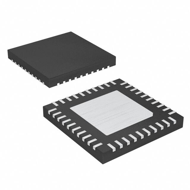


 工商网监
湘ICP备2023018690号
工商网监
湘ICP备2023018690号
