TPS54010-EP
www.ti.com
SLVSBN3 – JANUARY 2013
2.2-V to 4-V, 14-A OUTPUT SYNCHRONOUS BUCK PWM SWITCHER
WITH INTEGRATED FETs (SWIFT™)
Check for Samples: TPS54010-EP
FEATURES
1
•
•
2
•
•
•
•
•
•
•
Separate Low-Voltage Power Bus
8-mΩ MOSFET Switches for High Efficiency at
14-A Continuous Output
Adjustable Output Voltage Down to 0.9 V
Externally Compensated With 1% Internal
Reference Accuracy
Fast Transient Response
Wide PWM Frequency: Adjustable 280 kHz to
700 kHz
Load Protected by Peak Current Limit and
Thermal Shutdown
Integrated Solution Reduces Board Area and
Total Cost
SWIFT Documentation, Application Notes, and
Design Software: www.ti.com/swift
APPLICATIONS
•
•
•
Low-Voltage, High-Density Systems With
Power Distributed at 2.5 V, 3.3 V Available
Point of Load Regulation for HighPerformance DSPs, FPGAs, ASICs, and
Microprocessors
Broadband, Networking, and Optical
Communications Infrastructure
SUPPORTS DEFENSE, AEROSPACE,
AND MEDICAL APPLICATIONS
•
•
•
•
•
•
•
Controlled Baseline
One Assembly and Test Site
One Fabrication Site
Available in Military (–55°C to 125°C)
Temperature Range
Extended Product Life Cycle
Extended Product-Change Notification
Product Traceability
DESCRIPTION
As a member of the SWIFT™ family of dc/dc regulators, the TPS54010 low-input voltage, high-output current
synchronous buck PWM converter integrates all required active components. Included on the substrate with the
listed features are a true, high- performance, voltage error amplifier that enables maximum performance under
transient conditions and flexibility in choosing the output filter L and C components; an undervoltage-lockout
circuit to prevent start-up until the VIN input voltage reaches 3 V; an internally and externally set slowstart circuit
to limit in-rush currents; and a power-good output useful for processor/logic reset, fault signaling, and supply
sequencing.
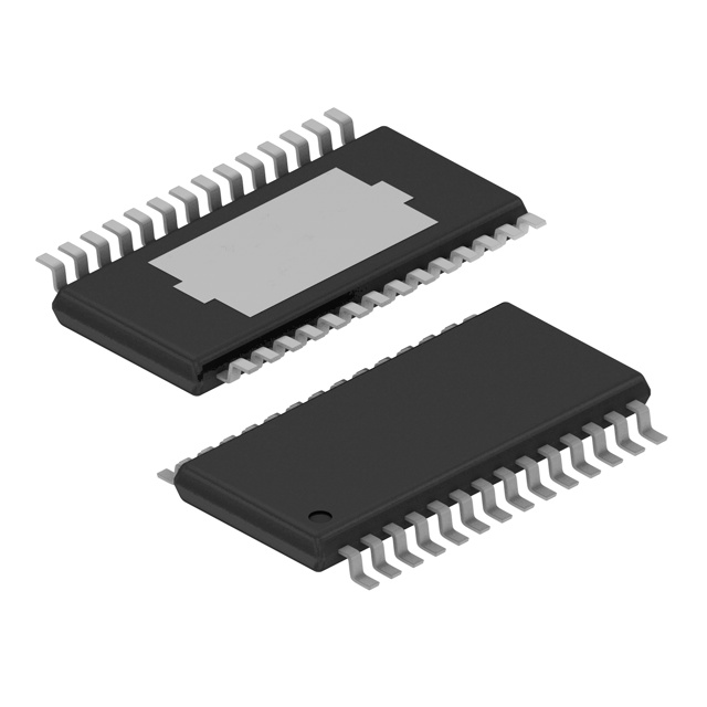
The TPS54010 is available in a thermally enhanced 28-pin TSSOP (PWP) PowerPAD™ package, which
eliminates bulky heatsinks.
1
2
Please be aware that an important notice concerning availability, standard warranty, and use in critical applications of
Texas Instruments semiconductor products and disclaimers thereto appears at the end of this data sheet.
SWIFT, PowerPAD are trademarks of Texas Instruments.
PRODUCTION DATA information is current as of publication date.
Products conform to specifications per the terms of the Texas
Instruments standard warranty. Production processing does not
necessarily include testing of all parameters.
Copyright © 2013, Texas Instruments Incorporated
�TPS54010-EP
SLVSBN3 – JANUARY 2013
www.ti.com
SIMPLIFIED SCHEMATIC
2.5 V or 3.3 V
Input1
EFFICIENCY
vs
OUTPUT CURRENT
0.68 mH
PVIN
350 mF
PH
TPS54010
BOOT
PGND
Output
100
0.047 mF
200 mF
0.1 mF
95
90
3.3 V
VIN
1 mF
COMP
VBIAS
AGND VSENSE
85
120 pF
4.64 kW
10 kW
3300 pF
422 W
1 mF
Efficiency − %
Input2
80
75
70
65
14.7 kW
1500 pF
Compensation
Network
VIN = 3.3 V,
PVIN = 2.5 V,
VO = 1.5 V,
fs= 700 kHz
60
55
50
0
2
4
6
8
10
12
14
16
IO − Output Current − A
2
Submit Documentation Feedback
Copyright © 2013, Texas Instruments Incorporated
Product Folder Links: TPS54010-EP
�TPS54010-EP
www.ti.com
SLVSBN3 – JANUARY 2013
This integrated circuit can be damaged by ESD. Texas Instruments recommends that all integrated circuits be handled with
appropriate precautions. Failure to observe proper handling and installation procedures can cause damage.
ESD damage can range from subtle performance degradation to complete device failure. Precision integrated circuits may be more
susceptible to damage because very small parametric changes could cause the device not to meet its published specifications.
ORDERING INFORMATION (1)
TJ
–55°C to 125°C
(1)
OUTPUT VOLTAGE
Adjustable down to 0.9 V
PACKAGE
Plastic HTSSOP (PWP)
ORDERABLE PART NUMBER
VID NUMBER
TPS54010MPWPREP
V62/13604-01XE
TPS54010MPWPEP
V62/13604-01XE-T
For the most current package and ordering information, see the Package Option Addendum at the end of this document, or see the TI
web site at www.ti.com.
ABSOLUTE MAXIMUM RATINGS
over operating free-air temperature range (unless otherwise noted)
(1)
TPS54010
VI
Input voltage range
VO
Output voltage range
VO
Source current
IS
Sink current
SS/ENA, SYNC
–0.3 to 7
RT
–0.3 to 6
VSENSE
–0.3 to 4
PVIN, VIN
–0.3 to 4.5
BOOT
–0.3 to 10
VBIAS, COMP, PWRGD
–0.3 to 7
PH
–0.6 to 6
V
V
PH
Internally limited
COMP, VBIAS
6
PH
25
A
COMP
6
mA
SS/ENA, PWRGD
Voltage differential
UNIT
mA
10
AGND to PGND
±0.3
V
TJ
Junction temperature range
–55 to 150
°C
Tstg
Storage temperature range
–65 to 150
°C
Lead temperature 1,6 mm (1/16 inch) from case for 10 seconds
Electrostatic Discharge (ESD) ratings
(1)
300
°C
Human body model (HBM)
1.5
kV
CDM
750
V
Stresses beyond those listed under “absolute maximum ratings” may cause permanent damage to the device. These are stress ratings
only, and functional operation of the device at these or any other conditions beyond those indicated under “recommended operating
conditions” is not implied. Exposure to absolute-maximum-rated conditions for extended periods may affect device reliability.
RECOMMENDED OPERATING CONDITIONS
MIN
VI
TJ
Input voltage, VIN
NOM
MAX
UNIT
3
4
Power Input voltage, PVIN
2.2
4
V
Operating junction temperature
–55
125
°C
Submit Documentation Feedback
Copyright © 2013, Texas Instruments Incorporated
Product Folder Links: TPS54010-EP
V
3
�TPS54010-EP
SLVSBN3 – JANUARY 2013
www.ti.com
THERMAL INFORMATION
TPS54010
THERMAL METRIC (1)
PWP
UNITS
28 PINS
Junction-to-ambient thermal resistance (2)
θJA
30.5
(3)
θJCtop
Junction-to-case (top) thermal resistance
θJB
Junction-to-board thermal resistance (4)
11.6
ψJT
Junction-to-top characterization parameter (5)
0.4
ψJB
Junction-to-board characterization parameter (6)
11.4
θJCbot
Junction-to-case (bottom) thermal resistance (7)
0.9
(1)
(2)
(3)
(4)
(5)
(6)
(7)
13.5
°C/W
For more information about traditional and new thermal metrics, see the IC Package Thermal Metrics application report, SPRA953.
The junction-to-ambient thermal resistance under natural convection is obtained in a simulation on a JEDEC-standard, high-K board, as
specified in JESD51-7, in an environment described in JESD51-2a.
The junction-to-case (top) thermal resistance is obtained by simulating a cold plate test on the package top. No specific JEDECstandard test exists, but a close description can be found in the ANSI SEMI standard G30-88.
The junction-to-board thermal resistance is obtained by simulating in an environment with a ring cold plate fixture to control the PCB
temperature, as described in JESD51-8.
The junction-to-top characterization parameter, ψJT, estimates the junction temperature of a device in a real system and is extracted
from the simulation data for obtaining θJA, using a procedure described in JESD51-2a (sections 6 and 7).
The junction-to-board characterization parameter, ψJB, estimates the junction temperature of a device in a real system and is extracted
from the simulation data for obtaining θJA , using a procedure described in JESD51-2a (sections 6 and 7).
The junction-to-case (bottom) thermal resistance is obtained by simulating a cold plate test on the exposed (power) pad. No specific
JEDEC standard test exists, but a close description can be found in the ANSI SEMI standard G30-88.
Spacer
ELECTRICAL CHARACTERISTICS
TJ = -55°C to 125°C, VIN = 3 V to 4 V, PVIN = 2.2 V to 4 V (unless otherwise noted)
PARAMETER
TEST CONDITIONS
MIN
TYP
MAX
UNIT
SUPPLY VOLTAGE, VIN
VI
Input voltage, VIN
Supply voltage range, PVIN
3
4
V
2.2
4
V
6.3
10
mA
8.3
13
mA
SHUTDOWN, SS/ENA = 0 V, PVIN = 2.5 V
1
1.4
mA
fs = 350 kHz, RT open, PH pin open, PVIN = 3.3 V,
SYNC = 0 V
6
8
mA
fs = 550 kHz, RT open, PH pin open, SYNC ≥ 2.5 V,
PVIN = 2.5 V, VIN = 3.3 V
6
10
mA
Output = 1.8 V
fs = 350 kHz, RT open, PH pin open, PVIN = 2.5 V,
SYNC = 0 V
fs = 550 kHz, RT open, PH pin open, SYNC ≥ 2.5 V,
PVIN = 2.5 V
VIN
IQ
Quiescent current
PVIN
SHUTDOWN, SS/ENA = 0 V, VIN = 3.3 V
90% Vref, otherwise PWRGD is low. Note that
output is low when SS/ENA is low or the internal shutdown signal is active.
RT
28
Frequency setting resistor input. Connect a resistor from RT to AGND to set the switching frequency, fs.
SS/ENA
26
Slow-start/enable input/output. Dual function pin which provides logic input to enable/disable device
operation and capacitor input to externally set the start-up time.
SYNC
27
Synchronization input. Dual function pin which provides logic input to synchronize to an external oscillator
or pin select between two internally set switching frequencies. When used to synchronize to an external
signal, a resistor must be connected to the RT pin.
VBIAS
25
Internal bias regulator output. Supplies regulated voltage to internal circuitry. Bypass VBIAS pin to AGND
pin with a high-quality, low-ESR 0.1-µF to 1.0-µF ceramic capacitor.
VIN
24
Input supply for the internal control circuits. Bypass the VIN pin to the PGND pins close to device package
with a high-quality, low-ESR 1-µF ceramic capacitor.
VSENSE
2
Error amplifier inverting input. Connect to output voltage compensation network/output divider.
PVIN
6
Submit Documentation Feedback
Copyright © 2013, Texas Instruments Incorporated
Product Folder Links: TPS54010-EP
�TPS54010-EP
www.ti.com
SLVSBN3 – JANUARY 2013
Figure 1. FUNCTIONAL BLOCK DIAGRAM
VBIAS
AGND
VIN
SS/ENA
Falling
Edge
Deglitch
1.2 V
Hysteresis: 0.03 V
2.5 µs
VIN UVLO
Comparator
VIN
2.95 V
Hysteresis: 0.11 V
VIN
REG
VBIAS
Enable
Comparator
3.0 − 4.0 V
SHUTDOWN
PVIN
ILIM
Comparator
Thermal
Shutdown
150°C
2.2 − 4.0 V
Leading
Edge
Blanking
Falling
and
Rising
Edge
Deglitch
100 ns
BOOT
8 mΩ
2.5 µs
SS_DIS
SHUTDOWN
Internal/External
Slow-start
(Internal Slow-start Time = 3.35 ms
PH
+
−
R Q
Error
Amplifier
Reference
VREF = 0.891 V
S
PWM
Comparator
LOUT
VO
CO
Adaptive Dead-Time
and
Control Logic
VIN
8 mΩ
OSC
PGND
Power-Good
Comparator
PWRGD
VSENSE
Falling
Edge
Deglitch
0.90 Vref
TPS54010
Hysteresis: 0.03 Vref
VSENSE
COMP
SHUTDOWN
35 µs
RT SYNC
Submit Documentation Feedback
Copyright © 2013, Texas Instruments Incorporated
Product Folder Links: TPS54010-EP
7
�TPS54010-EP
SLVSBN3 – JANUARY 2013
www.ti.com
TYPICAL CHARACTERISTICS
DRAIN-SOURCE ON-STATE
RESISTANCE
vs
JUNCTION TEMPERATURE
INTERNALLY SET OSCILLATOR
FREQUENCY
vs
JUNCTION TEMPERATURE
8
6
4
2
0
750
f − Externally Set Oscillator Frequency − kHz
VIN = 3.3 V,
PVIN = 2.5 V,
IO = 9 A
650
SYNC ³ 2.5 V
550
450
SYNC £ 0.8 V
350
250
−55 −40 −20
0
20
40
60
80
100
−55 −40 −20
125
TJ − Junction Temperature − °C
0
20
40
60
80
100
800
RT = 68kΩ
700
600
RT = 100kΩ
500
400
RT = 180kΩ
300
200
−55 −40 −20
125
TJ − Junction Temperature − °C
0
20
40
60
80
100
Figure 2.
Figure 3.
Figure 4.
VOLTAGE REFERENCE
vs
JUNCTION TEMPERATURE
DEVICE POWER DISSIPATION
vs
OUTPUT CURRENT
REFERENCE VOLTAGE
vs
INPUT VOLTAGE
0.895
0.895
8
VO = 1.5 V,
VI = PVIN = 3.3 V,
TJ = 125°C
7
Device Power Dissipation − W
Vref − Voltage Reference − V
0.893
0.891
0.889
0.887
125
TJ − Junction Temperature − °C
VO − Output Voltage Regulation − V
10
f − Internally Set Oscillator Frequency − kHz
Drain-Source On-State Resistance − Ω
12
EXTERNALLY SET OSCILLATOR
FREQUENCY
vs
JUNCTION TEMPERATURE
6
5
4
3
2
PVIN = 2.5 V
0.893
0.891
0.889
0.887
1
0.885
0
0.885
−55 −40 −20
0
20
40
60
80
100
125
0
TJ − Junction Temperature − °C
Figure 5.
IO − Output Current − A
3.2
3.3
3.4
VI − Input Voltage − V
Figure 6.
Figure 7.
5
10
15
−20
3.65
−40
Gain − dB
−60
80
Phase
−80
−100
60
−120
40
Gain
20
−140
−160
0
−180
−20
1
10
100
−200
1 k 10 k 100 k 1 M 10 M
Phase − Degrees
100
Internal Slow-Start Time − ms
120
3.6
VIN = 3.3 V,
PVIN = 2.5 V
3.50
3.35
3.20
3.05
2.90
2.75
f − Frequency − Hz
−55 −40 −20
0
20
40
60
80
100
125
TJ − Junction Temperature − °C
Figure 8.
8
3.5
3.80
0
RL = 10 kΩ,
CL = 160 pF,
TA = 25°C
3.1
INTERNAL SLOW-START TIME
vs
JUNCTION TEMPERATURE
ERROR AMPLIFIER
OPEN-LOOP RESPONSE
140
3
20
Figure 9.
Submit Documentation Feedback
Copyright © 2013, Texas Instruments Incorporated
Product Folder Links: TPS54010-EP
�TPS54010-EP
www.ti.com
SLVSBN3 – JANUARY 2013
APPLICATION INFORMATION
PCB LAYOUT
ANALOG GROUND TRACE
FREQUENCY SET RESISTOR
AGND
RT
VSENSE
COMPENSATION
NETWORK
COMP
SYNC
INPUT
BYPASS
CAPACITOR
SLOW-START
CAPACITOR
SS/ENA
BIAS CAPACITOR
PWRGD
BOOT
CAPACITOR
BOOT
VIN
PH
EXPOSED
POWERPAD PVIN
AREA
PVIN
PH
PVIN
PH
PVIN
PH
PGND
PH
VOUT
PH
VBIAS
PVIN
OUTPUT INDUCTOR
PGND
OUTPUT
FILTER
CAPACITOR
PGND
PGND
PGND
INPUT
BYPASS
CAPACITOR
INPUT
BULK
FILTER
TOPSIDE GROUND AREA
VIA to GROUND PLANE
Figure 10. TPS54010 Layout
The PVIN pins are connected together on the printedcircuit board (PCB) and bypassed with a low ESR
ceramic bypass capacitor. Care should be taken to
minimize the loop area formed by the bypass
capacitor connections, the PVIN pins, and the
TPS54010 ground pins. The minimum recommended
bypass capacitance is a 10-µF ceramic capacitor with
a X5R or X7R dielectric. The optimum placement is
as close as possible to the PVIN pins, the AGND,
and PGND pins. See Figure 10 for an example of a
board layout. If the VIN is connected to a separate
source supply, it is bypassed with its own capacitor.
There is an area of ground on the top layer of the
PCB, directly under the IC, with an exposed area for
connection to the PowerPAD. Use vias to connect
this ground area to any internal ground planes. Use
additional vias at the ground side of the input and
output filter capacitors. The AGND and PGND pins
are tied to the PCB ground by connecting them to the
ground area under the device as shown in Figure 10.
Use a separate wide trace for the analog ground
signal path. This analog ground is used for the
voltage set point divider, timing resistor RT, slow-start
capacitor, and bias capacitor grounds. The PH pins
are tied together and routed to the output inductor.
Because the PH connection is the switching node, an
inductor is located close to the PH pins, and the area
of the PCB conductor is minimized to prevent
excessive capacitive coupling. Connect the boot
capacitor between the phase node and the BOOT pin
as shown in Figure 10. Keep the boot capacitor close
to the IC, and minimize the conductor trace lengths.
Connect the output filter capacitor(s) between the
VOUT trace and PGND. It is important to keep the
loop formed by the PH pins, Lout, Cout, and PGND
as small as is practical. Place the compensation
components from the VOUT trace to the VSENSE
and COMP pins. Do not place these components too
close to the PH trace. Due to the size of the IC
package and the device pinout, they must be routed
Submit Documentation Feedback
Copyright © 2013, Texas Instruments Incorporated
Product Folder Links: TPS54010-EP
9
�TPS54010-EP
SLVSBN3 – JANUARY 2013
www.ti.com
close, but maintain as much separation as possible
while keeping the layout compact. Connect the bias
capacitor from the VBIAS pin to analog ground using
the isolated analog ground trace. If a slow-start
capacitor or RT resistor is used, or if the SYNC pin is
used to select 350-kHz operating frequency, connect
them to this trace.
For operation at full rated load current, the analog
ground plane must provide an adequate heatdissipating area. A 3-inch by 3-inch plane of 1-ounce
copper is recommended, though not mandatory,
depending on ambient temperature and airflow. Most
applications have larger areas of internal ground
plane available, and the PowerPAD must be
connected to the largest area available. Additional
areas on the top or bottom layers also help dissipate
8 PL Ø 0.0130
4 PL
Ø 0.0180
heat, and any area available must be used when 6-A
or greater operation is desired. Connection from the
exposed area of the PowerPAD to the analog ground
plane layer must be made using 0.013-inch diameter
vias to avoid solder wicking through the vias.
Eight vias must be in the PowerPAD area with four
additional vias located under the device package. The
size of the vias under the package, but not in the
exposed thermal pad area, can be increased to
0.018.
Additional vias beyond
the
twelve
recommended that enhance thermal performance
must be included in areas not under the device
package.
Minimum Recommended Thermal Vias: 8 x 0.013 Diameter Inside
PowerPAD Area 4 x 0.018 Diameter Under Device as Shown.
Additional 0.018 Diameter Vias May Be Used if Top Side Analog Ground
Area Is Extended.
Connect Pin 1 to Analog Ground Plane
in This Area for Optimum Performance
0.06
0.0150
0.0339
0.0650
0.0500
0.3820 0.3478 0.0500
0.0500
0.2090
0.0256
0.0650
0.0339
0.1700
0.1340
Minimum Recommended Top
Side Analog Ground Area
Minimum Recommended Exposed
Copper Area for PowerPAD. 5mm
Stencils May Require 10 Percent
Larger Area
0.0630
0.0400
Figure 11. Recommended Land Pattern for 28-Pin PWP PowerPAD
10
Submit Documentation Feedback
Copyright © 2013, Texas Instruments Incorporated
Product Folder Links: TPS54010-EP
�TPS54010-EP
www.ti.com
SLVSBN3 – JANUARY 2013
µF
µF
µF
kΩ
µF
kΩ
µF
µF
kΩ
µ
µF
µF
kΩ
µF
kΩ
kΩ
Figure 12. Application Circuit, 2.5 V to 1.5 V
Figure 12 shows the schematic for a typical
TPS54010 application. The TPS54010 can provide
up to 14-A output current at a nominal output voltage
of 1.5 V. Nominal input voltages are 2.5 V for PVIN
and 3.3 V for VIN. For proper thermal performance,
the exposed PowerPAD underneath the device must
be soldered down to the printed-circuit board.
•
•
•
Output ripple voltage
Output current rating
Operating frequency
For this design example, use the following as the
input parameters:
Table 1.
DESIGN PROCEDURE
The following design procedure can be used to select
component values for the TPS54010. Alternately, the
SWIFT Designer Software may be used to generate a
complete design. The SWIFT Designer Software uses
an iterative design procedure and accesses a
comprehensive database of components when
generating a design. This section presents a
simplified discussion of the design process.
DESIGN PARAMETERS
DESIGN PARAMETER
EXAMPLE VALUE
Input voltage (VIN)
3.3 V
Input voltage range (PVIN)
2.2 to 3.5 V
Output voltage
1.5 V
Input ripple voltage
300 mV
Output ripple voltage
50 mV
Output current rating
14 A
Operating frequency
700 kHz
SWITCHING FREQUENCY
To begin the design process, a few parameters must
be decided. The designer needs to know:
• Input voltage range
• Output voltage
• Input ripple voltage
The switching frequency can be set to either one of
two internally programmed frequencies or set to a
externally programmed frequency. With the RT pin
open, setting the SYNC pin at or above 2.5 V selects
550-kHz operation, whereas grounding or leaving the
Submit Documentation Feedback
Copyright © 2013, Texas Instruments Incorporated
Product Folder Links: TPS54010-EP
11
�TPS54010-EP
SLVSBN3 – JANUARY 2013
www.ti.com
SYNC pin open selects 350-kHz operation. For this
design, the switching frequency is externally
programmed using the RT pin. By connecting a
resistor (R4) from RT to AGND, any frequency in the
range of 250 to 700 kHz can be set. Use Equation 1
to determine the proper value of RT.
R4(kW) + 500 kHz 100 kW
ƒs(kHz)
(1)
In this example circuit, R4 is calculated to be 71.5 kΩ
and the switching frequency is set at 700 kHz.
INPUT CAPACITORS
This input ripple voltage can be approximated by
Equation 2:
I
PVIN
+
0.25
OUT(MAX)
) I
OUT(MAX)
C
ƒ sw
BULK
ǒ
ESR
MAX
Ǔ
(2)
Where IOUT(MAX) is the maximum load current.
The TPS54010 requires an input de-coupling
capacitor and, depending on the application, a bulk
input capacitor. ƒsw is the switching frequency, C(BULK)
is the bulk capacitor value and ESRMAX is the
maximum series resistance of the bulk capacitor.
The maximum RMS ripple current also needs to be
checked. For worst-case conditions, this can be
approximated by Equation 3:
I
OUT(MAX)
I
+
CIN
2
(3)
In this case, the input ripple voltage would be 155 mV
and the RMS ripple current would be 7 A. The
maximum voltage across the input capacitors would
be Vin max plus delta Vin/2. The chosen bulk
capacitor, a Sanyo POSCAP 6TPD330M is rated for
6.3 V and 4.4 A of ripple current; two bypass
capacitors, TDK C3225X5R1C106M are each rated
12
OUTPUT FILTER COMPONENTS
Two components need to be selected for the output
filter, L1 and C2. Because the TPS54010 is an
externally compensated device, a wide range of filter
component types and values can be supported.
Inductor Selection
The TPS54010 requires an input de-coupling
capacitor and, depending on the application, a bulk
input capacitor. The minimum value for the decoupling capacitor, C9, is 10 µF. A high-quality
ceramic type X5R or X7R is recommended. The
voltage rating should be greater than the maximum
input voltage. Additionally, some bulk capacitance
may be needed, especially if the TPS54010 circuit is
not located within about 2 inches from the input
voltage source. The value for this capacitor is not
critical but it also should be rated to handle the
maximum input voltage including ripple voltage, and
should filter the output so that input ripple voltage is
acceptable.
DV
for 16 V, and the ripple current capacity is greater
than 3 A at the operating frequency of 700 kHz. Total
ripple current handling is in excess of 10.4 A. It is
important that the maximum ratings for voltage and
current are not exceeded under any circumstance.
To calculate the minimum value of the output
inductor, use Equation 4
V
L
+
MIN
V
ǒVin(MAX) * VOUTǓ
OUT
IN(MAX)
K
IND
I
OUT
F sw
(4)
KIND is a coefficient that represents the amount of
inductor ripple current relative to the maximum output
current. For designs using low ESR output capacitors
such as ceramics, use KIND = 0.3. When using higher
ESR output capacitors, KIND = 0.2 yields better
results.
For this design example, use KIND = 0.2 to keep the
inductor ripple current small. The minimum inductor
value is calculated to be 0.44 µH.
For the output filter inductor, it is important that the
RMS current and saturation current ratings not be
exceeded. The RMS inductor current can be found
from Equation 5:
I
L(RMS)
+
Ǹ
I
) 1
OUT(MAX) 12
2
ȡ
ȧVOUT
Ȣ
ǒVin(MAX) * VOUTǓ
V
IN(MAX)
L
OUT
F sw
2
ȣ
0.8ȧ
Ȥ
(5)
and the peak inductor current can be found from
Equation 6
V
I
L(PK)
+I
OUT(MAX)
)
OUT
1.6 V
ǒVin(MAX) * VOUTǓ
IN(MAX)
L
OUT
F sw
(6)
For this design, the RMS inductor current is 15.4 A,
and the peak inductor current is 15.1 A. For this
design, a Vishay IHLP2525CZ-01 style output
inductor is specified. The largest value greater than
0.44 µH that meets these current requirements is
0.68 µH. Increasing the inductor value decreases the
ripple current and the corresponding output ripple
voltage. The inductor value can be decreased if more
margin in the RMS current is required. In general,
inductor values for use with the TPS54010 falls in the
range of 0.47 to 2.2 µH.
Submit Documentation Feedback
Copyright © 2013, Texas Instruments Incorporated
Product Folder Links: TPS54010-EP
�TPS54010-EP
www.ti.com
SLVSBN3 – JANUARY 2013
Capacitor Requirements
The important design factors for the output capacitor
are dc voltage rating, ripple current rating, and
equivalent series resistance (ESR). The dc voltage
and ripple current ratings cannot be exceeded. The
ESR is important because along with the inductor
current it determines the amount of output ripple
voltage. The actual value of the output capacitor is
not critical, but some practical limits do exist.
Consider the relationship between the desired closedloop crossover frequency of the design and LC corner
frequency of the output filter. In general, it is desirable
to keep the closed-loop crossover frequency at less
than 1/5 of the switching frequency. With high
switching frequencies such as the 500 kHz frequency
of this design, internal circuit limitations of the
TPS54010 limit the practical maximum crossover
frequency to about 70 kHz. To allow for adequate
phase gain in the compensation network, the LC
corner frequency should be about one decade or so
below the closed-loop crossover frequency. This
limits the minimum capacitor value for the output filter
to:
C
OUT(MIN)
+
1
L
OUT
ǒ
K
2p ƒ
CO
Ǔ
2
(7)
Where K is the frequency multiplier for the spread
between fLC and fCO. K should be between 5 and 15,
typically 10 for one decade difference. For a desired
crossover of 100-kHz and a 0.68-µH inductor, the
minimum value for the output capacitor is 93 µF using
a minimum K factor of 5. Increasing the K factor
would require using a larger capacitance as 100 kHz
is approaching the maximum practical closed-loop
crossover frequency for this device. The selected
output capacitor must be rated for a voltage greater
than the desired output voltage plus one half the
ripple voltage. Any de-rating amount must also be
included. The maximum RMS ripple current in the
output capacitors is given by Equation 8:
I
+ 1
COUT(RMS)
Ǹ12
ȡVOUT ǒVPVIN(MAX) * VOUTǓȣ
ȧ V
L
F sw ȧ
PVIN(MAX)
OUT
Ȣ
Ȥ
(8)
The calculated RMS ripple current is 780 mA in the
output capacitors.
The maximum ESR of the output capacitor is
determined by the amount of allowable output ripple
as specified in the initial design parameters. The
output ripple voltage is the inductor ripple current
times the ESR of the output filter; therefore, the
maximum specified ESR as listed in the capacitor
data sheet is given by Equation 9 :
ESR
MAX
+N
C
ȡVIN(MAX) LOUT F sw 0.8ȣ
ȧ
ȧ
Ȣ VOUT ǒVIN(MAX) * VOUTǓ Ȥ
DV
P*P(MAX)
(9)
and the maximum ESR required is 22.2 mΩ. A
capacitor that meets these requirements is a Cornell
Dubilier Special Polymer (SP) ESRD101M06 rated at
6.3 V with a maximum ESR of 0.015 Ω and a ripple
current rating of 2 A. An additional small 0.1-µF
ceramic bypass capacitor C13 is a also used.
Other capacitor types work well with the TPS54010,
depending on the needs of the application.
Compensation Components
The external compensation used with the TPS54010
allows for a wide range of output filter configurations.
A large range of capacitor values and types of
dielectric are supported. The design example uses
Type-3 compensation consisting of R1, R3, R5, C6,
C7, and C8. Additionally, R2 along with R1 forms a
voltage divider network that sets the output voltage.
These component reference designators are the
same as those used in the SWIFT Designer
Software. There are a number of different ways to
design a compensation network. This procedure
outlines a relatively simple procedure that produces
good results with most output filter combinations. Use
the SWIFT Designer Software for designs with
unusually high closed-loop crossover frequencies,
low value, low ESR output capacitors such as
ceramics or if you are unsure about the design
procedure.
When designing compensation networks for the
TPS54010, a number of factors need to be
considered. The gain of the compensated error
amplifier should not be limited by the open-loop
amplifier gain characteristics and should not produce
excessive gain at the switching frequency. Also, the
closed-loop crossover frequency should be set less
than one-fifth of the switching frequency, and the
phase margin at crossover must be greater than 45
degrees. The general procedure outlined here
produces results consistent with these requirements
without going into great detail about the theory of loop
compensation.
First, calculate the output filter LC corner frequency
using Equation 10:
1
ƒ
+
LC
2p L
C
OUT OUT
(10)
Ǹ
For the design example, fLC = 19.3 kHz.
Submit Documentation Feedback
Copyright © 2013, Texas Instruments Incorporated
Product Folder Links: TPS54010-EP
13
�TPS54010-EP
SLVSBN3 – JANUARY 2013
www.ti.com
The closed-loop crossover frequency should be
chosen to be greater than fLC and less than one-fifth
of the switching frequency. Also, the crossover
frequency should not exceed 150 kHz, as the error
amplifier may not provide the desired gain. For this
design, a crossover frequency of 100 kHz was
chosen. This value is chosen for comparatively wide
loop bandwidth while still allowing for adequate phase
boost to insure stability.
Next, calculate the R2 resistor value for the output
voltage of 1.5 V using Equation 11:
R2 + R1 0.891
V
* 0.891
OUT
(11)
For any TPS54010 design, start with an R1 value of
10 kΩ. R2 is 14.7 kΩ.
Now, the values for the compensation components
that set the poles and zeros of the compensation
network can be calculated. Assuming that R1 >> than
R5 and C6 >> C7, the pole and zero locations are
given by Equation 12 through Equation 18:
1
ƒ +
Z1
2pR3C6
(12)
1
ƒ +
Z2
2pR1C8
(13)
1
ƒ
+
P1
2pR5C8
(14)
1
ƒ
+
P2
2pR3C7
(15)
Additionally, there is a pole at the origin, which has
unity gain at a frequency:
1
ƒ
+
INT
2pR1C6
(16)
This pole is used to set the overall gain of the
compensated error amplifier and determines the
closed-loop crossover frequency. Because R1 is
given as 1 kΩ and the crossover frequency is
selected as 100 kHz, the desired fINT can be
calculated from Equation 17:
ƒ
CO
ƒ
+
INT
V
2
IN(MAX)
(17)
And the value for C6 is given by Equation 18:
1
C6 +
2pR1 ƒ
INT
(18)
The first zero, fZ1 is located at one-half the output
filter LC corner frequency; so, R3 can be calculated
from:
1
R3 +
pC6 ƒ
LC
(19)
14
The second zero, fZ2 is located at the output filter LC
corner frequency; so, C8 can be calculated from:
1
C8 +
2pR1 ƒ
LC
(20)
The first pole, fP1 is located to coincide with output
filter ESR zero frequency. This frequency is given by:
1
ƒ
+
ESR0
2pR
C
ESR OUT
(21)
where RESR is the equivalent series resistance of the
output capacitor.
In this case, the ESR zero frequency is 88.4 kHz, and
R5 can be calculated from:
1
R5 +
2pC8 ƒ
ESR
(22)
The final pole is placed at a frequency above the
closed-loop crossover frequency high enough to not
cause the phase to decrease too much at the
crossover frequency while still providing enough
attenuation so that there is little or no gain at the
switching frequency. The fP2 pole location for this
circuit is set to 3.5 times the closed-loop crossover
frequency and the last compensation component
value C7 can be derived:
1
C7 +
7pR3 ƒ
CO
(23)
Note that capacitors are only available in a limited
range of standard values, so the nearest standard
value has been chosen for each capacitor. The
measured closed-loop response for this design is
shown in Figure 5.
BIAS AND BOOTSTRAP CAPACITORS
Every TPS54010 design requires a bootstrap
capacitor, C3, and a bias capacitor, C4. The
bootstrap capacitor must be a 0.1 µF. The bootstrap
capacitor is located between the PH pins and BOOT.
The bias capacitor is connected between the VBIAS
pin and AGND. The value should be 1.0 µF. Both
capacitors should be high-quality ceramic types with
X7R or X5R grade dielectric for temperature stability.
They should be placed as close to the device
connection pins as possible.
POWER GOOD
The TPS54010 is provided with a power-good output
pin PWRGD. This output is an open-drain output and
is intended to be pulled up to a 3.3-V or 5-V logic
supply. A 10-kΩ pullup works well in this application.
Submit Documentation Feedback
Copyright © 2013, Texas Instruments Incorporated
Product Folder Links: TPS54010-EP
�TPS54010-EP
www.ti.com
SLVSBN3 – JANUARY 2013
SNUBBER CIRCUIT
R10 and C11 of the application schematic comprise a
snubber circuit. The snubber is included to reduce
overshoot and ringing on the phase node when the
internal high-side FET turns on. Because the
frequency and amplitude of the ringing depends to a
µ
µ
µ
large degree on parasitic effects, it is best to choose
these component values based on actual
measurements of any design layout. See literature
number SLUP100 for more detailed information on
snubber design.
kΩ
µ
71.5 kΩ
µF
µF
kΩ
µ
µF
µF
Ω
14.7 kΩ
µF
10 kΩ
The following part numbers are used for test purposes:
C1 = T520D337M0O4ASE015 (Kemet)
C2 = TDK C3225X5R0J107M ceramic 6.3 V X5R
L1 = IHLP2525CZ−01 0.68 µH (Vishay Dale)
Figure 13. 1.5-V Power Supply With Ceramic Output Capacitors
Figure 13 shows an application where all ceramic
capacitors, including the main output filter capacitor,
are used. The compensation network components
were calculated using SWIFT Designer Software. See
Figure 22 through Figure 30 for loop response,
performance graphs, and switching waveforms for
this circuit.
Submit Documentation Feedback
Copyright © 2013, Texas Instruments Incorporated
Product Folder Links: TPS54010-EP
15
�TPS54010-EP
SLVSBN3 – JANUARY 2013
µF
www.ti.com
µF
µF
kΩ
µF
µ
µF
10 kΩ
µF
µF
µF
20 kΩ
10 kΩ
10 kΩ
2 kΩ
10 kΩ
14.7 kΩ
10 kΩ
49.9 Ω
10 kΩ
49.9 Ω
µF
Figure 14. 1.5-V Power Supply With Remote Sense
With an output current of 14 A, if the load is located
far from the dc/dc converter circuit, it may be
beneficial to include a remote sense capability.
Figure 14 is an example of a power supply
incorporating active differential remote sensing. As
the TPS54010 only has a positive VSENSE input, this
circuit compensates for voltage drops in both the
output voltage rail and the return (GND). The
16
difference amplifier of U2 forces the output of the
TPS54010 to generate an output voltage that
maintains a constant 1.5-V difference between
+1.5V_REMOTE_SENSE
and
1.5V_REMOTE_SENSE.
Submit Documentation Feedback
Copyright © 2013, Texas Instruments Incorporated
Product Folder Links: TPS54010-EP
�TPS54010-EP
www.ti.com
SLVSBN3 – JANUARY 2013
3.6 V
100 nF
330 µF
10 µF
10 µF
C17
1 µF
100 nF
0.047 µF
1 µF
10 kΩ
0.68 µH
0.047 µF
2.4 kΩ
100 µF
100 µF
0.1 µF
422 Ω
14.7 kΩ
10 kΩ
Figure 15. 2.5 V to 1.5 V Power Supply with Charge Pump
If a suitable 3-V to 4-V source is not available for the VIN supply, a charge pump may be used to boost the PVIN
voltage. In this circuit, the charge pump is used to boost a 2.5-V source to a nominal 3.6 V.
Submit Documentation Feedback
Copyright © 2013, Texas Instruments Incorporated
Product Folder Links: TPS54010-EP
17
�TPS54010-EP
SLVSBN3 – JANUARY 2013
www.ti.com
PERFORMANCE GRAPHS
The performance data for Figure 16 through Figure 24 are for the circuit in Figure 12. Conditions are PVIN = 2.5
V, VIN = 3.3 V, VO = 1.5 V, fs = 700 kHz, and IO = 7 A, TA = 25°C, unless otherwise specified.
MEASURED LOOP RESPONSE
vs
FREQUENCY
180
40
Gain - dB
20
60
Gain
0
0
-20
-60
-40
-120
Phase - Degrees
120
Output Voltage Variation - %
Phase
LINE REGULATION
vs
INPUT VOLTAGE
0.5
0.3
0.4
0.25
0.3
Output Voltage Deviation - %
60
LOAD REGULATION
vs
OUTPUT CURRENT
3.3 V
0.2
2.5 V
0.1
0
2.2 V
-0.1
-0.2
4.0 V
-0.3
-0.4
-60
100
1k
10 k
100 k
f - Frequency - Hz
-180
1M
Figure 16.
2
4
6
8
10
IO - Output - A
12
14
PVIN(RIPPLE) = 100 mV/div (ac coupled)
2.2 V
0.1
IO = 7A
0.05
0
-0.05
IO = 14A
-0.1
-0.15
-0.2
16
-0.3
2
2.5
3
PVIN - V
3.5
4
Figure 18.
OUTPUT VOLTAGE RIPPLE
VO(RIPPLE) = 20 mV/div (ac coupled)
3.3 V
90
2.5 V
85
Efficiency - %
0
INPUT RIPPLE VOLTAGE
100
IO = 0A
-0.25
Figure 17.
EFFICIENCY
vs
OUTPUT CURRENT
95
-0.5
0.2
0.15
80
75
4.0 V
70
65
60
55
50
IO = 14 A
0
2
4
6
8
10
IO - Output - A
12
14
16
Figure 19.
LOAD TRANSIENT RESPONSE
VO = 50 mV/div (ac coupled)
V(PH) = 1 V/div
IO = 14 A
V(PH ) = 1 V/div
Time = 500 nsec/div
Time = 500 nsec/div
Figure 20.
Figure 21.
START-UP WAVEFORM
OUTPUT VOLTAGE RELATIVE
TO ENABLE
V(SS/ENA) = 1 V/div
START-UP WAVEFORM
OUTPUT VOLTAGE RELATIVE
TO VIN
VIN = 1 V/div
IO = 5 A/div
VO = 1 V/div
18
VO = 1 V/div
Time = 200 �sec/div
Time = 10 msec/div
Time = 10 msec/div
Figure 22.
Figure 23.
Figure 24.
Submit Documentation Feedback
Copyright © 2013, Texas Instruments Incorporated
Product Folder Links: TPS54010-EP
�TPS54010-EP
www.ti.com
SLVSBN3 – JANUARY 2013
PERFORMANCE GRAPHS
The performance data for Figure 25 through Figure 34 are for the circuit in Figure 13. Conditions are PVIN = 2.5
V, VIN = 3.3 V, VO = 1.5 V, fs = 700 kHz, and IO = 7 A, TA = 25°C, unless otherwise specified.
FREE-AIR TEMPERATURE
vs
MAXIMUM OUTPUT CURRENT
MEASURED LOOP RESPONSE
vs
FREQUENCY
60
125
VO = 1.5 V,
PVIN = VI = 3.3 V,
TJ = 125°C
0.4
40
120
20
85
75
65
55
60
Gain
0
0
-20
-60
-40
-120
45
Safe Operating Area
35
Phase - Degrees
95
0.3
3.3 V
0.2
2.5 V
0.1
0
2.2 V
-0.1
-0.2
4.0 V
-0.3
-0.4
25
15
0 1 2 3 4 5 6 7 8 9 10 11 12 13 14 15
-60
100
1k
10 k
100 k
f - Frequency - Hz
-180
1M
IO − Output Current − A
Note: Figure 25 applies to the application circuit
(Figure 13) installed on a 3 inch x 3 inch x 0.062 inch
four-layer PCB.
Figure 25.
Figure 26.
LINE REGULATION
vs
PVIN
EFFICIENCY
vs
OUTPUT CURRENT
0.3
-0.5
0
2
4
6
8
10 12
IO - Output Current - A
14
16
Figure 27.
INPUT RIPPLE VOLTAGE
100
PVIN(RIPPLE) = 100 mV/div (ac coupled)
2.2 V
0.25
95
0.2
IO = 0A
3.3 V
90
0.15
2.5 V
85
0.1
0.05
Efficiency - %
Output Voltage Deviation - %
0.5
Output Voltage Variation - %
105
180
Phase
Gain - dB
TA − Free-Air Temperature − ° C
115
LOAD REGULATION
vs
OUTPUT CURRENT
IO = 7A
0
-0.05
IO = 14A
-0.1
80
75
4.0 V
70
65
-0.15
60
-0.2
55
-0.25
-0.3
2
2.5
3
PVIN - V
3.5
4
Figure 28.
50
IO = 14 A
0
2
4
6
8
10 12
IO - Output Current - A
14
Figure 29.
16
V(PH) = 1 V/div
Time = 500 nsec/div
Figure 30.
Submit Documentation Feedback
Copyright © 2013, Texas Instruments Incorporated
Product Folder Links: TPS54010-EP
19
�TPS54010-EP
SLVSBN3 – JANUARY 2013
www.ti.com
PERFORMANCE GRAPHS (continued)
OUTPUT VOLTAGE RIPPLE
LOAD TRANSIENT RESPONSE
VO = 100 mV/div (ac coupled)
VO(RIPPLE) = 10 mV/div (ac coupled)
START-UP WAVEFORM
OUTPUT VOLTAGE RELATIVE
TO ENABLE
V(SS/ENA) = 1 V/div
IO = 5 A/div
VO = 1 V/div
IO = 14 A
V(PH ) = 1 V/div
Time = 500 nsec/div
Time = 200 msec/div
Time = 10 msec/div
Figure 31.
Figure 32.
Figure 33.
START-UP WAVEFORM
OUTPUT VOLTAGE RELATIVE
TO ENABLE
VIN = 1 V/div
VO = 1 V/div
Time = 10 msec/div
Figure 34.
DETAILED DESCRIPTION
OPERATING WITH SEPARATE PVIN
The TPS54010 is designed to operate with the power stage (high-side and low-side MOSFETs) and the PVIN
input connected to a separate power source from VIN. The primary intended application has VIN connected to a
3.3-V bus and PVIN connected to a 2.5-V bus. The TPS54010 cannot be damaged by any sequencing of these
voltages. However, the UVLO (see detailed description section) is referenced to the VIN input. Some conditions
may cause undesirable operation.
If PVIN is absent when the VIN input is high, the slow-start is released, and the PWM circuit goes to maximum
duty factor. When the PVIN input ramps up, the output of the TPS54010 follows the PVIN input until enough
voltage is present to regulate to the proper output value.
NOTE
If the PVIN input is controlled via a fast bus switch, it results in a hard-start condition and may damage the load
(i.e., whatever is connected to the regulated output of the TPS54010). If a power-good signal is not available
from the 2.5-V power supply, one can be generated using a comparator and hold the SS/ENA pin low until the
2.5-V bus power is good. An example of this is shown in Figure 35. This circuit can also be used to prevent the
TPS54010 output from following the PVIN input while the PVIN power supply is ramping up.
20
Submit Documentation Feedback
Copyright © 2013, Texas Instruments Incorporated
Product Folder Links: TPS54010-EP
�TPS54010-EP
www.ti.com
SLVSBN3 – JANUARY 2013
100 kΩ
VIN
10 kΩ
+
−
PVIN
VBIAS
10 kΩ
27.4 kΩ
SS/ENA
1/2 LM293
Figure 35. Undervoltage Lockout Circuit for PVIN Using Open-Collector or Open-Drain Comparator
PVIN and VIN can be tied together for 3.3-V bus operation.
MAXIMUM OUTPUT VOLTAGE
The maximum attainable output voltage is limited by the minimum voltage at the PVIN pin. Nominal maximum
duty cycle is limited to 90% in the TPS54010; so, maximum output voltage is:
V
+ PVIN
0.9
O(max)
(min)
(24)
Care must be taken while operating when nominal conditions cause duty cycles near 90%. Load transients can
require momentary increases in duty cycle. If the required duty cycle exceeds 90%, the output may fall out of
regulation.
GROUNDING AND PowerPAD LAYOUT
The TPS54010 has two internal grounds (analog and power). Inside the TPS54010, the analog ground ties to all
of the noise-sensitive signals, whereas the power ground ties to the noisier power signals. The PowerPAD must
be tied directly to AGND. Noise injected between the two grounds can degrade the performance of the
TPS54010, particularly at higher output currents. However, ground noise on an analog ground plane can also
cause problems with some of the control and bias signals. For these reasons, separate analog and power ground
planes are recommended. These two planes must tie together directly at the IC to reduce noise between the two
grounds. The only components that must tie directly to the power ground plane are the input capacitor, the output
capacitor, the input voltage decoupling capacitor, and the PGND pins of the TPS54010.
UNDERVOLTAGE LOCKOUT (UVLO)
The TPS54010 incorporates an undervoltage-lockout circuit to keep the device disabled when the input voltage
(VIN) is insufficient. During power up, internal circuits are held inactive until VIN exceeds the nominal UVLO
threshold voltage of 2.95 V. Once the UVLO start threshold is reached, device start-up begins. The device
operates until VIN falls below the nominal UVLO stop threshold of 2.8 V. Hysteresis in the UVLO comparator,
and a 2.5-ms rising and falling edge deglitch circuit reduce the likelihood of shutting the device down due to
noise on VIN. UVLO is with respect to VIN and not PVIN, see the Application Information section.
SLOW-START/ENABLE (SS/ENA)
The slow-start/enable pin provides two functions. First, the pin acts as an enable (shutdown) control by keeping
the device turned off until the voltage exceeds the start threshold voltage of approximately 1.2 V. When SS/ENA
exceeds the enable threshold, device start-up begins. The reference voltage fed to the error amplifier is linearly
ramped up from 0 V to 0.891 V in 3.35 ms. Similarly, the converter output voltage reaches regulation in
approximately 3.35 ms. Voltage hysteresis and a 2.5-ms falling edge deglitch circuit reduce the likelihood of
triggering the enable due to noise.
The second function of the SS/ENA pin provides an external means of extending the slow-start time with a lowvalue capacitor connected between SS/ENA and AGND.
Adding a capacitor to the SS/ENA pin has two effects on start-up. First, a delay occurs between release of the
SS/ENA pin and start-up of the output. The delay is proportional to the slow-start capacitor value and lasts until
the SS/ENA pin reaches the enable threshold. The start-up delay is approximately:
1.2 V
t +C
d
(SS)
5 mA
(25)
Submit Documentation Feedback
Copyright © 2013, Texas Instruments Incorporated
Product Folder Links: TPS54010-EP
21
�TPS54010-EP
SLVSBN3 – JANUARY 2013
www.ti.com
Second, as the output becomes active, a brief ramp-up at the internal slow-start rate may be observed before the
externally set slow-start rate takes control and the output rises at a rate proportional to the slow-start capacitor.
The slow-start time set by the capacitor is approximately:
0.7 V
t
+C
(SS)
(SS)
5 mA
(26)
The actual slow-start time is likely to be less than the above approximation due to the brief ramp-up at the
internal rate.
VBIAS REGULATOR (VBIAS)
The VBIAS regulator provides internal analog and digital blocks with a stable supply voltage over variations in
junction temperature and input voltage. A high-quality, low-ESR, ceramic bypass capacitor is required on the
VBIAS pin. X7R or X5R grade dielectrics are recommended because their values are more stable over
temperature. The bypass capacitor must be placed close to the VBIAS pin and returned to AGND.
External loading on VBIAS is allowed, with the caution that internal circuits require a minimum VBIAS of 2.7 V,
and external loads on VBIAS with ac or digital-switching noise may degrade performance. The VBIAS pin may be
useful as a reference voltage for external circuits. VBIAS is derived from the VIN pin; see the functional block
diagram of this data sheet.
VOLTAGE REFERENCE
The voltage reference system produces a precise Vref signal by scaling the output of a temperature stable
bandgap circuit. During manufacture, the bandgap and scaling circuits are trimmed to produce 0.891 V at the
output of the error amplifier, with the amplifier connected as a voltage follower. The trim procedure adds to the
high-precision regulation of the TPS54010, because it cancels offset errors in the scale and error amplifier
circuits.
OSCILLATOR AND PWM RAMP
The oscillator frequency is set to an internally fixed value of 350 kHz. The oscillator frequency can be externally
adjusted from 280 to 700 kHz by connecting a resistor between the RT pin to ground. The switching frequency is
approximated by the following equation, where R is the resistance from RT to AGND:
Switching Frequency + 100 kW 500 [kHz]
R
(27)
External synchronization of the PWM ramp is possible over the frequency range of 330 kHz to 700 kHz by driving
a synchronization signal into SYNC and connecting a resistor from RT to AGND. Choose a resistor between the
RT and AGND which sets the free running frequency to 80% of the synchronization signal. The following table
summarizes the frequency selection configurations:
SWITCHING
FREQUENCY
SYNC PIN
RT PIN
350 kHz, internally set
Float or AGND
Float
550 kHz, internally set
≥ 2.5 V
Float
Externally set 280 kHz to 700 kHz
Float
R = 180 kΩ to 68 kΩ
Externally synchronized frequency
Synchronization signal
R = RT value for 80% of external
synchronization frequency
ERROR AMPLIFIER
The high-performance, wide bandwidth, voltage error amplifier sets the TPS54010 apart from most dc/dc
converters. The user is given the flexibility to use a wide range of output L and C filter components to suit the
particular application needs. Type-2 or Type-3 compensation can be employed using external compensation
components.
22
Submit Documentation Feedback
Copyright © 2013, Texas Instruments Incorporated
Product Folder Links: TPS54010-EP
�TPS54010-EP
www.ti.com
SLVSBN3 – JANUARY 2013
PWM CONTROL
Signals from the error amplifier output, oscillator, and current limit circuit are processed by the PWM control logic.
Referring to the internal block diagram, the control logic includes the PWM comparator, OR gate, PWM latch,
and portions of the adaptive dead-time and control-logic block. During steady-state operation below the current
limit threshold, the PWM comparator output and oscillator pulse train alternately reset and set the PWM latch.
Once the PWM latch is set, the low-side FET remains on for a minimum duration set by the oscillator pulse
width. During this period, the PWM ramp discharges rapidly to its valley voltage. When the ramp begins to
charge back up, the low-side FET turns off and high-side FET turns on. As the PWM ramp voltage exceeds the
error amplifier output voltage, the PWM comparator resets the latch, thus turning off the high-side FET and
turning on the low-side FET. The low-side FET remains on until the next oscillator pulse discharges the PWM
ramp. During transient conditions, the error amplifier output could be below the PWM ramp valley voltage or
above the PWM peak voltage. If the error amplifier is high, the PWM latch is never reset, and the high-side FET
remains on until the oscillator pulse signals the control logic to turn the high-side FET off and the low-side FET
on. The device operates at its maximum duty cycle until the output voltage rises to the regulation set-point,
setting VSENSE to approximately the same voltage as VREF. If the error amplifier output is low, the PWM latch
is continually reset and the high-side FET does not turn on. The low-side FET remains on until the VSENSE
voltage decreases to a range that allows the PWM comparator to change states. The TPS54010 is capable of
sinking current continuously until the output reaches the regulation set-point.
If the current limit comparator trips for longer than 100 ns, the PWM latch resets before the PWM ramp exceeds
the error amplifier output. The high-side FET turns off and low-side FET turns on to decrease the energy in the
output inductor and consequently the output current. This process is repeated each cycle in which the current
limit comparator is tripped.
DEAD-TIME CONTROL AND MOSFET DRIVERS
Adaptive dead-time control prevents shoot-through current from flowing in both N-channel power MOSFETs
during the switching transitions by actively controlling the turn-on times of the MOSFET drivers. The high-side
driver does not turn on until the voltage at the gate of the low-side FET is below 2 V. While the low-side driver
does not turn on until the voltage at the gate of the high-side MOSFET is below 2 V.
The high-side and low-side drivers are designed with 300-mA source and sink capability to quickly drive the
power MOSFETs gates. The low-side driver is supplied from VIN, whereas the high-side driver is supplied from
the BOOT pin. A bootstrap circuit uses an external BOOT capacitor and an internal 2.5-Ω bootstrap switch
connected between the VIN and BOOT pins. The integrated bootstrap switch improves drive efficiency and
reduces external component count.
OVERCURRENT PROTECTION
The cycle-by-cycle current limiting is achieved by sensing the current flowing through the high-side MOSFET and
comparing this signal to a preset overcurrent threshold. The high-side MOSFET is turned off within 200 ns of
reaching the current limit threshold. A 100-ns leading-edge blanking circuit prevents current limit false tripping.
Current limit detection occurs only when current flows from VIN to PH when sourcing current to the output filter.
Load protection during current sink operation is provided by thermal shutdown.
THERMAL SHUTDOWN
The device uses the thermal shutdown to turn off the power MOSFETs and disable the controller if the junction
temperature exceeds 150°C. The device is released from shutdown automatically when the junction temperature
decreases to 10°C below the thermal shutdown trip point, and starts up under control of the slow-start circuit.
Thermal shutdown provides protection when an overload condition is sustained for several milliseconds. With a
persistent fault condition, the device cycles continuously; starting up by control of the slow-start circuit, heating
up due to the fault condition, and then shutting down on reaching the thermal shutdown trip point. This sequence
repeats until the fault condition is removed.
Submit Documentation Feedback
Copyright © 2013, Texas Instruments Incorporated
Product Folder Links: TPS54010-EP
23
�TPS54010-EP
SLVSBN3 – JANUARY 2013
www.ti.com
POWER-GOOD (PWRGD)
The power-good circuit monitors for undervoltage conditions on VSENSE. If the voltage on VSENSE is 10%
below the reference voltage, the open-drain PWRGD output is pulled low. PWRGD is also pulled low if VIN is
less than the UVLO threshold or SS/ENA is low. When VIN, UVLO threshold, SS/ENA, enable threshold, and
VSENSE > 90% of Vref, the open-drain output of the PWRGD pin is high. A hysteresis voltage equal to 3% of
Vref and a 35-µs falling-edge deglitch circuit prevent tripping of the power-good comparator due to high-frequency
noise.
24
Submit Documentation Feedback
Copyright © 2013, Texas Instruments Incorporated
Product Folder Links: TPS54010-EP
�PACKAGE OPTION ADDENDUM
www.ti.com
10-Dec-2020
PACKAGING INFORMATION
Orderable Device
Status
(1)
Package Type Package Pins Package
Drawing
Qty
Eco Plan
(2)
Lead finish/
Ball material
MSL Peak Temp
Op Temp (°C)
Device Marking
(3)
(4/5)
(6)
TPS54010MPWPEP
ACTIVE
HTSSOP
PWP
28
50
RoHS & Green
NIPDAU
Level-2-260C-1 YEAR
-55 to 125
TPS54010M
TPS54010MPWPREP
ACTIVE
HTSSOP
PWP
28
2000
RoHS & Green
NIPDAU
Level-2-260C-1 YEAR
-55 to 125
TPS54010M
V62/13604-01XE
ACTIVE
HTSSOP
PWP
28
2000
RoHS & Green
NIPDAU
Level-2-260C-1 YEAR
-55 to 125
TPS54010M
V62/13604-01XE-T
ACTIVE
HTSSOP
PWP
28
50
RoHS & Green
NIPDAU
Level-2-260C-1 YEAR
-55 to 125
TPS54010M
(1)
The marketing status values are defined as follows:
ACTIVE: Product device recommended for new designs.
LIFEBUY: TI has announced that the device will be discontinued, and a lifetime-buy period is in effect.
NRND: Not recommended for new designs. Device is in production to support existing customers, but TI does not recommend using this part in a new design.
PREVIEW: Device has been announced but is not in production. Samples may or may not be available.
OBSOLETE: TI has discontinued the production of the device.
(2)
RoHS: TI defines "RoHS" to mean semiconductor products that are compliant with the current EU RoHS requirements for all 10 RoHS substances, including the requirement that RoHS substance
do not exceed 0.1% by weight in homogeneous materials. Where designed to be soldered at high temperatures, "RoHS" products are suitable for use in specified lead-free processes. TI may
reference these types of products as "Pb-Free".
RoHS Exempt: TI defines "RoHS Exempt" to mean products that contain lead but are compliant with EU RoHS pursuant to a specific EU RoHS exemption.
Green: TI defines "Green" to mean the content of Chlorine (Cl) and Bromine (Br) based flame retardants meet JS709B low halogen requirements of


 工商网监
湘ICP备2023018690号
工商网监
湘ICP备2023018690号
