Sample &
Buy
Product
Folder
Support &
Community
Tools &
Software
Technical
Documents
TPS62110, TPS62111, TPS62112, TPS62113
SLVS585E – JULY 2005 – REVISED JUNE 2015
TPS6211x 17-V, 1.5-A, Synchronous Step-Down Converter
1 Features
3 Description
•
The TPS6211x devices are a family of low-noise
synchronous step-down DC-DC converters that are
ideally suited for systems powered from a 2- to 4-cell
Li-ion battery or from a 12-V or 15-V rail.
1
•
•
•
•
•
•
•
•
•
•
High-Efficiency Synchronous Step-Down
Converter With up to 95% Efficiency
3.1-V to 17-V Operating Input Voltage Range
Adjustable Output Voltage Range: 1.2 V to 16 V
Fixed Output Voltage Options Available in
3.3 V and 5 V
Synchronizable to External Clock: Up to 1.4 MHz
Up to 1.5-A Output Current
High Efficiency Over a Wide Load-Current
Range Due to PFM/PWM Operation Mode
100% Maximum Duty Cycle for Lowest Dropout
20-µA Quiescent Current (Typical)
Overtemperature and Overcurrent Protected
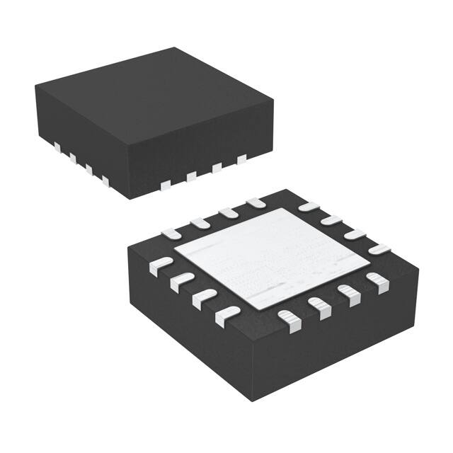
Available in 16-Pin VQFN Package
2 Applications
•
•
•
Point-of-Load Regulation From 12-V Buses
Organizers, PDAs, and Handheld PCs
Handheld Scanners
The TPS6211x devices are synchronous pulse width
modulation (PWM) converters with integrated N- and
P-channel power MOSFET switches. Synchronous
rectification is used to increase efficiency and to
reduce external component count. To achieve highest
efficiency over a wide load-current range, the
converter enters a power-saving, pulse frequency
modulation (PFM) mode at light load currents.
Operating frequency is typically 1 MHz, allowing the
use of small inductor and capacitor values. The
device can be synchronized to an external clock
signal in the range of 0.8 MHz to 1.4 MHz. For lownoise operation, the converter can be operated in
PWM-only mode. In shutdown mode, the current
consumption is reduced to less than 2 µA. The
TPS6211x family of devices are available in the 16pin (RSA) VQFN package, and operate over a freeair temperature range of –40°C to 85°C.
Device Information(1)
PART NUMBER
PACKAGE
BODY SIZE (NOM)
TPS62110
TPS62111
VQFN (16)
TPS62112
4.00 mm × 4.00 mm
TPS62113
(1) For all available packages, see the orderable addendum at
the end of the data sheet.
4 Typical Application Schematic
6.8 mH
VI = 3.8 V to 17 V
TPS62111
Efficiency vs Output Current
TPS62111
VIN
VIN
EN
SW
SW
VINA
PG
VO = 3.3 V
100
1 MW
4.2 V
1 mF
LBO
AGND
LBI
CO = 22 mF
6.3 V
80
FB
SYNC
GND GND PwPD PGND PGND
Efficiency - %
CI = 10 mF
25 V
90
5V
70
60
8.4 V
50
12 V
40
30
VO = 3.3 V
o
TA = 25 C
PFM Mode
20
10
0
0.0001
0.001
0.01
0.1
1
10
IO - Output Current- A
1
An IMPORTANT NOTICE at the end of this data sheet addresses availability, warranty, changes, use in safety-critical applications,
intellectual property matters and other important disclaimers. PRODUCTION DATA.
�TPS62110, TPS62111, TPS62112, TPS62113
SLVS585E – JULY 2005 – REVISED JUNE 2015
www.ti.com
Table of Contents
1
2
3
4
5
6
7
8
9
Features ..................................................................
Applications ...........................................................
Description .............................................................
Typical Application Schematic.............................
Revision History.....................................................
Device Comparison Table.....................................
Pin Configuration and Functions .........................
Specifications.........................................................
1
1
1
1
2
4
4
5
8.1
8.2
8.3
8.4
8.5
8.6
5
5
5
5
6
8
Absolute Maximum Ratings .....................................
ESD Ratings..............................................................
Recommended Operating Conditions.......................
Thermal Information ..................................................
Electrical Characteristics...........................................
Typical Characteristics ..............................................
Detailed Description .............................................. 9
9.1 Overview ................................................................... 9
9.2 Functional Block Diagram ....................................... 10
9.3 Feature Description................................................. 10
9.4 Device Functional Modes........................................ 12
10 Application and Implementation........................ 15
10.1 Application Information.......................................... 15
10.2 Typical Applications .............................................. 15
10.3 System Examples ................................................. 22
11 Power Supply Recommendations ..................... 23
12 Layout................................................................... 23
12.1 Layout Guidelines ................................................. 23
12.2 Layout Example .................................................... 24
13 Device and Documentation Support ................. 25
13.1
13.2
13.3
13.4
13.5
13.6
Device Support......................................................
Related Links ........................................................
Community Resources..........................................
Trademarks ...........................................................
Electrostatic Discharge Caution ............................
Glossary ................................................................
25
25
25
25
25
25
14 Mechanical, Packaging, and Orderable
Information ........................................................... 25
5 Revision History
NOTE: Page numbers for previous revisions may differ from page numbers in the current version.
Changes from Revision D (January 2014) to Revision E
•
Page
Added Pin Configuration and Functions section, ESD Ratings table, Feature Description section, Device Functional
Modes, Application and Implementation section, Power Supply Recommendations section, Layout section, Device
and Documentation Support section, and Mechanical, Packaging, and Orderable Information section .............................. 1
Changes from Revision C (October 2012) to Revision D
Page
•
Changed the FUNCTIONAL BLOCK DIAGRAM to include the SYNC pin .......................................................................... 10
•
Changed the Revision History list......................................................................................................................................... 22
Changes from Revision B (October 2012) to Revision C
Page
•
Changed ESD - HBM From: 4 kV To: 2 kV ............................................................................................................................ 5
•
Deleted ESD - MM.................................................................................................................................................................. 5
•
Changed ESD - CDM From: 1.5 kV To: 500 V....................................................................................................................... 5
•
Changed the CONSTANT-FREQUENCY MODE OF OPERATION (SYNC = HIGH) section ............................................. 13
Changes from Revision A (February 2009) to Revision B
Page
•
Changed Description text From: 2-cell Li-ion battery To: 2 to 4-cell Li-ion battery.. .............................................................. 1
•
Added text to the Terminal Functions EN pin description - Do not leave floating.................................................................. 4
•
Added ESD information to the ABSOLUTE MAXIMUM RATINGS table ............................................................................... 5
•
Changed From: Dissipation Ratings table To: Thermal Information table ............................................................................. 5
•
Added TPS62113 to the OUTPUT section of the Electrical Characteristics .......................................................................... 7
•
Changed Note A of the Functional Block Diagram............................................................................................................... 10
•
Changed the ENABLE section ............................................................................................................................................. 10
•
Changed the LOW-BATTERY DETECTOR (Standard Version) section ............................................................................. 11
2
Submit Documentation Feedback
Copyright © 2005–2015, Texas Instruments Incorporated
Product Folder Links: TPS62110 TPS62111 TPS62112 TPS62113
�TPS62110, TPS62111, TPS62112, TPS62113
www.ti.com
SLVS585E – JULY 2005 – REVISED JUNE 2015
•
Deleted the PwPD pin from Figure 4, .................................................................................................................................. 11
•
Changed the ENABLE/Low-Battery Detector (Enhanced Version) TPS62113 Only section ............................................... 11
•
Changed the POWER-GOOD COMPARATOR section ....................................................................................................... 11
•
Added the THERMAL SHUTDOWN section ........................................................................................................................ 12
•
Changed the SOFT START section ..................................................................................................................................... 12
•
Deleted "by pulling the SYNC pin LOW." - CONSTANT-FREQUENCY MODE OF OPERATION (SYNC = HIGH) ........... 13
•
Changed .............................................................................................................................................................................. 13
•
Changed PwPD to ETPad in Figure 6 to Figure 21 ............................................................................................................. 15
•
Changed the INPUT-CAPACITOR SELECTION section ..................................................................................................... 18
•
Changed Figure 19 and Figure 20 ....................................................................................................................................... 21
•
Added section: Layout Consideration................................................................................................................................... 23
Copyright © 2005–2015, Texas Instruments Incorporated
Submit Documentation Feedback
Product Folder Links: TPS62110 TPS62111 TPS62112 TPS62113
3
�TPS62110, TPS62111, TPS62112, TPS62113
SLVS585E – JULY 2005 – REVISED JUNE 2015
www.ti.com
6 Device Comparison Table
(1)
PACKAGED DEVICES
PLASTIC VQFN 16 PIN (1) (RSA)
OUTPUT VOLTAGE
LBI/LBO
FUNCTIONALITY
TPS62110
Adjustable 1.2 V to 16 V
Standard
TPS62111
Fixed 3.3 V
Standard
TPS62112
Fixed 5 V
Standard
TPS62113
Adjustable 1.2 V to 16 V
Enhanced
The RSA package is available in tape and reel. Add R suffix (TPS62110RSAR) to order quantities of 3000 parts per reel. Add T suffix
(TPS62110RSAT) to order quantities of 250 parts per reel.
7 Pin Configuration and Functions
PGND
SW
SW
PG
RSA Package
16-Pin VQFN
Top View
2
3
4
16 15 14 13
12
Exposed
Thermal
Pad
11
10
5 6 7 8
9
GND
GND
FB
AGND
VINA
1
SYNC
LBO
LBI
PGND
VIN
VIN
EN
Pin Functions
PIN
I/O
DESCRIPTION
NAME
NO.
AGND
9
I
Analog ground, connect to GND and PGND.
EN
4
I
Enable. A logic high enables the converter; logic low forces the device into shutdown mode reducing the
supply current to less than 2 µA. Do not leave floating.
FB
10
I
Feedback pin for the fixed output voltage versions. Connect to VOUT for these devices. For the
adjustable versions, an external resistive divider is connected to this pin. The internal voltage divider is
disabled for the adjustable versions.
GND
11, 12
I
Ground
LBI
7
I
Low-battery input. Do not leave floating.
LBO
6
O
Open-drain, low-battery output. This pin is pulled low if LBI is below its threshold. If not used, the pin
may be left floating or connected to GND.
PG
13
O
Power good comparator output. This is an open-drain output. A pullup resistor should be connected
between PG and VOUT. The output goes high when the output voltage is greater than 98.4% of the
nominal value. If not used, the pin may be left floating or connected to GND.
PGND
1, 16
I
Power ground. Connect all power grounds to this pin.
SW
14, 15
O
Connect the inductor to this pin. This pin is the switch pin and connected to the drain of the internal
power MOSFETS.
Input for synchronization to external clock signal. Synchronizes the converter switching frequency to an
external clock signal with CMOS level. Also controls power save mode by being tied high or low.
SYNC
5
I
SYNC = HIGH: Low-noise mode enabled, fixed-frequency PWM operation is forced
SYNC = LOW (GND): Power save mode enabled, PFM/PWM mode enabled
VIN
4
2, 3
I
Supply voltage input (power stage)
Submit Documentation Feedback
Copyright © 2005–2015, Texas Instruments Incorporated
Product Folder Links: TPS62110 TPS62111 TPS62112 TPS62113
�TPS62110, TPS62111, TPS62112, TPS62113
www.ti.com
SLVS585E – JULY 2005 – REVISED JUNE 2015
Pin Functions (continued)
PIN
NAME
NO.
I/O
DESCRIPTION
VINA
8
I
Supply voltage input (support circuits)
Exposed
Thermal Pad
–
–
Connect to AGND. Must be soldered to achieve appropriate power dissipation and mechanical
reliability.
8 Specifications
8.1 Absolute Maximum Ratings
over operating free-air temperature range (unless otherwise noted)
VCC
(1)
MIN
MAX
UNIT
–0.3
20
V
–1
20
Voltage at EN, SYNC, LBO, PG
–0.3
20
Voltage at LBI, FB
–0.3
7
Supply voltage at VIN, VINA
Voltage at SW
VI
IO
Output current at SW
TJ
Maximum junction temperature
TA
Operating free-air temperature
–40
Tstg
Storage temperature
–65
(1)
V
2400
mA
150
°C
85
°C
150
°C
Stresses beyond those listed under Absolute Maximum Ratings may cause permanent damage to the device. These are stress ratings
only and functional operation of the device at these or any other conditions beyond those indicated under Recommended Operating
Conditions is not implied. Exposure to absolute-maximum-rated conditions for extended periods may affect device reliability.
8.2 ESD Ratings
VALUE
V(ESD)
(1)
(2)
Electrostatic discharge
Human body model (HBM), per ANSI/ESDA/JEDEC JS-001 (1)
±2000
Charged-device model (CDM), per JEDEC specification JESD22C101 (2)
±500
UNIT
V
JEDEC document JEP155 states that 500-V HBM allows safe manufacturing with a standard ESD control process.
JEDEC document JEP157 states that 250-V CDM allows safe manufacturing with a standard ESD control process.
8.3 Recommended Operating Conditions
MIN
VCC
Supply voltage at VIN, VINA
NOM
MAX
3.1
17
Maximum voltage at PG, LBO, EN, SYNC
TJ
Operating junction temperature
UNIT
–40
V
17
V
125
°C
8.4 Thermal Information
TPS6211x
THERMAL METRIC (1)
RSA (VQFN)
UNIT
16 PINS
RθJA
Junction-to-ambient thermal resistance
48.2
°C/W
RθJC(top)
Junction-to-case (top) thermal resistance
45.4
°C/W
RθJB
Junction-to-board thermal resistance
16.3
°C/W
ψJT
Junction-to-top characterization parameter
0.5
°C/W
ψJB
Junction-to-board characterization parameter
16.4
°C/W
RθJC(bot)
Junction-to-case (bottom) thermal resistance
3.3
°C/W
(1)
For more information about traditional and new thermal metrics, see the Semiconductor and IC Package Thermal Metrics application
report, SPRA953.
Copyright © 2005–2015, Texas Instruments Incorporated
Submit Documentation Feedback
Product Folder Links: TPS62110 TPS62111 TPS62112 TPS62113
5
�TPS62110, TPS62111, TPS62112, TPS62113
SLVS585E – JULY 2005 – REVISED JUNE 2015
www.ti.com
8.5 Electrical Characteristics
VI = 12 V, VO = 3.3 V, IO = 600 mA, EN = VI, TA = –40°C to 85°C (unless otherwise noted)
PARAMETER
TEST CONDITIONS
MIN
TYP
MAX
UNIT
SUPPLY CURRENT
VI
Input voltage
I(Q)
3.1
Operating quiescent current
IO = 0 mA, SYNC = GND, VI = 7.2 V,
TA = 25°C (1)
IO = 0 mA, SYNC = GND, VI = 17 V
IQ(LBI)
Quiescent current with enhanced LBI
comparator version (TPS62113 only).
I(SD)
Shutdown current
17
20
(1)
23
V
µA
26
EN = VI , LBI = GND
10
µA
EN = GND
1.5
5
EN = GND, TA = 25°C, VI = 7.2 V
1.5
3
µA
ENABLE
VIH
EN high-level input voltage
VIL
EN low-level input voltage
1.3
V
0.3
EN trip-point hysteresis
170
Ilkg
EN input leakage current
EN = GND or VI, VI = 12 V
I(EN)
EN input current
0.6 V ≤ V(EN) ≤ 4 V
V(UVLO)
Undervoltage lockout threshold
Input voltage falling
0.01
V
mV
0.2
µA
10
20
µA
3
3.1
V
250
300
mV
VI ≥ 5.4 V; IO = 350 mA
165
250
VI = 3.5 V; IO = 200 mA
340
VI = 3 V; IO = 100 mA
490
2.8
Undervoltage lockout hysteresis
POWER SWITCH
RDS(ON)
P-channel MOSFET ON-resistance
Ilkg
P-channel MOSFET leakage current
VDS = 17 V
ILIMF
P-channel MOSFET current limit
VI = 7.2 V, VO = 3.3 V
RDS(ON)
Ilkg
N-channel MOSFET ON-resistance
N-channel MOSFET leakage current
mΩ
0.1
1
µA
2400
2600
mA
VI ≥ 5.4 V; IO = 350 mA
145
200
VI = 3.5 V; IO = 200 mA
170
VI = 3 V; IO = 100 mA
200
VDS = 17 V
0.1
2100
mΩ
2
µA
PG OUTPUT, LBI, LBO
V(PG)
Power good trip voltage
VO – 1.6%
Power good delay time
VOL
PG, LBO output-low voltage
IOL
PG, LBO sink current
Ilkg
PG, LBO output leakage current
VO ramping positive
50
VO ramping negative
200
V(FB) = 0.8 × VO nominal, IOL = 1 mA
LBI input trip voltage
Ilkg
LBI input leakage current
0.3
V(FB) = VO nominal, V(LBI) = VI
0.01
Input voltage falling
µA
V
V
100
nA
1.5%
VLBI,HYS Low-battery input hysteresis
6
0.25
1.256
10
V
mA
3
LBI input trip-point
accuracy
(1)
µs
1
Minimum supply voltage for valid power
good, LBI, LBO signal
VLBI
V
25
mV
Device is not switching.
Submit Documentation Feedback
Copyright © 2005–2015, Texas Instruments Incorporated
Product Folder Links: TPS62110 TPS62111 TPS62112 TPS62113
�TPS62110, TPS62111, TPS62112, TPS62113
www.ti.com
SLVS585E – JULY 2005 – REVISED JUNE 2015
Electrical Characteristics (continued)
VI = 12 V, VO = 3.3 V, IO = 600 mA, EN = VI, TA = –40°C to 85°C (unless otherwise noted)
PARAMETER
TEST CONDITIONS
MIN
TYP
MAX
UNIT
900
1000
1100
kHz
1400
kHz
OSCILLATOR
fS
Oscillator frequency
f(SYNC)
Synchronization range
VIH
SYNC high-level input voltage
VIL
SYNC low-level input voltage
Ilkg
SYNC input leakage current
CMOS-logic clock signal on SYNC pin
800
1.5
SYNC = GND or VIN
0.01
SYNC trip-point hysteresis
Ilkg
V
0.3
V
0.2
µA
170
0.6 V ≤ V(SYNC) ≤ 4 V
SYNC input leakage current
Duty cycle of external clock signal
10
mV
20
30%
90%
1.153
16
µA
OUTPUT
VO
Adjustable output voltage range
TPS62110
TPS62113
VFB
Feedback voltage
TPS62110
TPS62113
1.153
Ilkg
FB input leakage current
TPS62110
TPS62113
10
Feedback voltage tolerance
TPS62110 VI = 3.1 V to 17 V;
TPS62113 0 mA < IO < 1500 mA (2)
–2%
2%
TPS62111
VI = 3.8 V to 17 V;
0 mA < IO < 1500 mA (2)
–3%
3%
TPS62112
VI = 5.5 V to 17 V;
0 mA < IO < 1500 mA (2)
–3%
3%
Fixed output voltage tolerance
IO
(3)
Maximum output current
VI ≥ 3 V (once undervoltage lockout
voltage exceeded)
100
VI ≥ 3.5 V
500
VI ≥ 4.3 V
1200
VI ≥ 6 V
1500
Current into internal voltage divider for
fixed voltage versions
η
at 1 MHz
Minimum ton time for main switch
TSD
(2)
(3)
10%
nA
mA
µA
100%
100
Shutdown temperature
Start-up time
100
92%
VI = 12 V, Vo = 5 V, Io = 600 mA
Duty-cycle range for main switches
V
5
VI = 7.2 V; VO = 3.3 V; IO = 600 mA
Efficiency
V
IO = 800 mA, VI = 12 V, Vo = 3.3 V
ns
145
°C
1
ms
The maximum output current depends on the input voltage. See the maximum output current for further restrictions on the minimum
input voltage.
The output voltage accuracy includes line and load regulation over the full temperature range TA = –40°C to 85°C. See No-Load
Operation.
Copyright © 2005–2015, Texas Instruments Incorporated
Submit Documentation Feedback
Product Folder Links: TPS62110 TPS62111 TPS62112 TPS62113
7
�TPS62110, TPS62111, TPS62112, TPS62113
SLVS585E – JULY 2005 – REVISED JUNE 2015
www.ti.com
2000
1900
1800
1700
1600
1500
1400
1300
1200
1100
1000
900
800
700
600
500
400
300
200
100
0
1000
VO = 12 V
IO = 100 mA
990
o
85 C
980
Switching Frequency - kHz
IO - Output Current - mA
8.6 Typical Characteristics
o
970
25 C
960
o
-40 C
950
940
930
920
910
900
3.2
3.6
4
4.4
4.8
5.2
5.6
3
6
4
5
6
VI - Input Voltage- V
7 8 9 10 11 12 13 14 15 16 17
VI - Input Voltage - V
Figure 2. Switching Frequency vs Input Voltage
Figure 1. TPS62111 Maximum Output Current vs Input
Voltage
50
45
Quiescent Current - mA
40
35
30
o
85 C
o
25 C
25
20
o
-40 C
15
10
5
0
3
4
5
6
7 8 9 10 11 12 13 14 15 16 17
VI - Input Voltage - V
Figure 3. Quiescent Current vs Input Voltage
8
Submit Documentation Feedback
Copyright © 2005–2015, Texas Instruments Incorporated
Product Folder Links: TPS62110 TPS62111 TPS62112 TPS62113
�TPS62110, TPS62111, TPS62112, TPS62113
www.ti.com
SLVS585E – JULY 2005 – REVISED JUNE 2015
9 Detailed Description
9.1 Overview
The TPS6211x family of devices are synchronous step-down converters that operate with a 1-MHz fixedfrequency pulse-width modulation (PWM) at moderate-to-heavy load currents, and enters the power-save mode
at light load current.
During PWM operation, the converter uses a unique fast-response voltage-mode control scheme with inputvoltage feedforward. Good line and load regulation is achieved with the use of small input and output ceramic
capacitors. At the beginning of each clock cycle initiated by the clock signal (S), the P-channel MOSFET switch
is turned on, and the inductor current ramps up until the comparator trips and the control logic turns the switch
off. The switch is turned off by the current limit comparator if the current limit of the P-channel switch is
exceeded. After the dead time prevents current shoot through, the N-channel MOSFET rectifier is turned on, and
the inductor current ramps down. The next cycle is initiated by the clock signal turning off the N-channel rectifier,
and turning on the P-channel switch.
The error amplifier as well as the input voltage determines the rise time of the sawtooth generator. Therefore,
any change in input voltage or output voltage directly controls the duty cycle of the converter, giving a very good
line- and load-transient regulation.
Copyright © 2005–2015, Texas Instruments Incorporated
Submit Documentation Feedback
Product Folder Links: TPS62110 TPS62111 TPS62112 TPS62113
9
�TPS62110, TPS62111, TPS62112, TPS62113
SLVS585E – JULY 2005 – REVISED JUNE 2015
www.ti.com
9.2 Functional Block Diagram
SYNC
VIN
Current Limit Comparator
+
_
Undervoltage
Lockout
Bias Supply
VINA
REF
Thermal
Shutdown
+
_
Soft Start
V
V(COMP)
I
IAVG Comparator
REF
1-MHz
Oscillator
P-Channel
Power MOSFET
Sawtooth
Generator
Comparator
S
+
_
R
Driver
Shoot-Through
Logic
Control
Logic
SW
N-Channel
Power MOSFET
Comparator High
Comparator Low
Comparator High 2
Load Comparator
+
_
SKIP Comparator
+
_
PG
+
_
Comparator High
+
Gm
_
Comparator Low
+
R2
VREF = 1.153 V
EN
+
_
LBO
_
R1
Compensation
+
_
(See Note A)
FB
1.256 V
LBI
PGND
GND
For the adjustable version (TPS62110 and TPS62113), the internal feedback divider is disabled and the FB pin is
directly connected to the internal compensation block.
9.3 Feature Description
9.3.1 Enable
A logic low on EN forces the TPS6211x devices into shutdown. In shutdown, the power switch, drivers, voltage
reference, oscillator, and all other functions are turned off. The LBO pin is high impedance, while PG is held low.
The supply current is reduced to less than 2 µA in the shutdown mode. When the device is in thermal shutdown,
the band gap is forced to be switched on even if the device is set into shutdown by pulling EN to GND.
10
Submit Documentation Feedback
Copyright © 2005–2015, Texas Instruments Incorporated
Product Folder Links: TPS62110 TPS62111 TPS62112 TPS62113
�TPS62110, TPS62111, TPS62112, TPS62113
www.ti.com
SLVS585E – JULY 2005 – REVISED JUNE 2015
Feature Description (continued)
If an output voltage is present when the device is disabled, which could be due to an external voltage source or a
super capacitor, the reverse leakage current is specified under electrical characteristics. Pulling the enable pin
high starts up the TPS6211x devices with the soft-start. If the EN pin is connected to any voltage other than VI or
GND, an increased leakage current of typically 10 µA and up to 20 µA can occur. See TPS6211x Driving EN and
SYNC Pins (SLVA295) for details.
9.3.2 Low-Battery Detector (Standard Version)
The low-battery output (LBO) is an open-drain type which goes low when the voltage at the low-battery input
(LBI) falls below the trip point of 1.256 V ±1.5%. The voltage at which the low-battery warning is issued can be
adjusted with a resistive divider as shown in Figure 4. TI recommends the sum of resistors R1 + R2 as well as
the sum of resistors R5 + R6 to be in the 100-kΩ to 1-MΩ range for high efficiency at low output current. An
external pullup resistor can be connected to VO, or any other voltage rail in the voltage range of 0 V to 17 V.
During start-up, the LBO output signal is invalid for the first 500 µs. LBO is high-impedance when the device is
disabled. If the low-battery comparator function is not used, connect LBI to ground. The low-battery detector is
disabled when the device is disabled.
When the LBI is used to supervise the battery voltage and shut down the TPS6211x devices at low-input
voltages, the battery voltage rises when its current drops to zero. The implemented hysteresis on the LBI pin
may not be sufficient for all types of batteries. Figure 4 shows how an additional external hysteresis can be
implemented. See Adding Hysteresis to Low-Battery Input on the TPS62113 (SLVA373) for details.
6.8 mH
VI = 4.3 V to 17 V
2
3
4
TPS62110
VIN
VIN
EN
SW
SW
15
R3
R5
8
CI = 10 mF
25 V
PG
VINA
1 mF
9
7
5
R6
AGND
6
FB
10
SYNC
GND GND
12
R4
Cff
10 pF
R1
560 kW
13
LBO
LBI
11
VO = 3.3 V
14
CO = 22 mF
6.3 V
R7
R2
300 kW
PGND PGND
1
16
Figure 4. LBI With Increased Hysteresis
9.3.3 Enable/Low-Battery Detector - Enhanced Version (TPS62113 Only)
The TPS62113 device offers an enhanced LBI functionality to provide a precise, user-programmable
undervoltage shutdown. No additional supply voltage supervisor (SVS) is needed to provide this function. When
the enable (EN) pin is pulled high, only the internal bandgap voltage reference is switched on to provide a
reference source for the LBI comparator. As long as the voltage at LBI is less than the LBI trip point, all other
internal circuits are shut down, reducing the supply current to 10 µA. As soon as input voltage at LBI rises above
the LBI trip point of 1.256 V, the device is completely enabled and starts switching.
This functionality is the only difference between the TPS62110 and TPS62113 devices.
9.3.4 Power Good Comparator
The power good (PG) comparator is an open-drain output capable of sinking 1 mA (typical). The PG is only
active when the device is enabled (EN = high). When the device is disabled (EN = low), the PG pin is pulled to
GND.
The PG output is only valid after a 250-µs delay when the device is enabled and the supply voltage is greater
than the undervoltage lockout V(UVLO).
The PG pin becomes active-high when the output voltage exceeds 98.4% (typical) of its nominal value. Leave
the PG pin floating or grounded when not used.
Copyright © 2005–2015, Texas Instruments Incorporated
Submit Documentation Feedback
Product Folder Links: TPS62110 TPS62111 TPS62112 TPS62113
11
�TPS62110, TPS62111, TPS62112, TPS62113
SLVS585E – JULY 2005 – REVISED JUNE 2015
www.ti.com
Feature Description (continued)
9.3.5 Undervoltage Lockout
The undervoltage lockout (UVLO) circuit prevents the device from misoperation at low-input voltages. It prevents
the converter from turning on the switch or rectifier MOSFET under undefined conditions. The minimum input
voltage to start up the TPS6211x devices is 3.4 V (worst case). The device shuts down at 2.8 V minimum.
9.3.6 Synchronization
If no clock signal is applied, the converter operates with a typical switching frequency of 1 MHz. It is possible to
synchronize the converter to an external clock within a frequency range from 0.8 MHz to 1.4 MHz only. The
device automatically detects the rising edge of the first clock and synchronizes immediately to the external clock.
If the clock signal is stopped, the converter automatically switches back to the internal clock and continues
operation. The switch over is initiated if no rising edge on the SYNC pin is detected for a duration of four clock
cycles. Therefore, the maximum delay time can be 6.25 µs if the internal clock has its minimum frequency of 800
kHz.
If the device is synchronized to an external clock, the power save mode is disabled, and the devices stay in
forced PWM mode.
Connecting the SYNC pin to the GND pin enables the power save mode. The converter operates in the PWM
mode at moderate-to-heavy loads, and in the PFM mode during light loads, which maintains high efficiency over
a wide load current range.
9.3.7 Thermal Shutdown
The junction temperature (TJ) of the device is monitored by an internal temperature sensor. If TJ exceeds 145°C
typical, the device goes into thermal shutdown. Both the high-side and low-side power FETs are turned off and
PG goes high impedance. When TJ decreases by typically 10°C, the converter resumes normal operation.
9.4 Device Functional Modes
9.4.1 Soft Start
The TPS6211x has an internal soft-start circuit that limits the inrush current during start-up. This prevents
possible voltage drops of the input voltage when a battery or a high-impedance power source is connected to the
input of the TPS6211x devices.
The soft start is implemented as a digital circuit increasing the switch current in steps of 300 mA, 600 mA, and
1200 mA for 250 µs each. Then, the switch current limit is set to 2.4 A typical. Therefore, the start-up time
depends on the output capacitor and load current. Typical start-up time with a 22-µF output capacitor and 800mA load current is 1 ms.
The TPS6211x devices can start into a prebiased output. During monotonic prebiased start-up, the N-channel
MOSFET is not allowed to turn on until the internal ramp of the device sets an output voltage greater than the
prebias voltage.
9.4.2 Constant-Frequency Mode of Operation (Sync = High)
In constant-frequency mode, the output voltage is regulated by varying the duty cycle of the PWM signal in the
range of 100% to 10%. Connecting the SYNC pin to a voltage greater than 1.5 V forces the converter to operate
permanently in the PWM mode even at light- or no-load currents. The advantage is that the converter operates
with a fixed switching frequency that allows simple filtering of the switching frequency for noise-sensitive
applications. In this mode, the efficiency is lower compared to the power-save mode during light loads. The NMOSFET of the devices stays on even when the current into the output drops to zero. This prevents the device
from going into discontinuous mode, and the device transfers unused energy back to the input. Therefore, there
is no ringing at the output, which usually occurs in discontinuous mode. The duty cycle range in constantfrequency mode is 100% to 10%.
12
Submit Documentation Feedback
Copyright © 2005–2015, Texas Instruments Incorporated
Product Folder Links: TPS62110 TPS62111 TPS62112 TPS62113
�TPS62110, TPS62111, TPS62112, TPS62113
www.ti.com
SLVS585E – JULY 2005 – REVISED JUNE 2015
Device Functional Modes (continued)
9.4.3 Power Save Mode of Operation (Sync = Low)
As the load current decreases, the converter enters the power-save mode of operation. During power-save
mode, the converter operates with reduced switching frequency in pulse-frequency modulation (PFM), and with a
minimum quiescent current to maintain high efficiency. Whenever the average output current goes below the skip
threshold, the converter enters the power-save mode. The average current depends on the input voltage. It is
about 200 mA at low input voltages and up to 400 mA with maximum input voltage. The average output current
must be less than the threshold for at least 32 clock cycles to enter the power-save mode. During the powersave mode, the output voltage is monitored with a comparator, and the output voltage is regulated to a typical
value between the nominal output voltage and 0.8% above the nominal output voltage. When the output voltage
falls below the nominal output voltage, the P-channel switch turns on. The P-channel switch is turned off as the
peak switch current is reached. The N-channel rectifier is turned on, and the inductor current ramps down. As the
inductor current approaches zero, the N-channel rectifier is turned off and the switch is turned on starting the
next pulse. When the output voltage cannot be reached with a single pulse, the device continues to switch with
its normal operating frequency until the comparator detects the output voltage to be 0.8% above the nominal
output voltage. This control method reduces the quiescent current to 20 µA (typical), and reduces the switching
frequency to a minimum that achieves the highest converter efficiency. Figure 5 shows the typical power save
mode operation.
1.6%
0.8%
VO (nominal)
–1.6%
t
Figure 5. Power Save Mode Output-Voltage Thresholds
Use Equation 1 the typical PFM (SKIP) current threshold for the TPS6211x devices.
VI
ISKIP »
25 W
(1)
Equation 1 is valid for input voltages up to 7 V. For higher voltages, the skip current threshold is not increased
further. The converter enters the fixed-frequency PWM mode as soon as the output voltage falls below VO –
1.6% (nominal).
9.4.4 100% Duty-Cycle, Low-Dropout Operation
The TPS6211x devices offer the lowest possible input-to-output voltage difference while still maintaining
operation with the use of the 100% duty-cycle mode. In this mode, the P-channel switch is constantly turned on.
This is particularly useful in battery-powered applications to achieve the longest operation time, taking full
advantage of the whole battery voltage range. The minimum input voltage to maintain regulation depends on the
load current and output voltage, and is calculated using Equation 2.
VI(min) = VO(max) + IO(max) ´ (RDS(ON)(max) + RL )
IO (max) = Maximum output current plus inductor ripple current
RDS(ON)(max) = Maximum P-Channel switch resistance
RL = DC resistance of the inductor
VO(max) = Nominal output voltage plus maximum output voltage tolerance
Copyright © 2005–2015, Texas Instruments Incorporated
Submit Documentation Feedback
Product Folder Links: TPS62110 TPS62111 TPS62112 TPS62113
(2)
13
�TPS62110, TPS62111, TPS62112, TPS62113
SLVS585E – JULY 2005 – REVISED JUNE 2015
www.ti.com
Device Functional Modes (continued)
9.4.5 No-Load Operation
When the converter operates in the forced PWM mode and there is no load connected to the output, the
converter regulates the output voltage by allowing the inductor current to reverse for a short time.
14
Submit Documentation Feedback
Copyright © 2005–2015, Texas Instruments Incorporated
Product Folder Links: TPS62110 TPS62111 TPS62112 TPS62113
�TPS62110, TPS62111, TPS62112, TPS62113
www.ti.com
SLVS585E – JULY 2005 – REVISED JUNE 2015
10 Application and Implementation
NOTE
Information in the following applications sections is not part of the TI component
specification, and TI does not warrant its accuracy or completeness. TI’s customers are
responsible for determining suitability of components for their purposes. Customers should
validate and test their design implementation to confirm system functionality.
10.1 Application Information
The TPS6211x devices are a family of low-noise synchronous step-down DC-DC converters that are ideally
suited for systems powered from a 2- to 4-cell Li-ion battery or from a 12-V or 15-V rail.
10.2 Typical Applications
10.2.1 Standard Connection for Adjustable Version
TDK 6.8 mH
SLF7032T-6R8M1R6
Vbat
R5
VIN
VIN
EN
open
C1
CI 10 mF / 25 V
TDK
C3225X5R1E106K
TPS62110
VINA
1 mF
AGND
LBI
SW
SW
VO
L1
R3
1 MW
R4
1 MW
R1
Cff
PG
CO 22 mF / 16 V
TDK
C3225X7R1C226M
LBO
FB
R2
R6
261 kW
SYNC
VIN or
GND
GND GND
Pad PGND PGND
For an output voltage lower than 2.5 V, TI recommends an output capacitor of 33 μF or greater to improve load
transient performance.
Figure 6. Standard Connection for Adjustable Version
10.2.1.1 Design Requirements
The design guidelines provide a component selection to operate the device within the Recommended Operating
Conditions.
Table 1. Bill of Materials for the Adjustable Version
REFERENCE
PART NUMBER
VALUE
MANUFACTURER
Ci
C3225X5R1E106K
10 µF
TDK
Co
C3225X7R1C226M
22 µF
TDK
L1
SLF7032T-6R8M1R6
6.8 µH
TDK
C1
TMK212B7105KG-T
1 µF
Taiyo Yuden
IC1
TPS62110
-
Texas Instruments
R1
generic metal film resistor; tolerance
1%
220 kΩ (depending on desired output
voltage)
—
R2
generic metal film resistor; tolerance
1%
390 kΩ (depending on desired output
voltage)
—
R3, R4
generic metal film resistor; tolerance
1%
1 MΩ
—
R5
generic metal film resistor; tolerance
1%
open
—
R6
generic metal film resistor; tolerance
1%
261 kΩ
—
Copyright © 2005–2015, Texas Instruments Incorporated
Submit Documentation Feedback
Product Folder Links: TPS62110 TPS62111 TPS62112 TPS62113
15
�TPS62110, TPS62111, TPS62112, TPS62113
SLVS585E – JULY 2005 – REVISED JUNE 2015
www.ti.com
Typical Applications (continued)
Table 1. Bill of Materials for the Adjustable Version (continued)
REFERENCE
PART NUMBER
VALUE
MANUFACTURER
C(ff)
generic ceramic capacitor; COG
10 pF (depending on output voltage)
—
10.2.1.2 Detailed Design Procedure
The graphs were generated using the EVM with the setup according to Figure 6, unless otherwise noted. Graphs
for an output voltage of 1.5 V and 1.8 V were generated using the TPS62110 device with the output voltage
dividers adjusted according Table 2.
VO = VFB ´
æ V ö
R1 = R2 ´ ç O ÷ - R2
è VFB ø
R1 + R2
R2
VFB = 1.153 V
(3)
Table 2. Recommended Resistors
OUTPUT VOLTAGE
R1
R2
NOMINAL VOLTAGE
TYPICAL Cff
9V
680 kΩ
100 kΩ
8.993 V
22 pF
5V
510 kΩ
150 kΩ
5.073 V
10 pF
3.3 V
560 kΩ
300 kΩ
3.305 V
10 pF
2.5 V
390 kΩ
330 kΩ
2.515 V
10 pF
1.8 V
220 kΩ
390 kΩ
1.803 V
10 pF
1.5 V
100 kΩ
330 kΩ
1.502 V
10 pF
10.2.1.2.1 External Component Selection
The control loop of the TPS6211x family of devices requires a certain value for the output inductor and the output
capacitor for stable operation. As long as the nominal value of L × C ≥ 6.2 µH × 22 µF, the control loop has
enough phase margin and the device is stable. Reducing the inductor value without increasing the output
capacitor (or vice versa) may cause stability problems. There are applications where it may be useful to increase
the value of the output capacitor, and so on, for a low-transient output-voltage change. From a stability point of
view, the inductor value could be decreased to keep the L × C product constant. However, there are drawbacks if
the inductor value is decreased. A low inductor value causes a high inductor ripple current, and therefore
reduces the maximum DC output current. Table 3 gives the advantages and disadvantages when designing the
inductor and output capacitor.
Table 3. Advantages and Disadvantages When Designing the Inductor and Output Capacitor
INFLUENCE ON STABILITY
ADVANTAGE
DISADVANTAGE
Less output voltage ripple
Increase Cout (>22 µF)
Uncritical
Decrease Cout (6.8 µH
also
Less output voltage overshoot /
undershoot during load transient
None
Higher-output voltage ripple
High-output voltage overshoot /
undershoot during load
transient
None
Less gain and phase margin
Increase L (>6.8 µH)
16
Less inductor current ripple
More energy stored in the
inductor → higher voltage
overshoot during load transient
Higher DC output current possible if
operated close to the current limit
Smaller current rise → higher
voltage undershoot during load
transient → do not decrease the
value of Cout due to these
effects
Uncritical
Submit Documentation Feedback
Copyright © 2005–2015, Texas Instruments Incorporated
Product Folder Links: TPS62110 TPS62111 TPS62112 TPS62113
�TPS62110, TPS62111, TPS62112, TPS62113
www.ti.com
SLVS585E – JULY 2005 – REVISED JUNE 2015
Table 3. Advantages and Disadvantages When Designing the Inductor and Output Capacitor (continued)
INFLUENCE ON STABILITY
Critical
Decrease L (
22 µF also
ADVANTAGE
DISADVANTAGE
Small voltage overshoot and undershoot
during load transient
High inductor current ripple
especially at high input voltage
and low output voltage
10.2.1.2.2 Inductor Selection
As shown in Table 3, the inductor value can be increased to greater values. For good performance, the peak-topeak inductor-current ripple should be less than 30% of the maximum DC output current. Especially at input
voltages greater than 12 V, it makes sense to increase the inductor value to keep the inductor-current ripple low.
In such applications, the inductor value can be increased to 10 µH or 22 µH. Values greater than 22 µH should
be avoided to keep the voltage overshoot during load transient in an acceptable range.
After choosing the inductor value, two additional inductor parameters should be considered:
• Current rating of the inductor
• DC resistance
The DC resistance of the inductance directly influences the efficiency of the converter. Therefore, an inductor
with lowest DC resistance should be selected for highest efficiency. To avoid saturation of the inductor, the
inductor should be rated at least for the maximum output current plus the inductor ripple current which is
calculated using Equation 4.
V
1- O
VI
DI
IL max = IO max + L
DIL = VO ´
L´f
2
where
•
•
•
•
f = Switching frequency (1000 kHz typical)
L = Inductor value
ΔIL = Peak-to-peak inductor ripple current
IL(max) = Maximum inductor current
(4)
The highest inductor current occurs at maximum VI. A more conservative approach is to select the inductor
current rating just for the maximum switch current of the TPS6211x, which is 2.4 A (typically). See Table 4 for
recommended inductors.
Table 4. List of Inductors
MANUFACTURER
Coilcraft
PART NO.
INDUCTANCE
DC RESISTANCE
SATURATION CURRENT
MSS6132-682
6.8 µH
65 mΩ (maximum)
1.5 A
HA3808-AL
6.8 µH
99 mΩ (typical)
4.4 A
Epcos
B82462G4682M
6.8 µH
50 mΩ (maximum)
1.5 A
Sumida
CDRH5D28-6R2
6.2 µH
33 mΩ (typical)
1.8 A
SLF6028T-6R8M1R5
6.8 µH
35 mΩ (typical)
1.5 A
SLF7032T-6R8M1R6
6.8 µH
41 mΩ (typical)
1.6 A
7447789006
6.8 µH
44 mΩ (typical)
2.75 A
7447779006
6.8 µH
33 mΩ (typical)
3.3 A
744053006
6.2 µH
45 mΩ (typical)
1.8 A
TDK
Wurth
10.2.1.2.3 Output Capacitor Selection
A 22-μF (typical) output capacitor is needed with a 6.8-μH inductor. For an output voltage greater than 5 V, a 33μF (minimum) output capacitor is required for stability. For best performance, a low-ESR ceramic output
capacitor is needed.
The RMS ripple current is calculated using Equation 5.
Copyright © 2005–2015, Texas Instruments Incorporated
Submit Documentation Feedback
Product Folder Links: TPS62110 TPS62111 TPS62112 TPS62113
17
�TPS62110, TPS62111, TPS62112, TPS62113
SLVS585E – JULY 2005 – REVISED JUNE 2015
www.ti.com
VO
VI
1
IRMS (CO ) = VO ´
´
L´f
2´ 3
1-
(5)
The overall output ripple voltage is the sum of the voltage spike caused by the output capacitor ESR plus the
voltage ripple caused by charging and discharging the output capacitor:
V
1- O
ö
VI æ
1
DVO = VO ´
´ç
+ RESR ÷
L´f
è 8 ´ CO ´ f
ø
where
•
the highest output voltage ripple occurs at the highest input voltage VI.
(6)
10.2.1.2.4 Input Capacitor Selection
The nature of the buck converter is a pulsating input current; therefore, a low ESR input capacitor is required for
best input voltage filtering and for minimizing the interference with other circuits caused by high input voltage
spikes. The input capacitor should have a minimum value of 10 µF and can be increased without any limit for
better input voltage filtering. The input capacitor should be rated for the maximum input ripple current and is
calculated using Equation 7.
IRMS = IO max ´
VO æ
V ö
´ ç1 - O ÷
VI è
VI ø
(7)
The worst-case RMS ripple current occurs at D = 0.5 and is calculated as: IRMS = IO/2. Ceramic capacitors show
a good performance because of their low ESR value, and they are less sensitive against voltage transients
compared to tantalum capacitors. Place the input capacitor as close as possible to the VIN and PGND pins of the
IC for best performance.
An additional 1-µF input capacitor is required from VINA to AGND. VIN and VINA must be connected to the
same source. TI does not recommend an RC filter from VIN to VINA.
10.2.1.2.5 Feedforward Capacitor Selection
The feedforward capacitor (Cff) is needed to compensate for parasitic capacitance from the feedback pin to GND.
Typically, a value of 4.7 pF to 22 pF is needed for an output voltage divider with a equivalent resistance (R1 in
parallel with R2) in the 150-kΩ range. The value can be chosen based on best transient performance and lowest
output voltage ripple in PFM mode.
10.2.1.2.6 Recommended Capacitors
TI recommends using only X5R or X7R ceramic capacitors as input and output capacitors. Ceramic capacitors
show a DC-bias effect. This effect reduces the effective capacitance when a DC-bias voltage is applied across a
ceramic capacitor, as on the output and input capacitor of a DC-DC converter. The effect may lead to a
significant capacitance drop, especially for high input and output voltages and small capacitor packages. See the
manufacturer's data sheet about the performance with a DC bias voltage applied. It may be necessary to choose
a higher voltage rating or nominal capacitance value to get the required value at the operating point. The
capacitors listed in Table 5 have been tested with the TPS6211x devices with good performance.
Table 5. List of Capacitors
MANUFACTURER
Taiyo Yuden
PART NUMBER
SIZE
VOLTAGE
CAPACITANCE
TMK316BJ106KL
1206
25 V
10 µF
EMK325BJ226KM
1210
16 V
22 µF
25 V
10 µF
16 V
22 µF
25 V
10 µF
C3225X5R1E106M
TDK
C3225X7R1C226M
C3216X5R1E106MT
18
Submit Documentation Feedback
1210
1206
TYPE
Ceramic
Ceramic
Copyright © 2005–2015, Texas Instruments Incorporated
Product Folder Links: TPS62110 TPS62111 TPS62112 TPS62113
�TPS62110, TPS62111, TPS62112, TPS62113
www.ti.com
SLVS585E – JULY 2005 – REVISED JUNE 2015
10.2.1.3 Application Curves
100
100
90
90
80
80
4.2 V
5V
60
Efficiency - %
Efficiency - %
4.2 V
70
8.4 V
5V
50
12 V
40
30
70
8.4 V
60
50
40
12 V
30
VO = 1.8 V
o
TA = 25 C
PWM Mode
20
10
0
0.0001
0.001
0.01
0.1
10
0
0.0001
10
1
VO = 1.8 V
o
TA = 25 C
PFM Mode
20
0.001
0.1
1
10
Figure 8. TPS62110 Efficiency vs Output Current
Figure 7. TPS62110 Efficiency vs Output Current
100
100
90
90
4.2 V
80
70
5V
60
4.2 V
80
Efficiency - %
Efficiency - %
0.01
IO - Output Current- A
IO - Output Current- A
8.4 V
50
40
12 V
30
70
5V
60
8.4 V
50
40
12 V
30
VO = 1.5 V
o
TA = 25 C
PWM Mode
20
10
0
0.0001
0.001
0.01
0.1
10
0
0.0001
10
1
VO = 1.5 V
o
TA = 25 C
PFM Mode
20
0.001
0.01
0.1
1
10
IO - Output Current- A
IO - Output Current- A
Figure 10. TPS62110 Efficiency vs Output Current
Figure 9. TPS62110 Efficiency vs Output Current
10.2.2 Standard Connection for Fixed-Voltage Version
6.8 mH
VI = 5.5 V to 17 V
2
3
4
8
CI = 10 mF
25 V
C1
1 mF
9
7
5
TPS62112
15
VIN
VIN
EN
SW
SW
VINA
PG
14
VO = 5 V
L1
R3
1 MW
13
LBO
6
FB
10
CO = 22 mF
10 V
AGND
LBI
SYNC
GND GND
11
12
ET
Pad PGND PGND
1
16
Figure 11. Standard Connection for Fixed-Voltage Version
10.2.2.1 Design Requirements
The design guidelines provide a component selection to operate the device within the Recommended Operating
Conditions.
Copyright © 2005–2015, Texas Instruments Incorporated
Submit Documentation Feedback
Product Folder Links: TPS62110 TPS62111 TPS62112 TPS62113
19
�TPS62110, TPS62111, TPS62112, TPS62113
SLVS585E – JULY 2005 – REVISED JUNE 2015
www.ti.com
Table 6. Bill of Materials for the Fixed Voltage Versions
REFERENCE
PART NUMBER
VALUE
MANUFACTURER
Ci
C3225X5R1E106K
10 µF
TDK
TDK
Co
C3225X7R1C226M
22 µF
L1
SLF7032T-6R8M1R6
6.8 µH
TDK
C1
TMK212B7105KG-T
1 µF
Taiyo Yuden
IC1
TPS62112
—
Texas Instruments
R3
generic metal film resistor; tolerance
1%
1 MΩ
—
10.2.2.2 Detailed Design Procedure
The graphs were generated using the EVM with the setup according to Figure 6, unless otherwise noted. Graphs
for an output voltage of 5 V and 3.3 V were generated using the TPS62111 and TPS62112 devices with R1 = 0
Ω and R2 = open.
10.2.2.3 Application Curves
100
100
90
90
80
80
8.4 V
Efficiency - %
Efficiency - %
8.4 V
70
60
12 V
50
15 V
40
30
12 V
60
50
15 V
40
30
VO = 5 V
o
TA = 25 C
PWM Mode
20
10
0
0.0001
70
0.001
0.01
0.1
1
20
10
VO = 5 V
o
TA = 25 C
PFM Mode
0
0.0001
10
0.001
IO - Output Current- A
0.01
0.1
1
10
IO - Output Current- A
Figure 12. TPS62112 Efficiency vs Output Current
Figure 13. TPS62112 Efficiency vs Output Current
100
100
90
90
4.2 V
80
80
Efficiency - %
Efficiency - %
4.2 V
70
8.4 V
60
5V
50
12 V
40
30
10
8.4 V
50
12 V
40
0.001
0.01
0.1
1
10
10
Figure 14. TPS62111 Efficiency vs Output Current
Submit Documentation Feedback
VO = 3.3 V
o
TA = 25 C
PFM Mode
20
IO - Output Current- A
20
60
30
VO = 3.3 V
o
TA = 25 C
PWM Mode
20
0
0.0001
5V
70
0
0.0001
0.001
0.01
0.1
1
10
IO - Output Current- A
Figure 15. TPS62111 Efficiency vs Output Current
Copyright © 2005–2015, Texas Instruments Incorporated
Product Folder Links: TPS62110 TPS62111 TPS62112 TPS62113
�TPS62110, TPS62111, TPS62112, TPS62113
www.ti.com
SLVS585E – JULY 2005 – REVISED JUNE 2015
100
90
Efficiency - %
80
VO = 3.3 V
SYNC = 1.4 MHz
o
TA = 25 C
PWM Mode
VI = 5 V/div
70
8.4 V
60
5V
50
12 V
VO = 50 mV/div
40
30
VI = 7.2 V to 12 V
VO = 3.3 V
ILOAD = 800 mA
o
TA = 25 C
20
10
0
0.0001
t - Time = 2 ms/div
0.001
0.01
0.1
10
1
IO - Output Current- A
Figure 17. TPS62111 Line Transient
Figure 16. TPS62111 Efficiency vs Output Current
VI = 8.4 V, VO = 3.3 V
VI = 8.4 V
VO = 3.3 V
ILOAD = 150 mA to 1350 mA
TA = 25°C
o
ILOAD = 100 mA, TA = 25 C
VO = 20 mV/div
SW =
5 V/div
VO = 50 mV/div
IO = 500 mA/div
t - Time = 20 µs/div
ICOIL = 200 mA/div
t - Time = 5 ms/div
Figure 19. TPS62111 Output Ripple
Figure 18. TPS62111 Load Transient
VI = 12 V, VO = 3.3 V
o
ILOAD = 800 mA, TA = 25 C
EN = 10 V/div
VO = 1 V/div
ICOIL = 500 mA/div
SW = 5 V/div
t - Time = 200 ms/div
Figure 20. TPS62111 Start-up Timing
Copyright © 2005–2015, Texas Instruments Incorporated
Submit Documentation Feedback
Product Folder Links: TPS62110 TPS62111 TPS62112 TPS62113
21
�TPS62110, TPS62111, TPS62112, TPS62113
SLVS585E – JULY 2005 – REVISED JUNE 2015
www.ti.com
10.3 System Examples
The TPS62110 device can be used within an adjustable output voltage range from 1.2 V to 16 V. Figure 21
shows and application example with 9-V output.
6.8 mH
VI = 9.3 V to 17 V
2
3
4
8
CI = 10 mF
25 V
TPS62110
VIN
VIN
EN
9
5
15
VO = 9 V
14
1 MW
PG
VINA
1 mF
7
AGND
13
LBO
6
FB
10
LBI
Cff
11
12
22 pF
R1
680 kW
CO = 33 mF
16 V
(See Note A)
R2
100 kW
SYNC
GND GND
A.
SW
SW
ET
Pad PGND PGND
1
16
For an output voltage greater than 5 V, an output capacitor of 33 μF minimum is required for stability.
Figure 21. Application With 9-V Output
22
Submit Documentation Feedback
Copyright © 2005–2015, Texas Instruments Incorporated
Product Folder Links: TPS62110 TPS62111 TPS62112 TPS62113
�TPS62110, TPS62111, TPS62112, TPS62113
www.ti.com
SLVS585E – JULY 2005 – REVISED JUNE 2015
11 Power Supply Recommendations
The TPS6211x family of devices has no special requirements for its input power supply. The output current of the
input power supply must be rated according to the supply voltage, output voltage, and output current of the
TPS6211x devices.
12 Layout
12.1 Layout Guidelines
A proper layout is critical for the operation of a switched-mode power supply (SMPS), even more at high
switching frequencies. Therefore, the PCB layout of the TPS6211x devices demands careful attention to ensure
operation and to get the performance specified. A poor layout can lead to issues like poor regulation (both line
and load), stability and accuracy weaknesses, increased EMI radiation, and noise sensitivity.
Provide low inductive and resistive paths for loops with high di/dt. Therefore, paths conducting the switched load
current should be as short and wide as possible. The input and output capacitance should be placed as close as
possible to the IC pins and parallel wiring over long distances as well as narrow traces should be avoided.
Provide low capacitive paths (with respect to all other nodes) for wires with high dv/dt. Therefore, keep the SW
node small. Loops which conduct an alternating current should outline an area as small as possible, as this area
is proportional to the energy radiated.
Sensitive nodes like FB and LBI need to be connected with short wires and not nearby high dv/dt signals (that is,
SW). The FB resistors, R1 and R2, and LBI resistors, R5 and R6, should be kept close to the IC and connect
directly to those pins and AGND. The 1-µF capacitor on VINA should connect directly from VINA to AGND.
All grounds (GND, AGND, and PGND) are directly connected to the exposed thermal pad. The exposed thermal
pad must be soldered to the circuit board for mechanical reliability and to achieve appropriate power dissipation.
See Figure 22 for the recommended layout of the TPS6211x.
Copyright © 2005–2015, Texas Instruments Incorporated
Submit Documentation Feedback
Product Folder Links: TPS62110 TPS62111 TPS62112 TPS62113
23
�TPS62110, TPS62111, TPS62112, TPS62113
SLVS585E – JULY 2005 – REVISED JUNE 2015
www.ti.com
12.2 Layout Example
Figure 22. Recommended Layout
24
Submit Documentation Feedback
Copyright © 2005–2015, Texas Instruments Incorporated
Product Folder Links: TPS62110 TPS62111 TPS62112 TPS62113
�TPS62110, TPS62111, TPS62112, TPS62113
www.ti.com
SLVS585E – JULY 2005 – REVISED JUNE 2015
13 Device and Documentation Support
13.1 Device Support
TPS6211x Driving EN and SYNC Pins, SLVA295
Adding Hysteresis to Low-Battery Input on the TPS62113, SLVA373
13.1.1 Third-Party Products Disclaimer
TI'S PUBLICATION OF INFORMATION REGARDING THIRD-PARTY PRODUCTS OR SERVICES DOES NOT
CONSTITUTE AN ENDORSEMENT REGARDING THE SUITABILITY OF SUCH PRODUCTS OR SERVICES
OR A WARRANTY, REPRESENTATION OR ENDORSEMENT OF SUCH PRODUCTS OR SERVICES, EITHER
ALONE OR IN COMBINATION WITH ANY TI PRODUCT OR SERVICE.
13.2 Related Links
Table 7 lists quick access links. Categories include technical documents, support and community resources,
tools and software, and quick access to sample or buy.
Table 7. Related Links
PARTS
PRODUCT FOLDER
SAMPLE & BUY
TECHNICAL
DOCUMENTS
TOOLS &
SOFTWARE
SUPPORT &
COMMUNITY
TPS62110
Click here
Click here
Click here
Click here
Click here
TPS62111
Click here
Click here
Click here
Click here
Click here
TPS62112
Click here
Click here
Click here
Click here
Click here
TPS62113
Click here
Click here
Click here
Click here
Click here
13.3 Community Resources
The following links connect to TI community resources. Linked contents are provided "AS IS" by the respective
contributors. They do not constitute TI specifications and do not necessarily reflect TI's views; see TI's Terms of
Use.
TI E2E™ Online Community TI's Engineer-to-Engineer (E2E) Community. Created to foster collaboration
among engineers. At e2e.ti.com, you can ask questions, share knowledge, explore ideas and help
solve problems with fellow engineers.
Design Support TI's Design Support Quickly find helpful E2E forums along with design support tools and
contact information for technical support.
13.4 Trademarks
E2E is a trademark of Texas Instruments.
All other trademarks are the property of their respective owners.
13.5 Electrostatic Discharge Caution
These devices have limited built-in ESD protection. The leads should be shorted together or the device placed in conductive foam
during storage or handling to prevent electrostatic damage to the MOS gates.
13.6 Glossary
SLYZ022 — TI Glossary.
This glossary lists and explains terms, acronyms, and definitions.
14 Mechanical, Packaging, and Orderable Information
The following pages include mechanical, packaging, and orderable information. This information is the most
current data available for the designated devices. This data is subject to change without notice and revision of
this document. For browser-based versions of this data sheet, refer to the left-hand navigation.
Copyright © 2005–2015, Texas Instruments Incorporated
Submit Documentation Feedback
Product Folder Links: TPS62110 TPS62111 TPS62112 TPS62113
25
�PACKAGE OPTION ADDENDUM
www.ti.com
14-Oct-2022
PACKAGING INFORMATION
Orderable Device
Status
(1)
Package Type Package Pins Package
Drawing
Qty
Eco Plan
(2)
Lead finish/
Ball material
MSL Peak Temp
Op Temp (°C)
Device Marking
(3)
Samples
(4/5)
(6)
TPS62110RSAR
ACTIVE
QFN
RSA
16
3000
RoHS & Green
NIPDAU
Level-2-260C-1 YEAR
-40 to 85
TPS
62110
Samples
TPS62110RSARG4
ACTIVE
QFN
RSA
16
3000
RoHS & Green
NIPDAU
Level-2-260C-1 YEAR
-40 to 85
TPS
62110
Samples
TPS62110RSAT
ACTIVE
QFN
RSA
16
250
RoHS & Green
NIPDAU
Level-2-260C-1 YEAR
-40 to 85
TPS
62110
Samples
TPS62110RSATG4
ACTIVE
QFN
RSA
16
250
RoHS & Green
NIPDAU
Level-2-260C-1 YEAR
-40 to 85
TPS
62110
Samples
TPS62111RSAR
ACTIVE
QFN
RSA
16
3000
RoHS & Green
NIPDAU
Level-2-260C-1 YEAR
-40 to 85
TPS
62111
Samples
TPS62111RSARG4
ACTIVE
QFN
RSA
16
3000
RoHS & Green
NIPDAU
Level-2-260C-1 YEAR
-40 to 85
TPS
62111
Samples
TPS62111RSAT
ACTIVE
QFN
RSA
16
250
RoHS & Green
NIPDAU
Level-2-260C-1 YEAR
-40 to 85
TPS
62111
Samples
TPS62112RSAR
ACTIVE
QFN
RSA
16
3000
RoHS & Green
NIPDAU
Level-2-260C-1 YEAR
-40 to 85
TPS
62112
Samples
TPS62112RSARG4
ACTIVE
QFN
RSA
16
3000
RoHS & Green
NIPDAU
Level-2-260C-1 YEAR
-40 to 85
TPS
62112
Samples
TPS62112RSAT
ACTIVE
QFN
RSA
16
250
RoHS & Green
NIPDAU
Level-2-260C-1 YEAR
-40 to 85
TPS
62112
Samples
TPS62113RSAR
ACTIVE
QFN
RSA
16
3000
RoHS & Green
NIPDAU
Level-2-260C-1 YEAR
-40 to 85
TPS
62113
Samples
TPS62113RSAT
ACTIVE
QFN
RSA
16
250
RoHS & Green
NIPDAU
Level-2-260C-1 YEAR
-40 to 85
TPS
62113
Samples
(1)
The marketing status values are defined as follows:
ACTIVE: Product device recommended for new designs.
LIFEBUY: TI has announced that the device will be discontinued, and a lifetime-buy period is in effect.
NRND: Not recommended for new designs. Device is in production to support existing customers, but TI does not recommend using this part in a new design.
PREVIEW: Device has been announced but is not in production. Samples may or may not be available.
OBSOLETE: TI has discontinued the production of the device.
(2)
RoHS: TI defines "RoHS" to mean semiconductor products that are compliant with the current EU RoHS requirements for all 10 RoHS substances, including the requirement that RoHS substance
do not exceed 0.1% by weight in homogeneous materials. Where designed to be soldered at high temperatures, "RoHS" products are suitable for use in specified lead-free processes. TI may
reference these types of products as "Pb-Free".
Addendum-Page 1
�PACKAGE OPTION ADDENDUM
www.ti.com
14-Oct-2022
RoHS Exempt: TI defines "RoHS Exempt" to mean products that contain lead but are compliant with EU RoHS pursuant to a specific EU RoHS exemption.
Green: TI defines "Green" to mean the content of Chlorine (Cl) and Bromine (Br) based flame retardants meet JS709B low halogen requirements of


 工商网监
湘ICP备2023018690号
工商网监
湘ICP备2023018690号
