User's Guide
SLVU806 – July 2013
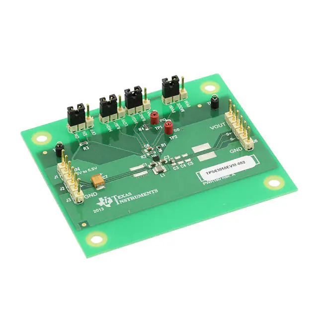
TPS6305xEVM-180
This user’s guide describes the characteristics, operation, and use of the TPS6305xEVM-180 evaluation
module (EVM). This EVM is designed to help the user easily evaluate and test the operation and
functionality of the TPS63050 and TPS63051. The EVM converts a 2.5-V to 5.5-V input voltage to a
regulated 3.3-V output voltage that delivers 500 mA. This document includes setup instructions for the
hardware, a schematic diagram, a bill of materials, and printed-circuit board layout drawings for the
evaluation module.
1
2
3
4
5
6
Contents
Introduction ..................................................................................................................
Setup .........................................................................................................................
Test Results .................................................................................................................
Board Layout ................................................................................................................
Schematic and Bill of Materials ...........................................................................................
Related Documentation From Texas Instruments ......................................................................
1
2
3
4
7
8
List of Figures
1
Thermal Performance (Vin = 5.5 V, Load = 500 mA) .................................................................. 3
2
Assembly Layer ............................................................................................................. 4
3
Top Layer Routing .......................................................................................................... 5
4
Bottom Layer Routing ...................................................................................................... 6
5
TPS6305xEVM-180 Schematic ........................................................................................... 7
List of Tables
1
1
Performance Specification Summary..................................................................................... 2
2
Current Limit Settings from ILIMx Pins ................................................................................... 3
3
TPS6305xEVM-180 Bill of Materials
.....................................................................................
8
Introduction
TI's TPS6305x are highly efficient, single-inductor, buck-boost converters with 1-A switches in a 1.6 mm ×
1.2 mm, 12-pin WCSP package. TPS63050 is an adjustable output voltage converter and TPS63051 is a
fixed 3.3-V output voltage converter.
1.1
Background
The TPS6305xEVM-180 uses either the TPS63050 adjustable version (PWR180-002) that is programmed
with an external feedback divider to an output voltage of 3.3-V or the TPS63051 fixed 3.3-V output voltage
version (PWR180-001). Both EVMs operate with an input voltage between 2.5-V and 5.5-V.
SLVU806 – July 2013
Submit Documentation Feedback
TPS6305xEVM-180
Copyright © 2013, Texas Instruments Incorporated
1
�Setup
1.2
www.ti.com
Performance Specification
Table 1 provides a summary of the TPS6305xEVM-180 performance specifications. All specifications are
given for operating in a free-air environment of an ambient temperature of 25°C.
Table 1. Performance Specification Summary
Specification
Test Conditions
Input voltage
Output voltage
Typ
2.5
PWM Mode
Output current
1.3
Min
3.267
0
3.3
Max
Unit
5.5
V
3.33
V
500
mA
Modifications
The printed-circuit board (PCB) for this EVM is designed to accommodate both the fixed and adjustable
versions of this integrated circuit (IC). If the fixed output voltage version (TPS63051) is installed, R1 is
replaced with a 0-Ω resistor and R2 is open. If the adjustable version (TPS63050) is installed, R1 and R2
are set per the datasheet.
2
Setup
This section describes how to properly use the TPS6305xEVM-180.
2.1
2.1.1
Input/Output Connector and Header Descriptions
J1 – VIN
This header is the positive connection to the input power supply. The power supply must be connected
between J1 and J3 (GND). The leads to the input supply should be twisted and kept as short as possible.
The input voltage has to be between 2.5 V and 5.5 V.
2.1.2
J2 – S+/S–
Header J2 can be used to measure the input voltage directly on the input capacitor. Therefore a 4-wire
power and sense supply can be connected. The leads to the sensing connector should also be twisted.
2.1.3
J3 – GND
This header is the return connection to the input power supply. Connect the power supply between J3 and
J1 (VIN). The leads to the input supply should be twisted and kept as short as possible. The input voltage
has to be between 2.5 V and 5.5 V.
2.1.4
J4 – VOUT
This header is the positive connection of the output voltage. The load has to be connected between J4
and J6 (GND).
2.1.5
J5 – S+/S–
Header J5 can be used to measure the output voltage directly on the output capacitor.
2.1.6
J6 – GND
This header is the return connection of the output voltage. Connect the load between J6 and J4 (VOUT).
2.1.7
JP1 – EN
This jumpers enable or disable the TPS6305x on the EVM. Place the jumper across ON and EN to enable
the converter. Place the jumper across OFF and EN to disable the converter. A 1-MΩ pullup resistor is
connected between VIN and EN. Removing the jumper on JP1 turns on the converter.
2
TPS6305xEVM-180
SLVU806 – July 2013
Submit Documentation Feedback
Copyright © 2013, Texas Instruments Incorporated
�Test Results
www.ti.com
2.1.8
JP2 – ILIM1
Together with JP3, this jumper controls the current limit of the TPS6305x. See Table 2.
2.1.9
JP3 – ILIM0
Together with JP2, this jumper controls the current limit of the TPS6305x. See Table 2.
Table 2. Current Limit Settings from ILIMx Pins
2.1.10
ILIM0
ILIM1
Current Limit Setting
(Typical)
Low
Low
200 mA
High
Low
300 mA
Low
High
500 mA
High
High
1A
JP4 – MODE
This jumpers control the operating mode of the TPS6305x on the EVM. Place the jumper across PWM
and MODE to enable forced PWM mode with a constant switching frequency. Place the jumper across
PFM and MODE to enable power save mode with higher efficiency.
2.1.11
TP1 – PG
This test point outputs the PG (power good) pin of the TPS6305x.
2.1.12
TP2 – SS
This test point outputs the SS (soft start) pin of the TPS6305x.
2.1.13
TP3/4 – GND
These test points are convenient ground connections.
2.2
Setup
To operate the EVM, simply connect an input supply between J1 and J3. Connect a load between J4 and
J6. An input supply voltage of 2.5 V to 5.5 V is recommended.
3
Test Results
The TPS6305xEVM-180 was used to take the data in the TPS6305x datasheet, SLVSAM8. See the
device datasheet for the performance of this EVM.
Figure 1. Thermal Performance (Vin = 5.5 V, Load = 500 mA)
SLVU806 – July 2013
Submit Documentation Feedback
TPS6305xEVM-180
Copyright © 2013, Texas Instruments Incorporated
3
�Board Layout
4
www.ti.com
Board Layout
This section provides the TPS63050xEVM-180 board layout and illustrations. The gerbers are available on
the EVM product page: TPS63051EVM-180.
4.1
Layout
Figure 2. Assembly Layer
4
TPS6305xEVM-180
SLVU806 – July 2013
Submit Documentation Feedback
Copyright © 2013, Texas Instruments Incorporated
�Board Layout
www.ti.com
Figure 3. Top Layer Routing
SLVU806 – July 2013
Submit Documentation Feedback
TPS6305xEVM-180
Copyright © 2013, Texas Instruments Incorporated
5
�Board Layout
www.ti.com
Figure 4. Bottom Layer Routing
6
TPS6305xEVM-180
SLVU806 – July 2013
Submit Documentation Feedback
Copyright © 2013, Texas Instruments Incorporated
�Schematic and Bill of Materials
www.ti.com
5
Schematic and Bill of Materials
This section provides the TPS6305xEVM-180 schematic and bill of materials.
5.1
Schematic
Figure 5 illustrates the schematic for this EVM.
L1
1.5uH
U1
TPS6305x
2.5V to 5.5V
A1 L1
VIN
J1
A2 VIN
VIN
A3 EN
R3
1M
J2
ON
S+
JP1
S-
+
J3
C7
OFF
47uF
GND
EN
C1
B3 ILIM1
10uF
C2 PFM/PWM
B1 GND
HIGH JP2
ILIM1
LOW
JP4
MODE
B2 ILIM0
2
L2 C1
ILIM0
LOW
R1
PG C3
2
C2
C3
C4
TP2 SS
3.3V, 500mA
10uF
10uF
C5
J5
1
1
S+
SS D3
SJ6
R2
C6
1000pF
TP3
J4
VOUT
FB D2
PWM
PFMHIGH
VOUT
VOUT D1
GND
2
TP4
JP3
VOUT
R4
1M
TP1
1
Not Populated
2
See BOM for component usage
PG
Figure 5. TPS6305xEVM-180 Schematic
SLVU806 – July 2013
Submit Documentation Feedback
TPS6305xEVM-180
Copyright © 2013, Texas Instruments Incorporated
7
�Related Documentation From Texas Instruments
5.2
www.ti.com
Bill of Materials
Table 3. TPS6305xEVM-180 Bill of Materials
6
-001
-002
RefDes
Value
Description
Size
Part Number
MFR
3
3
C1-3
10uF
Capacitor, Ceramic Chip, 6.3V, ±20%, X5R
0603
GRM188R60J106ME84
Murata
1
1
C6
1000pF
Capacitor, Ceramic Chip, 50V, ±10%, X5R
0603
CGA3E2X5R1H102K080AA
TDK
1
1
C7
47uF
Capacitor, Tantalum, 8V, 35milliohm, 20%
3528(B)
T520B476M008ATE035
Kemet
1
1
L1
1.5uH
Inductor, SMT ±30%
2520
1269AS-H-1R5M
Toko
1
0
R1
0
Resistor, Chip, 1/10W, 1%
0603
STD
STD
0
0
R2
Open
Resistor, Chip, 1/10W, 1%
0603
STD
STD
0
1
R1
560k
Resistor, Chip, 1/10W, 1%
0603
STD
STD
0
1
R2
180k
Resistor, Chip, 1/10W, 1%
0603
STD
STD
2
2
R3-4
1M
Resistor, Chip, 1/10W, 5%
0603
CRCW06031M00JNEA
Vishay
Dale
0
1
U1
--
IC, SINGLE INDUCTOR BUCK-BOOST WITH 1-A SWITCHES AND
ADJUSTABLE SOFT START
BGA
TPS63050YFF
TI
1
0
U1
--
IC, SINGLE INDUCTOR BUCK-BOOST WITH 1-A SWITCHES AND
ADJUSTABLE SOFT START
BGA
TPS63051YFF
TI
Related Documentation From Texas Instruments
Single Inductor Buck-Boost with 1-A Switches and Adjustable Soft Start datasheet (SLVSAM8)
8
TPS6305xEVM-180
SLVU806 – July 2013
Submit Documentation Feedback
Copyright © 2013, Texas Instruments Incorporated
�IMPORTANT NOTICE
Texas Instruments Incorporated and its subsidiaries (TI) reserve the right to make corrections, enhancements, improvements and other
changes to its semiconductor products and services per JESD46, latest issue, and to discontinue any product or service per JESD48, latest
issue. Buyers should obtain the latest relevant information before placing orders and should verify that such information is current and
complete. All semiconductor products (also referred to herein as “components”) are sold subject to TI’s terms and conditions of sale
supplied at the time of order acknowledgment.
TI warrants performance of its components to the specifications applicable at the time of sale, in accordance with the warranty in TI’s terms
and conditions of sale of semiconductor products. Testing and other quality control techniques are used to the extent TI deems necessary
to support this warranty. Except where mandated by applicable law, testing of all parameters of each component is not necessarily
performed.
TI assumes no liability for applications assistance or the design of Buyers’ products. Buyers are responsible for their products and
applications using TI components. To minimize the risks associated with Buyers’ products and applications, Buyers should provide
adequate design and operating safeguards.
TI does not warrant or represent that any license, either express or implied, is granted under any patent right, copyright, mask work right, or
other intellectual property right relating to any combination, machine, or process in which TI components or services are used. Information
published by TI regarding third-party products or services does not constitute a license to use such products or services or a warranty or
endorsement thereof. Use of such information may require a license from a third party under the patents or other intellectual property of the
third party, or a license from TI under the patents or other intellectual property of TI.
Reproduction of significant portions of TI information in TI data books or data sheets is permissible only if reproduction is without alteration
and is accompanied by all associated warranties, conditions, limitations, and notices. TI is not responsible or liable for such altered
documentation. Information of third parties may be subject to additional restrictions.
Resale of TI components or services with statements different from or beyond the parameters stated by TI for that component or service
voids all express and any implied warranties for the associated TI component or service and is an unfair and deceptive business practice.
TI is not responsible or liable for any such statements.
Buyer acknowledges and agrees that it is solely responsible for compliance with all legal, regulatory and safety-related requirements
concerning its products, and any use of TI components in its applications, notwithstanding any applications-related information or support
that may be provided by TI. Buyer represents and agrees that it has all the necessary expertise to create and implement safeguards which
anticipate dangerous consequences of failures, monitor failures and their consequences, lessen the likelihood of failures that might cause
harm and take appropriate remedial actions. Buyer will fully indemnify TI and its representatives against any damages arising out of the use
of any TI components in safety-critical applications.
In some cases, TI components may be promoted specifically to facilitate safety-related applications. With such components, TI’s goal is to
help enable customers to design and create their own end-product solutions that meet applicable functional safety standards and
requirements. Nonetheless, such components are subject to these terms.
No TI components are authorized for use in FDA Class III (or similar life-critical medical equipment) unless authorized officers of the parties
have executed a special agreement specifically governing such use.
Only those TI components which TI has specifically designated as military grade or “enhanced plastic” are designed and intended for use in
military/aerospace applications or environments. Buyer acknowledges and agrees that any military or aerospace use of TI components
which have not been so designated is solely at the Buyer's risk, and that Buyer is solely responsible for compliance with all legal and
regulatory requirements in connection with such use.
TI has specifically designated certain components as meeting ISO/TS16949 requirements, mainly for automotive use. In any case of use of
non-designated products, TI will not be responsible for any failure to meet ISO/TS16949.
Products
Applications
Audio
www.ti.com/audio
Automotive and Transportation
www.ti.com/automotive
Amplifiers
amplifier.ti.com
Communications and Telecom
www.ti.com/communications
Data Converters
dataconverter.ti.com
Computers and Peripherals
www.ti.com/computers
DLP® Products
www.dlp.com
Consumer Electronics
www.ti.com/consumer-apps
DSP
dsp.ti.com
Energy and Lighting
www.ti.com/energy
Clocks and Timers
www.ti.com/clocks
Industrial
www.ti.com/industrial
Interface
interface.ti.com
Medical
www.ti.com/medical
Logic
logic.ti.com
Security
www.ti.com/security
Power Mgmt
power.ti.com
Space, Avionics and Defense
www.ti.com/space-avionics-defense
Microcontrollers
microcontroller.ti.com
Video and Imaging
www.ti.com/video
RFID
www.ti-rfid.com
OMAP Applications Processors
www.ti.com/omap
TI E2E Community
e2e.ti.com
Wireless Connectivity
www.ti.com/wirelessconnectivity
Mailing Address: Texas Instruments, Post Office Box 655303, Dallas, Texas 75265
Copyright © 2015, Texas Instruments Incorporated
�


 工商网监
湘ICP备2023018690号
工商网监
湘ICP备2023018690号
