User's Guide
SLVUAD6 – December 2014
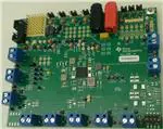
TPS650830EVM-095
The TPS650830EVM-095 evaluation module is a fully assembled and tested circuit for evaluating the
TPS650830 6-channel power management integrated circuit. The TPS650830EVM provides a platform for
a user or designer to evaluate the TPS650830. It has the capabilities to experiment with the part in a
holistic design approach for computing power and in a generic mode such as if the TPS650830 is placed
into a new experimental application. This document includes instructions and results of typical electrical
performance characteristics, connector and test point descriptions, setup instructions, schematics, printedcircuit-board (PCB) layouts and the bill of materials (BOM). Throughout this user's guide, the abbreviations
EVM, TPS650830EVM, and the term evaluation module are synonymous with the TPS650830EVM-095,
unless otherwise noted.
1
2
3
4
5
6
7
Contents
Introduction ................................................................................................................... 2
1.1
Features .............................................................................................................. 2
1.2
Applications .......................................................................................................... 2
1.3
Requirements ....................................................................................................... 2
TPS65083xEVM Electrical Performance Specifications ................................................................ 3
TPS650830EVM Schematics .............................................................................................. 5
3.1
TPS650830 Voltage Rails ......................................................................................... 5
3.2
TPS650830 Controls and TPS650830 Features ............................................................... 7
3.3
Discretes and POLs ................................................................................................ 9
Connectors, Switches and Test Point Descriptions .................................................................... 10
4.1
Power Connections ............................................................................................... 10
4.2
Switches ............................................................................................................ 10
4.3
Enables ............................................................................................................. 10
Setup ......................................................................................................................... 11
5.1
Hardware Setup ................................................................................................... 11
5.2
Software Setup .................................................................................................... 11
5.3
Running the Software ............................................................................................. 12
TPS65083xEVM Assembly Drawings and Layout ..................................................................... 14
Bill of Materials ............................................................................................................. 18
List of Figures
.............................................................................. 5
.............................................................................. 5
TPS650830EVM VR5 and LDO1 Schematic............................................................................. 6
TPS650830EVM VR Outputs Schematic ................................................................................. 6
TPS650830EVM Controls Schematic .................................................................................... 7
TPS650830EVM TPS650830 Schematic ................................................................................. 8
TPS650830EVM Discretes and POLs Schematic ....................................................................... 9
Hardware Board Connection .............................................................................................. 11
Firmware Update Required Message.................................................................................... 12
Software Overview ......................................................................................................... 12
TPS65083xEVM Component Placement (Viewed From Top)........................................................ 14
TPS65083xEVM Bottom Component Placement (X-Ray View) ..................................................... 15
TPS65083xEVM Top Copper (Viewed From Top) ..................................................................... 15
1
TPS650830EVM VR1 and VR2 Schematic
2
TPS650830EVM VR3 and VR4 Schematic
3
4
5
6
7
8
9
10
11
12
13
SLVUAD6 – December 2014
Submit Documentation Feedback
TPS650830EVM-095
Copyright © 2014, Texas Instruments Incorporated
1
�Introduction
www.ti.com
14
TPS65083xEVM GND Layer (X-Ray View From Top) ................................................................ 15
15
TPS65083xEVM Signal 1 (X-Ray View From Top) .................................................................... 16
16
TPS65083xEVM Multi 1 (X-Ray View From Top) ...................................................................... 16
17
TPS65083xEVM Multi 2 (X-Ray View From Top) ...................................................................... 16
18
TPS65083xVM Signal 2 (X-Ray View From Top) ...................................................................... 16
19
TPS65083xEVM Power Layer (X-Ray View From Top)
20
..............................................................
TPS65083xEVM Bottom Copper (X-Ray View) ........................................................................
17
17
List of Tables
1
2
3
.......................................................... 3
Output Rail Headers ....................................................................................................... 10
HPA515B Bill of Materials ................................................................................................. 18
TPS650830EVM Electrical and Performance Specifications
1
Introduction
1.1
Features
•
•
•
•
•
•
•
•
•
•
•
•
•
1.3
4 DCAP2™ Controllers
1 Converter, 2-MHz Switching Frequency
DDR Termination LDO, ±1 A
Wide Vin Range, 5.4 V – 21 V
Dynamic Voltage Scaling, via I2C and/or
Hardware Signal
Output voltage adjustable via I2C interface
Power Path Management for 2 Batteries and
1 Adaptor
8 Power Good Comparators and Sequence
Logic for External DCDCs, LDOs and Load
Switches.
2 Level Shifters
Power-Button Logic Supported with
Programable Response Time and Counter
Reporting
RTC Backup Battery Selector with 3.1-V
LDO Output
Board Temperature Monitoring System
1-Hz Wake EC Clock
To operate the EVM for basic evaluation
purposes a PC, the EVM software, and power
supply are needed in addition to basic a
voltmeter or Digital Multimeter, DMM.
1.3.1
Applications
•
•
•
•
•
Host Computer
A personal computer (PC) with a USB port is
required to operate this EVM. The TPS65083x
software runs on the PC and communicates
with the EVM via the PC's USB port and the
USB-to-GPIO interface.
PC Requirements :
• Microsoft® Windows® 7 operating system
• USB port
• Minimum of 30MB of free hard-disk space
(100MB recommended)
• Minimum of 256MB of RAM
1.3.2
Software
Download and install the TPS65083xEVM GUI
on a PC to access the I2C registers.
1.3.3
1.2
Requirements
Power Supply Requirements
A DC power supply capable of delivering up to
21 V, 9 A, and 50 W is required to operate this
EVM to its max power outputs.
Notebook Computing
Tablets
Human Machine Interface
Infotainment Systems
FPGA System Power
Microsoft, Windows are registered trademarks of Microsoft Corporation.
2
TPS650830EVM-095
SLVUAD6 – December 2014
Submit Documentation Feedback
Copyright © 2014, Texas Instruments Incorporated
�TPS65083xEVM Electrical Performance Specifications
www.ti.com
2
TPS65083xEVM Electrical Performance Specifications
Table 1. TPS650830EVM Electrical and Performance Specifications
Parameter
Symbol
Notes and Conditions
Min
Typ
Max
Unit
Input Characteristics
Input voltage
VBATA
VIN
Input Current
IBATA
UVLO
VUVLO
VIN falling
VHYS-UVLO
VIN rising
UVLO hysteresis
5.4
0
4.95
5.1
21
V
9
A
5.25
200
V
mV
Output Characteristics
VR1
Output voltage VR1
VR1, V1.00A
1.0V
I2C Programmable Range Margining
Output voltage accuracy VR1
-5
-1
Load Regulation
Output Current VR1
V
+5
%
1
%
0.5
IOUT,
VR1
VIN = Min to Max, Low Side RdsON =
7mΩ, Rcs = 9.53 kΩ, L = 1 µH
%
6.8
A
Current Limit Low-Side MOSFET
ILIMF
Low Side RdsON = 7mΩ, Rcs = 9.53
kΩ
8.5
A
Switching frequency
FSW
NVDCZ = HIGH
500
kHz
VR2
Output voltage VR2
VR2, V1.8A
1.8V
I2C Programmable Range Margining
Output voltage accuracy VR2
-4
-1
Load Regulation
Output Current VR2
Switching frequency
V
+3
%
1
%
0.5
IOUT,
VR2
VIN = Min to Max
%
1.8
A
FSW
2000
kHz
VR3,
V3.3A_DSW
3.3V
V
VR3
Output voltage VR3
I2C Programmable Range Margining
Output voltage accuracy VR3
-4
+3
%
-1
1
%
Load Regulation
Output Current VR3
0.5
IOUT,
VR3
VIN = Min to Max, Low Side RdsON =
7mΩ, High Side RdsON = 15.7mΩ, Rcs
= 8.66 kΩ, L = 1.5 µH
Current Limit High-Side MOSFET
ILIMF
High Side RdsON = 15.7mΩ, Rcs (HS) =
22.6 kΩ, L = 1.5 µH, VIN up to 9V
Current Limit Low-Side MOSFET
ILIMF
Switching frequency
FSW
%
6.6
A
13.15
A
Low Side RdsON = 7mΩ, Rcs = 8.66
kΩ
7.73
A
NVDCZ = HIGH
800
kHz
VR4
Output voltage VR4
VR4, VDDQ
DDRID shorted to GND
I2C Programmable Range Margining
Output voltage accuracy VR4
-1
Load Regulation
Switching frequency
Output Current VR4
1.2V
-4
FSW
IOUT,
VR4
V
+3
%
1
%
0.5
%
500
kHz
VIN = Min to Max, Low Side RdsON =
7mΩ, Rcs = 10.5 kΩ, L = 1 µH
7.47
A
Current Limit Low-Side MOSFET
ILIMF
Low Side RdsON = 7mΩ, Rcs = 10.5
kΩ
9.38
A
Switching frequency
FSW
NVDCZ = HIGH
500
kHz
SLVUAD6 – December 2014
Submit Documentation Feedback
TPS650830EVM-095
Copyright © 2014, Texas Instruments Incorporated
3
�TPS65083xEVM Electrical Performance Specifications
www.ti.com
Table 1. TPS650830EVM Electrical and Performance Specifications (continued)
Parameter
Symbol
Notes and Conditions
Min
Typ
Max
Unit
VR5
Output voltage VR5
VR5, V5A_DS3
5V
I2C Programmable Range Margining
Output voltage accuracy VR5
-4
-1
Load Regulation
Output Current VR5
V
+3
%
1
%
0.5
IOUT,
VR5
VIN = Min to Max, Low Side RdsON =
7mΩ, High Side RdsON = 15.7mΩ, Rcs
= 4.87 kΩ, L = 3.3 µH
%
3.55
A
Current Limit High-Side MOSFET
ILIMF
High Side RdsON = 15.7mΩ, Rcs (HS) =
10.2 kΩ, L = 3.3 µH, VIN up to 9V
6.83
A
Current Limit Low-Side MOSFET
ILIMF
Low Side RdsON = 7mΩ, Rcs = 4.87
kΩ
4.35
A
Switching frequency
FSW
NVDCZ = HIGH
800
kHz
0.6V
V
LDO1
Output voltage LDO1
VLDO1, VTT
DDRID shorted to GND, VR4/VDDQ
supplies VINLDO1 = 1.2V
Output current of LDO1
-1
Source Current Limit of LDO1
Sink Current Limit of LDO1
4
1
2
A
-2
TPS650830EVM-095
A
A
SLVUAD6 – December 2014
Submit Documentation Feedback
Copyright © 2014, Texas Instruments Incorporated
�TPS650830EVM Schematics
www.ti.com
3
TPS650830EVM Schematics
3.1
TPS650830 Voltage Rails
Figure 1. TPS650830EVM VR1 and VR2 Schematic
Figure 2. TPS650830EVM VR3 and VR4 Schematic
SLVUAD6 – December 2014
Submit Documentation Feedback
TPS650830EVM-095
Copyright © 2014, Texas Instruments Incorporated
5
�TPS650830EVM Schematics
www.ti.com
Figure 3. TPS650830EVM VR5 and LDO1 Schematic
Figure 4. TPS650830EVM VR Outputs Schematic
6
TPS650830EVM-095
SLVUAD6 – December 2014
Submit Documentation Feedback
Copyright © 2014, Texas Instruments Incorporated
�TPS650830EVM Schematics
www.ti.com
3.2
TPS650830 Controls and TPS650830 Features
Figure 5. TPS650830EVM Controls Schematic
SLVUAD6 – December 2014
Submit Documentation Feedback
TPS650830EVM-095
Copyright © 2014, Texas Instruments Incorporated
7
�TPS650830EVM Schematics
www.ti.com
Figure 6. TPS650830EVM TPS650830 Schematic
8
TPS650830EVM-095
SLVUAD6 – December 2014
Submit Documentation Feedback
Copyright © 2014, Texas Instruments Incorporated
�TPS650830EVM Schematics
www.ti.com
3.3
Discretes and POLs
Figure 7. TPS650830EVM Discretes and POLs Schematic
SLVUAD6 – December 2014
Submit Documentation Feedback
TPS650830EVM-095
Copyright © 2014, Texas Instruments Incorporated
9
�Connectors, Switches and Test Point Descriptions
www.ti.com
4
Connectors, Switches and Test Point Descriptions
4.1
Power Connections
4.1.1
J1 – VIN
This header is the positive connection to the input power supply. The power supply must be connected
between J1 and J2 (GND). The leads to the input supply must be kept as short as possible. The input
voltage has to be between 5.4 V and 21 V.
4.1.2
J2 – GND
This header is the return connection to the input power supply for GND.
4.1.3
Output Voltage Rails
See Table 2 for header names, power source descriptions, and sequence.
Table 2. Output Rail Headers
4.2
4.2.1
Header
Name
J6
J7
Source
Turns On With
TPS650830EVM
TPS650831EVM
TPS650832EVM
V3.3_DSW
VR3
POL, Discrete
VR3
V1.8A
VR2
VR5
VR2
Valid VIN
J10
V5A_DS3
VR5
POL, Discrete
VR5
SLP_SUS# Asserts Hign
J11
V3.3A_PCH
POL, Load
Switch
POL, Load Switch
POL, Load Switch
SLP_SUS# Asserts Hign
J14
V0.85A
VR1
VR2
POL, Discrete
SLP_SUS# Asserts Hign
J15
V1.00A
VR1
VR1
VR1
SLP_SUS# Asserts Hign
J16
VDDQ
VR4
VR4
VR4
SLP_S4# Asserts Hign
J19
V1.8U_2.5U
POL, Load
Switch
POL, Load Switch
POL, Load Switch
SLP_S4# Asserts Hign
J20
VCCIO
POL, Load
Switch
VR3
POL, Discrete
SLP_S3# Asserts Hign
J23
VTT
VLDO1
VLDO1
VLDO1
SLP_S0# Asserts Hign
Valid VIN
Switches
S1 – PB_IN
This is the pushbutton input. Pressing S1 pulls PWRBTNIN to GND. The power button can be used for
many features such as turn on after a RESET or causing a RESET if configured correct via I2C. See the
datasheet for more options and uses of the power button.
4.2.2
S2 – Multi-Switch Shutdown, NVDC, and 3.3-V Load Switch
This switch has 4 dip switches in it. Switch 1 is unused. Switch 2 is internal 3.3-V load switch enable. Set
away from the ON position to enable the internal 3.3-V load switch. Switch 3 is NVDC selector. Set
towards the ON position to put the device into NVDC mode. Switch 4 is Shutdown mode. Set towards the
ON position to put the device into SHUTDOWN mode.
4.3
Enables
There are places for jumpers to enable the VRs directly on the board. However, the TPS650830EVM has
other jumpers that set the Sleep States for the device. The sleep states indirectly enable the VRs.
VR2 and VR3 are already on before any enable switch asserting high. They are enabled by DPWROK and
LDO3, respectively, with LDO3 enabled when VIN > UVLO.
10
TPS650830EVM-095
SLVUAD6 – December 2014
Submit Documentation Feedback
Copyright © 2014, Texas Instruments Incorporated
�Setup
www.ti.com
4.3.1
J4 - SLP_SUS#
SLP_SUS# is active low and when set low will put the device into sleep state SUSPEND. When
SLP_SUS# asserts high, VR5 and VR1 turn on as well as the device enabling a load switch.
4.3.2
J4 - SLP_S4#
SLP_S4# is active low and when set low will put the device into sleep state 4. When SLP_4# asserts high,
VR4 turns on as well as the device enabling a load switch.
4.3.3
J4 - SLP_S3#
SLP_S3# is active low and when set low will put the device into sleep state 3. When SLP_3# asserts high,
the device enables a load switch.
4.3.4
J4 - SLP_S0#
SLP_S0# is active low and when set low will put the device into sleep state 0. When SLP_0# asserts high,
VLDO1 turns on.
5
Setup
5.1
Hardware Setup
x
x
x
x
Green LED
x
x
USB to ANY Interface
USB / miniUSB
Cable
Ribbon
Cable
x
x
PC
J32
TPS65083xEVM-095
Any VR
J1
Load for Testing
J2
Power Supply
Figure 8. Hardware Board Connection
Before connecting the EVM, always remember to preset the power supply to correct voltages. Never "hot
plug" or connect the power supply to the EVM with the power supply on. This can result in 2x input voltage
overshoot that can damage the devices on the EVM.
Connect the EVM as shown in Figure 8. Before turning on the power supply, set the SLP_Sx# jumpers to
LOW as they must be sequenced in the proper order for correct power up. The order for sequence is
SLP_SUS# → SLP_S4# → SLP_S3# → SLP_S0#.
Once the power supply is on and providing a valid VIN voltage, the SLP_Sx# signal can be set to HIGH in
the listed sequence. After this, the EVM will have all power rails ON and regulating to their set voltage.
ALL_SYS_PWRGD, TP71, should be HIGH signaling a valid power up of the system.
5.2
Software Setup
To install the GUI, first download the GUI from the Tools & Software folder at
http://www.ti.com/product/TPS650830/toolssoftware. Once the zip file is open, simply double-click the
Setup TPS65083xEVM.msi file. Follow the recommended prompts for installation.
SLVUAD6 – December 2014
Submit Documentation Feedback
TPS650830EVM-095
Copyright © 2014, Texas Instruments Incorporated
11
�Setup
www.ti.com
Once installed, the GUI appears as seen in Figure 10.
It is possible that first running the GUI and therefore the USB2GUI box, that the user will have to update
the USB2ANY box’s firmware. If this is the case, the user will receive a message similar to Figure 9.
Figure 9. Firmware Update Required Message
5.3
Running the Software
Click on the TPS65083xEVM icon to start the software. If no icon appears on the host computer, then use
the start button in the lower left corner of the screen to browse the program folders to find the software.
The default directory for software installation is Program Files\Texas Instruments\TPS65083xEVM.
Figure 10 is a diagram of the GUI and beneath the figure are descriptions of each feature that the GUI has
to offer. The GUI has register and bit names. The register name is listed to the left of the data and I2C
addresses. To see the bit names, hover the mouse over the data bit and the bit name will appear for as
long as the mouse is positioned over the bit. See the TPS65083x data sheet for detailed description on
these registers.
Figure 10. Software Overview
12
TPS650830EVM-095
SLVUAD6 – December 2014
Submit Documentation Feedback
Copyright © 2014, Texas Instruments Incorporated
�Setup
www.ti.com
•
•
•
•
•
•
(A) = USB2ANY Detection – If this message reads “USB2ANY Detected”, then the GUI and USB2ANY
are operating correctly in that they are communicating to one another.
– If this message reads “USB2ANY Not Detected” then the GUI and USB2ANY are not operating
correctly and communication needs to be established. Try unplugging the USB cable, shutting
down and restarting the GUI, followed by plugging in the USB cable.
(B) = I2C Address Selection – Select the desired I2C address before attempting to communicate. The
TPS65083x operates on 1 of 3 addresses: x30, x32, or x34, depending on the hardware configuration
of SLAVEADDR pin.
(C) = Read and Write All Commands – Use read and write all commands to read or write data on all
the registers featured in the REGISTER List.
(D) = File – User can select to save or load registers to or from a .txt file.
(E) = I2C Activity – Logs all user activity over the I2C communication bus since opening the GUI or
since last “Clear”. User can clear activity log by clicking on the “Clear” button.
(F) = Auto Read – User can select to read all registers or just a single register every 1, 5, 10, or 20
seconds, as desired.
SLVUAD6 – December 2014
Submit Documentation Feedback
TPS650830EVM-095
Copyright © 2014, Texas Instruments Incorporated
13
�TPS65083xEVM Assembly Drawings and Layout
6
www.ti.com
TPS65083xEVM Assembly Drawings and Layout
Figure 11 through Figure 18 show the design of the TPS65083xEVM printed-circuit board.
Figure 11. TPS65083xEVM Component Placement (Viewed From Top)
14
TPS650830EVM-095
SLVUAD6 – December 2014
Submit Documentation Feedback
Copyright © 2014, Texas Instruments Incorporated
�TPS65083xEVM Assembly Drawings and Layout
www.ti.com
Figure 12. TPS65083xEVM Bottom Component Placement (X-Ray View)
SLVUAD6 – December 2014
Submit Documentation Feedback
TPS650830EVM-095
Copyright © 2014, Texas Instruments Incorporated
15
�TPS65083xEVM Assembly Drawings and Layout
16
www.ti.com
Figure 13. TPS65083xEVM Top Copper
(Viewed From Top)
Figure 14. TPS65083xEVM GND Layer
(X-Ray View From Top)
Figure 15. TPS65083xEVM Signal 1
(X-Ray View From Top)
Figure 16. TPS65083xEVM Multi 1
(X-Ray View From Top)
TPS650830EVM-095
SLVUAD6 – December 2014
Submit Documentation Feedback
Copyright © 2014, Texas Instruments Incorporated
�TPS65083xEVM Assembly Drawings and Layout
www.ti.com
Figure 17. TPS65083xEVM Multi 2
(X-Ray View From Top)
Figure 18. TPS65083xVM Signal 2
(X-Ray View From Top)
Figure 19. TPS65083xEVM Power Layer
(X-Ray View From Top)
Figure 20. TPS65083xEVM Bottom Copper
(X-Ray View)
SLVUAD6 – December 2014
Submit Documentation Feedback
TPS650830EVM-095
Copyright © 2014, Texas Instruments Incorporated
17
�Bill of Materials
7
www.ti.com
Bill of Materials
Table 3 lists the BOM.
Table 3. HPA515B Bill of Materials
Designator
Quantity
Value
Description
Package Reference
Part Number
Manufacturer
C1
1
47uF
CAP, TA, 47 µF, 35 V, +/- 10%, 0.3 ohm, SMD
7343-43
T495X476K035ATE300
Kemet
C3, C4, C17, C18, C24, C25, C32, C33
8
10uF
CAP, CERM, 10 µF, 25 V, +/- 10%, X5R, 0805_140
0805_140
GRM21BR61E106KA73L
MuRata
C5, C11, C12, C26
4
1uF
CAP, CERM, 1 µF, 10 V, +/- 10%, X5R, 0603
0603
GRM188R61A105KA61D
MuRata
C6, C19, C20, C21, C27, C34, C35,
C36, C37, C38, C39, C40, C41
13
100uF
CAP, CERM, 100 µF, 6.3 V, +/- 20%, X5R, 0805_140
0805_140
GRM21BR60J107M
MuRata
C7
1
220uF
CAP, CERM, 220 µF, 4 V, +/- 20%, X5R, 1206_190
1206
GRM31CR60G227ME11
Murata
C8, C9, C28, C29
4
220uF
CAP, CERM, 220 µF, 4 V, +/- 20%, X5R, 1206_190
1206_190
GRM31CR60G227ME11L
MuRata
C10, C23, C31, C42
4
0.1uF
CAP, CERM, 0.1 µF, 10 V, +/- 10%, X5R, 0402
0402
C1005X5R1A104K
TDK
C13, C14, C15, C16, C43
5
47uF
CAP, CERM, 47 µF, 6.3 V, +/- 20%, X5R, 0603
0603
GRM188R60J476M
MuRata
C45
1
10uF
CAP, CERM, 10uF, 6.3V, +/-20%, X5R, 0402
0402
GRM155R60J106ME44
MuRata
C46
1
2.2uF
CAP, CERM, 2.2 µF, 6.3 V, +/- 20%, X5R, 0402
0402
GRM155R60J225ME15D
MuRata
C47
1
0.22uF
CAP, CERM, 0.22 µF, 6.3 V, +/- 20%, X5R, 0402
0402
C1005X5R0J224M
TDK
C48, C57, C58, C59, C60
5
1uF
CAP, CERM, 1 µF, 50 V, +/- 10%, X5R, 0603
0603
GRM188R61H105KAALD
MuRata
C49
1
10uF
CAP, CERM, 10 µF, 10 V, +/- 20%, X5R, 0603
0603
C1608X5R1A106M
TDK
C51
1
4.7uF
CAP, CERM, 4.7 µF, 10 V, +/- 10%, X5R, 0603
0603
CGB3B1X5R1A475K055AC
TDK
C52, C65, C68, C74
4
0.1uF
CAP, CERM, 0.1 µF, 6.3 V, +/- 10%, X5R, 0402
0402
C1005X5R0J104K
TDK
C53
1
0.47uF
CAP, CERM, 0.47 µF, 6.3 V, +/- 10%, X5R, 0402
0402
GRM155R60J474KE19D
MuRata
C54, C56, C64, C67, C73
5
1uF
CAP, CERM, 1 µF, 6.3 V, +/- 20%, X5R, 0402
0402
C1005X5R0J105M
TDK
D1, D2, D3
3
30V
Diode, Schottky, 30 V, 0.2 A, SOT-23
SOT-23
BAT54-7-F
Diodes Inc.
H1, H2, H3, H4, H5, H6
6
Bumpon, Cylindrical, 0.312 X 0.200, Black
Black Bumpon
SJ61A1
3M
J1
1
10A
Standard Banana Jack, insulated, 10A, red
571-0500
571-0500
DEM Manufacturing
J2
1
10A
Standard Banana Jack, insulated, 10A, black
571-0100
571-0100
DEM Manufacturing
J3
1
Header, 100mil, 6x1, Gold, TH
6x1 Header
TSW-106-07-G-S
Samtec
J4, J8, J12, J17, J21, J34
6
Header, 100mil, 3x1, Tin, TH
Header, 3x1, 100mil, TH
5-146278-3
TE Connectivity
J6, J7, J10, J11, J14, J15, J16, J19, J20,
J23
10
Terminal Block, 2-pole, 200mil, TH
THD, 2-Leads, Body
10.16x7.6mm, Pitch
5.08mm
OSTTC022162
On-Shore Technology
J24, J25, J33
3
Header, 100mil, 8x2, Gold, TH
8x2 Header
TSW-108-07-G-D
Samtec
J26
1
Header, 100mil, 8x1, Tin, TH
Header, 8x1, 100mil, TH
5-146278-8
TE Connectivity
J27, J28, J29, J30, J31, J35
6
Header, 100mil, 2x1, Tin, TH
Header, 2x1, 100mil, TH
5-146278-2
TE Connectivity
J32
1
Header (shrouded), 100mil, 5x2, High-Temperature, Gold, TH
5x2 Shrouded header
N2510-6002-RB
3M
L1
1
1uH
Inductor, Drum Core, Powdered Iron, 1 µH, 8 A, 0.015 ohm, SMD
Inductor, 5.2x1.6x5.2mm
PIMB051H-1R0MS
Cyntec
L2
1
680nH
Inductor, Drum Core, Powdered Iron, 680 nH, 4.3 A, 0.027 ohm,
SMD
Inductor, 3.2x1.2x2.5mm
PIFE32251B-R68MS-63
Cyntec
L3
1
1.5uH
Inductor, Drum Core, Powdered Iron, 1.5 µH, 6.5 A, 0.02 ohm, SMD
7.05 x 1.6 x 6.6mm
PIMB061H-1R5MS
Cyntec
L4
1
1uH
Inductor, Drum Core, Powdered Iron, 1 µH, 8.1 A, 0.014 ohm, SMD
Inductor, 5.2x1.6x5.2mm
PIME051H-1R0MS-63
Cyntec
L5
1
3.3uH
Inductor, Drum Core, Powdered Iron, 3.3 µH, 4.5 A, 0.052 ohm, SMD
Inductor, 5.2x1.6x5.2mm
PIMB051H-3R3MS
Cyntec
LBL1
1
Thermal Transfer Printable Labels, 0.650" W x 0.200" H - 10,000 per
roll
PCB Label 0.650"H x
0.200"W
THT-14-423-10
Brady
18
TPS650830EVM-095
SLVUAD6 – December 2014
Submit Documentation Feedback
Copyright © 2014, Texas Instruments Incorporated
�Bill of Materials
www.ti.com
Table 3. HPA515B Bill of Materials (continued)
Designator
Quantity
Description
Package Reference
Part Number
Manufacturer
Q1, Q2, Q3, Q4
4
Value
Synchronous Buck NexFET Power Block II, MPC0005A
MPC0005A
CSD87381P
Texas Instruments
Q5, Q6
2
5.5-V, 6-A, 4.4-mO On-Resistance Load Switch, DNY0008A
DNY0008A
TPS22969DNY
Texas Instruments
Q7
1
3.5-V, 6-A, Ultra-low Resistance Load Switch, DNY0008A
DNY0008A
TPS22961DNYR
Texas Instruments
R1, R3, R15, R16, R29, R32, R50, R58,
R59, R75, R201
11
0.002
RES, 0.002, 2%, 1 W, 0508
0508
KRL2012E-M-R002-G-T5
Susumu Co Ltd
R2, R4, R5, R6, R7, R8, R9, R10, R12,
R18, R19, R20, R23, R26, R27, R35,
R36, R37, R40, R41, R46, R51, R52,
R53, R54, R55, R61, R62, R63, R64,
R66, R67, R70, R73, R77, R86, R87,
R89, R91, R92, R96, R97, R98, R101,
R103, R104, R114, R115, R116, R119,
R121, R122, R123, R125, R133, R134,
R142, R143, R144, R159, R162, R165,
R166, R173, R174, R199, R200, R202,
R204, R206, R207
71
0
RES, 0, 5%, 0.063 W, 0402
0402
CRCW04020000Z0ED
Vishay-Dale
R13
1
9.53k
RES, 9.53 k, 1%, 0.063 W, 0402
0402
CRCW04029K53FKED
Vishay-Dale
R22
1
100
RES, 100, 5%, 0.063 W, 0402
0402
CRCW0402100RJNED
Vishay-Dale
R33
1
0
RES, 0, 5%, 0.1 W, 0603
0603
CRCW06030000Z0EA
Vishay-Dale
R44, R57, R105, R106, R107, R108,
R109, R110, R111, R112, R113, R127,
R128, R130, R131, R137, R138, R140,
R149, R150, R151
21
100k
RES, 100 k, 5%, 0.063 W, 0402
0402
CRCW0402100KJNED
Vishay-Dale
R45
1
22.6k
RES, 22.6 k, 1%, 0.063 W, 0402
0402
CRCW040222K6FKED
Vishay-Dale
R47
1
8.66k
RES, 8.66 k, 1%, 0.063 W, 0402
0402
CRCW04028K66FKED
Vishay-Dale
R56
1
10.5k
RES, 10.5 k, 1%, 0.063 W, 0402
0402
CRCW040210K5FKED
Vishay-Dale
R71
1
10.2k
RES, 10.2 k, 1%, 0.063 W, 0402
0402
CRCW040210K2FKED
Vishay-Dale
R72
1
4.87k
RES, 4.87 k, 1%, 0.063 W, 0402
0402
CRCW04024K87FKED
Vishay-Dale
R124
1
0
RES, 0, 5%, 0.125 W, 0805
0805
CRCW08050000Z0EA
Vishay-Dale
R126
1
10k
RES, 10 k, 5%, 0.063 W, 0402
0402
CRCW040210K0JNED
Vishay-Dale
R132
1
51
RES, 51, 5%, 0.063 W, 0402
0402
CRCW040251R0JNED
Vishay-Dale
R136
1
1.00Meg
RES, 1.00 M, 1%, 0.063 W, 0402
0402
CRCW04021M00FKED
Vishay-Dale
R139
1
200k
Trimmer, 200 K, 0.5 W, TH
Thumbwheel Trimmer
3352P-1-204LF
Bourns
R141
1
1.0k
RES, 1.0 k, 5%, 0.063 W, 0402
0402
CRCW04021K00JNED
Vishay-Dale
R146
1
267k
RES, 267 k, 1%, 0.063 W, 0402
0402
CRCW0402267KFKED
Vishay-Dale
R147, R148
2
237k
RES, 237 k, 1%, 0.063 W, 0402
0402
CRCW0402237KFKED
Vishay-Dale
R152
1
31.6k
RES, 31.6 k, 1%, 0.063 W, 0402
0402
CRCW040231K6FKED
Vishay-Dale
R153, R154
2
61.9k
RES, 61.9 k, 1%, 0.063 W, 0402
0402
CRCW040261K9FKED
Vishay-Dale
R205
1
249k
RES, 249 k, 1%, 0.063 W, 0402
0402
CRCW0402249KFKED
Vishay-Dale
RT1, RT2, RT3, RT4
4
100k
Thermistor PTC, 1k ohm @ 25C, 100k ohm @ 80C,+/- 3C, 0402
0402
PRF15BG102RB6RC
Murata
S1
1
Switch, Tactile, SPST-NO, SMT
Switch, 6.2X5X6.2 mm
KST221JLFS
C&K Components
S2
1
Switch, SPST 4 Pos, Top Actuated, SMT
SMD, 8-Leads, Body
11.93x6.95mm, Pitch
2.54mm
219-4LPST
CTS Electrocomponents
SH-J1, SH-J2, SH-J3, SH-J4, SH-J5,
SH-J6, SH-J7, SH-J8, SH-J9
9
Shunt, 100mil, Gold plated, Black
Shunt 2 pos. 100 mil
881545-2
TE Connectivity
SLVUAD6 – December 2014
Submit Documentation Feedback
TPS650830EVM-095
Copyright © 2014, Texas Instruments Incorporated
19
�Bill of Materials
www.ti.com
Table 3. HPA515B Bill of Materials (continued)
Designator
Quantity
Value
Description
Package Reference
Part Number
Manufacturer
TP1, TP10, TP15, TP17, TP23, TP25,
TP27, TP32, TP36, TP40, TP43, TP84,
TP97, TP98, TP99, TP100
16
Red
Test Point, Miniature, Red, TH
Red Miniature Testpoint
5000
Keystone
TP2, TP13, TP16, TP19, TP24, TP26,
TP31, TP34, TP39, TP42, TP45, TP105,
TP106, TP107, TP108
15
Black
Test Point, Miniature, Black, TH
Black Miniature Testpoint
5001
Keystone
TP5, TP6, TP14, TP28, TP44, TP65,
TP67, TP69, TP71, TP73, TP75, TP77,
TP79, TP80, TP82, TP86, TP88, TP89,
TP90, TP92, TP93
21
Blue
Test Point, Miniature, Blue, TH
Blue Miniature Testpoint
5117
Keystone
TP11, TP21, TP29, TP37, TP46, TP81,
TP85, TP94, TP101, TP118
10
Orange
Test Point, Miniature, Orange, TH
Orange Miniature Testpoint
5003
Keystone
TP83, TP111
2
Yellow
Test Point, Miniature, Yellow, TH
Yellow Miniature Testpoint
5004
Keystone
TP87, TP95, TP96, TP102, TP103,
TP104, TP110, TP116, TP117, TP119
10
White
Test Point, Miniature, White, TH
White Miniature Testpoint
5002
Keystone
U1
1
Simple and Flexible High Input Voltage PMU for Mobile Computers,
ZCG0159A
ZCG0159A
TPS650830ZCGR
Texas Instruments
U5
1
Quad Channel Load Switch with GPIO and I2C Control, RLW0020A
RLW0020A
TPS22993PRLW
Texas Instruments
20
TPS650830EVM-095
SLVUAD6 – December 2014
Submit Documentation Feedback
Copyright © 2014, Texas Instruments Incorporated
�STANDARD TERMS AND CONDITIONS FOR EVALUATION MODULES
1.
Delivery: TI delivers TI evaluation boards, kits, or modules, including any accompanying demonstration software, components, or
documentation (collectively, an “EVM” or “EVMs”) to the User (“User”) in accordance with the terms and conditions set forth herein.
Acceptance of the EVM is expressly subject to the following terms and conditions.
1.1 EVMs are intended solely for product or software developers for use in a research and development setting to facilitate feasibility
evaluation, experimentation, or scientific analysis of TI semiconductors products. EVMs have no direct function and are not
finished products. EVMs shall not be directly or indirectly assembled as a part or subassembly in any finished product. For
clarification, any software or software tools provided with the EVM (“Software”) shall not be subject to the terms and conditions
set forth herein but rather shall be subject to the applicable terms and conditions that accompany such Software
1.2 EVMs are not intended for consumer or household use. EVMs may not be sold, sublicensed, leased, rented, loaned, assigned,
or otherwise distributed for commercial purposes by Users, in whole or in part, or used in any finished product or production
system.
2
Limited Warranty and Related Remedies/Disclaimers:
2.1 These terms and conditions do not apply to Software. The warranty, if any, for Software is covered in the applicable Software
License Agreement.
2.2 TI warrants that the TI EVM will conform to TI's published specifications for ninety (90) days after the date TI delivers such EVM
to User. Notwithstanding the foregoing, TI shall not be liable for any defects that are caused by neglect, misuse or mistreatment
by an entity other than TI, including improper installation or testing, or for any EVMs that have been altered or modified in any
way by an entity other than TI. Moreover, TI shall not be liable for any defects that result from User's design, specifications or
instructions for such EVMs. Testing and other quality control techniques are used to the extent TI deems necessary or as
mandated by government requirements. TI does not test all parameters of each EVM.
2.3 If any EVM fails to conform to the warranty set forth above, TI's sole liability shall be at its option to repair or replace such EVM,
or credit User's account for such EVM. TI's liability under this warranty shall be limited to EVMs that are returned during the
warranty period to the address designated by TI and that are determined by TI not to conform to such warranty. If TI elects to
repair or replace such EVM, TI shall have a reasonable time to repair such EVM or provide replacements. Repaired EVMs shall
be warranted for the remainder of the original warranty period. Replaced EVMs shall be warranted for a new full ninety (90) day
warranty period.
3
Regulatory Notices:
3.1 United States
3.1.1
Notice applicable to EVMs not FCC-Approved:
This kit is designed to allow product developers to evaluate electronic components, circuitry, or software associated with the kit
to determine whether to incorporate such items in a finished product and software developers to write software applications for
use with the end product. This kit is not a finished product and when assembled may not be resold or otherwise marketed unless
all required FCC equipment authorizations are first obtained. Operation is subject to the condition that this product not cause
harmful interference to licensed radio stations and that this product accept harmful interference. Unless the assembled kit is
designed to operate under part 15, part 18 or part 95 of this chapter, the operator of the kit must operate under the authority of
an FCC license holder or must secure an experimental authorization under part 5 of this chapter.
3.1.2
For EVMs annotated as FCC – FEDERAL COMMUNICATIONS COMMISSION Part 15 Compliant:
CAUTION
This device complies with part 15 of the FCC Rules. Operation is subject to the following two conditions: (1) This device may not
cause harmful interference, and (2) this device must accept any interference received, including interference that may cause
undesired operation.
Changes or modifications not expressly approved by the party responsible for compliance could void the user's authority to
operate the equipment.
FCC Interference Statement for Class A EVM devices
NOTE: This equipment has been tested and found to comply with the limits for a Class A digital device, pursuant to part 15 of
the FCC Rules. These limits are designed to provide reasonable protection against harmful interference when the equipment is
operated in a commercial environment. This equipment generates, uses, and can radiate radio frequency energy and, if not
installed and used in accordance with the instruction manual, may cause harmful interference to radio communications.
Operation of this equipment in a residential area is likely to cause harmful interference in which case the user will be required to
correct the interference at his own expense.
SPACER
SPACER
SPACER
SPACER
SPACER
SPACER
SPACER
SPACER
�FCC Interference Statement for Class B EVM devices
NOTE: This equipment has been tested and found to comply with the limits for a Class B digital device, pursuant to part 15 of
the FCC Rules. These limits are designed to provide reasonable protection against harmful interference in a residential
installation. This equipment generates, uses and can radiate radio frequency energy and, if not installed and used in accordance
with the instructions, may cause harmful interference to radio communications. However, there is no guarantee that interference
will not occur in a particular installation. If this equipment does cause harmful interference to radio or television reception, which
can be determined by turning the equipment off and on, the user is encouraged to try to correct the interference by one or more
of the following measures:
•
•
•
•
Reorient or relocate the receiving antenna.
Increase the separation between the equipment and receiver.
Connect the equipment into an outlet on a circuit different from that to which the receiver is connected.
Consult the dealer or an experienced radio/TV technician for help.
3.2 Canada
3.2.1
For EVMs issued with an Industry Canada Certificate of Conformance to RSS-210
Concerning EVMs Including Radio Transmitters:
This device complies with Industry Canada license-exempt RSS standard(s). Operation is subject to the following two conditions:
(1) this device may not cause interference, and (2) this device must accept any interference, including interference that may
cause undesired operation of the device.
Concernant les EVMs avec appareils radio:
Le présent appareil est conforme aux CNR d'Industrie Canada applicables aux appareils radio exempts de licence. L'exploitation
est autorisée aux deux conditions suivantes: (1) l'appareil ne doit pas produire de brouillage, et (2) l'utilisateur de l'appareil doit
accepter tout brouillage radioélectrique subi, même si le brouillage est susceptible d'en compromettre le fonctionnement.
Concerning EVMs Including Detachable Antennas:
Under Industry Canada regulations, this radio transmitter may only operate using an antenna of a type and maximum (or lesser)
gain approved for the transmitter by Industry Canada. To reduce potential radio interference to other users, the antenna type
and its gain should be so chosen that the equivalent isotropically radiated power (e.i.r.p.) is not more than that necessary for
successful communication. This radio transmitter has been approved by Industry Canada to operate with the antenna types
listed in the user guide with the maximum permissible gain and required antenna impedance for each antenna type indicated.
Antenna types not included in this list, having a gain greater than the maximum gain indicated for that type, are strictly prohibited
for use with this device.
Concernant les EVMs avec antennes détachables
Conformément à la réglementation d'Industrie Canada, le présent émetteur radio peut fonctionner avec une antenne d'un type et
d'un gain maximal (ou inférieur) approuvé pour l'émetteur par Industrie Canada. Dans le but de réduire les risques de brouillage
radioélectrique à l'intention des autres utilisateurs, il faut choisir le type d'antenne et son gain de sorte que la puissance isotrope
rayonnée équivalente (p.i.r.e.) ne dépasse pas l'intensité nécessaire à l'établissement d'une communication satisfaisante. Le
présent émetteur radio a été approuvé par Industrie Canada pour fonctionner avec les types d'antenne énumérés dans le
manuel d’usage et ayant un gain admissible maximal et l'impédance requise pour chaque type d'antenne. Les types d'antenne
non inclus dans cette liste, ou dont le gain est supérieur au gain maximal indiqué, sont strictement interdits pour l'exploitation de
l'émetteur
3.3 Japan
3.3.1
Notice for EVMs delivered in Japan: Please see http://www.tij.co.jp/lsds/ti_ja/general/eStore/notice_01.page 日本国内に
輸入される評価用キット、ボードについては、次のところをご覧ください。
http://www.tij.co.jp/lsds/ti_ja/general/eStore/notice_01.page
3.3.2
Notice for Users of EVMs Considered “Radio Frequency Products” in Japan: EVMs entering Japan are NOT certified by
TI as conforming to Technical Regulations of Radio Law of Japan.
If User uses EVMs in Japan, User is required by Radio Law of Japan to follow the instructions below with respect to EVMs:
1.
2.
3.
Use EVMs in a shielded room or any other test facility as defined in the notification #173 issued by Ministry of Internal
Affairs and Communications on March 28, 2006, based on Sub-section 1.1 of Article 6 of the Ministry’s Rule for
Enforcement of Radio Law of Japan,
Use EVMs only after User obtains the license of Test Radio Station as provided in Radio Law of Japan with respect to
EVMs, or
Use of EVMs only after User obtains the Technical Regulations Conformity Certification as provided in Radio Law of Japan
with respect to EVMs. Also, do not transfer EVMs, unless User gives the same notice above to the transferee. Please note
that if User does not follow the instructions above, User will be subject to penalties of Radio Law of Japan.
SPACER
SPACER
SPACER
SPACER
SPACER
�【無線電波を送信する製品の開発キットをお使いになる際の注意事項】
本開発キットは技術基準適合証明を受けておりません。
本製品のご使用に際しては、電波法遵守のため、以下のいずれかの措置を取っていただく必要がありますのでご注意ください。
1.
2.
3.
電波法施行規則第6条第1項第1号に基づく平成18年3月28日総務省告示第173号で定められた電波暗室等の試験設備でご使用
いただく。
実験局の免許を取得後ご使用いただく。
技術基準適合証明を取得後ご使用いただく。
なお、本製品は、上記の「ご使用にあたっての注意」を譲渡先、移転先に通知しない限り、譲渡、移転できないものとします。
上記を遵守頂けない場合は、電波法の罰則が適用される可能性があることをご留意ください。
日本テキサス・インスツルメンツ株式会社
東京都新宿区西新宿6丁目24番1号
西新宿三井ビル
3.3.3
Notice for EVMs for Power Line Communication: Please see http://www.tij.co.jp/lsds/ti_ja/general/eStore/notice_02.page
電力線搬送波通信についての開発キットをお使いになる際の注意事項については、次のところをご覧くださ
い。http://www.tij.co.jp/lsds/ti_ja/general/eStore/notice_02.page
SPACER
4
EVM Use Restrictions and Warnings:
4.1 EVMS ARE NOT FOR USE IN FUNCTIONAL SAFETY AND/OR SAFETY CRITICAL EVALUATIONS, INCLUDING BUT NOT
LIMITED TO EVALUATIONS OF LIFE SUPPORT APPLICATIONS.
4.2 User must read and apply the user guide and other available documentation provided by TI regarding the EVM prior to handling
or using the EVM, including without limitation any warning or restriction notices. The notices contain important safety information
related to, for example, temperatures and voltages.
4.3 Safety-Related Warnings and Restrictions:
4.3.1
User shall operate the EVM within TI’s recommended specifications and environmental considerations stated in the user
guide, other available documentation provided by TI, and any other applicable requirements and employ reasonable and
customary safeguards. Exceeding the specified performance ratings and specifications (including but not limited to input
and output voltage, current, power, and environmental ranges) for the EVM may cause personal injury or death, or
property damage. If there are questions concerning performance ratings and specifications, User should contact a TI
field representative prior to connecting interface electronics including input power and intended loads. Any loads applied
outside of the specified output range may also result in unintended and/or inaccurate operation and/or possible
permanent damage to the EVM and/or interface electronics. Please consult the EVM user guide prior to connecting any
load to the EVM output. If there is uncertainty as to the load specification, please contact a TI field representative.
During normal operation, even with the inputs and outputs kept within the specified allowable ranges, some circuit
components may have elevated case temperatures. These components include but are not limited to linear regulators,
switching transistors, pass transistors, current sense resistors, and heat sinks, which can be identified using the
information in the associated documentation. When working with the EVM, please be aware that the EVM may become
very warm.
4.3.2
EVMs are intended solely for use by technically qualified, professional electronics experts who are familiar with the
dangers and application risks associated with handling electrical mechanical components, systems, and subsystems.
User assumes all responsibility and liability for proper and safe handling and use of the EVM by User or its employees,
affiliates, contractors or designees. User assumes all responsibility and liability to ensure that any interfaces (electronic
and/or mechanical) between the EVM and any human body are designed with suitable isolation and means to safely
limit accessible leakage currents to minimize the risk of electrical shock hazard. User assumes all responsibility and
liability for any improper or unsafe handling or use of the EVM by User or its employees, affiliates, contractors or
designees.
4.4 User assumes all responsibility and liability to determine whether the EVM is subject to any applicable international, federal,
state, or local laws and regulations related to User’s handling and use of the EVM and, if applicable, User assumes all
responsibility and liability for compliance in all respects with such laws and regulations. User assumes all responsibility and
liability for proper disposal and recycling of the EVM consistent with all applicable international, federal, state, and local
requirements.
5.
Accuracy of Information: To the extent TI provides information on the availability and function of EVMs, TI attempts to be as accurate
as possible. However, TI does not warrant the accuracy of EVM descriptions, EVM availability or other information on its websites as
accurate, complete, reliable, current, or error-free.
SPACER
SPACER
SPACER
SPACER
SPACER
SPACER
�SPACER
6.
Disclaimers:
6.1 EXCEPT AS SET FORTH ABOVE, EVMS AND ANY WRITTEN DESIGN MATERIALS PROVIDED WITH THE EVM (AND THE
DESIGN OF THE EVM ITSELF) ARE PROVIDED "AS IS" AND "WITH ALL FAULTS." TI DISCLAIMS ALL OTHER
WARRANTIES, EXPRESS OR IMPLIED, REGARDING SUCH ITEMS, INCLUDING BUT NOT LIMITED TO ANY IMPLIED
WARRANTIES OF MERCHANTABILITY OR FITNESS FOR A PARTICULAR PURPOSE OR NON-INFRINGEMENT OF ANY
THIRD PARTY PATENTS, COPYRIGHTS, TRADE SECRETS OR OTHER INTELLECTUAL PROPERTY RIGHTS.
6.2 EXCEPT FOR THE LIMITED RIGHT TO USE THE EVM SET FORTH HEREIN, NOTHING IN THESE TERMS AND
CONDITIONS SHALL BE CONSTRUED AS GRANTING OR CONFERRING ANY RIGHTS BY LICENSE, PATENT, OR ANY
OTHER INDUSTRIAL OR INTELLECTUAL PROPERTY RIGHT OF TI, ITS SUPPLIERS/LICENSORS OR ANY OTHER THIRD
PARTY, TO USE THE EVM IN ANY FINISHED END-USER OR READY-TO-USE FINAL PRODUCT, OR FOR ANY
INVENTION, DISCOVERY OR IMPROVEMENT MADE, CONCEIVED OR ACQUIRED PRIOR TO OR AFTER DELIVERY OF
THE EVM.
7.
USER'S INDEMNITY OBLIGATIONS AND REPRESENTATIONS. USER WILL DEFEND, INDEMNIFY AND HOLD TI, ITS
LICENSORS AND THEIR REPRESENTATIVES HARMLESS FROM AND AGAINST ANY AND ALL CLAIMS, DAMAGES, LOSSES,
EXPENSES, COSTS AND LIABILITIES (COLLECTIVELY, "CLAIMS") ARISING OUT OF OR IN CONNECTION WITH ANY
HANDLING OR USE OF THE EVM THAT IS NOT IN ACCORDANCE WITH THESE TERMS AND CONDITIONS. THIS OBLIGATION
SHALL APPLY WHETHER CLAIMS ARISE UNDER STATUTE, REGULATION, OR THE LAW OF TORT, CONTRACT OR ANY
OTHER LEGAL THEORY, AND EVEN IF THE EVM FAILS TO PERFORM AS DESCRIBED OR EXPECTED.
8.
Limitations on Damages and Liability:
8.1 General Limitations. IN NO EVENT SHALL TI BE LIABLE FOR ANY SPECIAL, COLLATERAL, INDIRECT, PUNITIVE,
INCIDENTAL, CONSEQUENTIAL, OR EXEMPLARY DAMAGES IN CONNECTION WITH OR ARISING OUT OF THESE
TERMS ANDCONDITIONS OR THE USE OF THE EVMS PROVIDED HEREUNDER, REGARDLESS OF WHETHER TI HAS
BEEN ADVISED OF THE POSSIBILITY OF SUCH DAMAGES. EXCLUDED DAMAGES INCLUDE, BUT ARE NOT LIMITED
TO, COST OF REMOVAL OR REINSTALLATION, ANCILLARY COSTS TO THE PROCUREMENT OF SUBSTITUTE GOODS
OR SERVICES, RETESTING, OUTSIDE COMPUTER TIME, LABOR COSTS, LOSS OF GOODWILL, LOSS OF PROFITS,
LOSS OF SAVINGS, LOSS OF USE, LOSS OF DATA, OR BUSINESS INTERRUPTION. NO CLAIM, SUIT OR ACTION SHALL
BE BROUGHT AGAINST TI MORE THAN ONE YEAR AFTER THE RELATED CAUSE OF ACTION HAS OCCURRED.
8.2 Specific Limitations. IN NO EVENT SHALL TI'S AGGREGATE LIABILITY FROM ANY WARRANTY OR OTHER OBLIGATION
ARISING OUT OF OR IN CONNECTION WITH THESE TERMS AND CONDITIONS, OR ANY USE OF ANY TI EVM
PROVIDED HEREUNDER, EXCEED THE TOTAL AMOUNT PAID TO TI FOR THE PARTICULAR UNITS SOLD UNDER
THESE TERMS AND CONDITIONS WITH RESPECT TO WHICH LOSSES OR DAMAGES ARE CLAIMED. THE EXISTENCE
OF MORE THAN ONE CLAIM AGAINST THE PARTICULAR UNITS SOLD TO USER UNDER THESE TERMS AND
CONDITIONS SHALL NOT ENLARGE OR EXTEND THIS LIMIT.
9.
Return Policy. Except as otherwise provided, TI does not offer any refunds, returns, or exchanges. Furthermore, no return of EVM(s)
will be accepted if the package has been opened and no return of the EVM(s) will be accepted if they are damaged or otherwise not in
a resalable condition. If User feels it has been incorrectly charged for the EVM(s) it ordered or that delivery violates the applicable
order, User should contact TI. All refunds will be made in full within thirty (30) working days from the return of the components(s),
excluding any postage or packaging costs.
10. Governing Law: These terms and conditions shall be governed by and interpreted in accordance with the laws of the State of Texas,
without reference to conflict-of-laws principles. User agrees that non-exclusive jurisdiction for any dispute arising out of or relating to
these terms and conditions lies within courts located in the State of Texas and consents to venue in Dallas County, Texas.
Notwithstanding the foregoing, any judgment may be enforced in any United States or foreign court, and TI may seek injunctive relief
in any United States or foreign court.
Mailing Address: Texas Instruments, Post Office Box 655303, Dallas, Texas 75265
Copyright © 2014, Texas Instruments Incorporated
spacer
�IMPORTANT NOTICE
Texas Instruments Incorporated and its subsidiaries (TI) reserve the right to make corrections, enhancements, improvements and other
changes to its semiconductor products and services per JESD46, latest issue, and to discontinue any product or service per JESD48, latest
issue. Buyers should obtain the latest relevant information before placing orders and should verify that such information is current and
complete. All semiconductor products (also referred to herein as “components”) are sold subject to TI’s terms and conditions of sale
supplied at the time of order acknowledgment.
TI warrants performance of its components to the specifications applicable at the time of sale, in accordance with the warranty in TI’s terms
and conditions of sale of semiconductor products. Testing and other quality control techniques are used to the extent TI deems necessary
to support this warranty. Except where mandated by applicable law, testing of all parameters of each component is not necessarily
performed.
TI assumes no liability for applications assistance or the design of Buyers’ products. Buyers are responsible for their products and
applications using TI components. To minimize the risks associated with Buyers’ products and applications, Buyers should provide
adequate design and operating safeguards.
TI does not warrant or represent that any license, either express or implied, is granted under any patent right, copyright, mask work right, or
other intellectual property right relating to any combination, machine, or process in which TI components or services are used. Information
published by TI regarding third-party products or services does not constitute a license to use such products or services or a warranty or
endorsement thereof. Use of such information may require a license from a third party under the patents or other intellectual property of the
third party, or a license from TI under the patents or other intellectual property of TI.
Reproduction of significant portions of TI information in TI data books or data sheets is permissible only if reproduction is without alteration
and is accompanied by all associated warranties, conditions, limitations, and notices. TI is not responsible or liable for such altered
documentation. Information of third parties may be subject to additional restrictions.
Resale of TI components or services with statements different from or beyond the parameters stated by TI for that component or service
voids all express and any implied warranties for the associated TI component or service and is an unfair and deceptive business practice.
TI is not responsible or liable for any such statements.
Buyer acknowledges and agrees that it is solely responsible for compliance with all legal, regulatory and safety-related requirements
concerning its products, and any use of TI components in its applications, notwithstanding any applications-related information or support
that may be provided by TI. Buyer represents and agrees that it has all the necessary expertise to create and implement safeguards which
anticipate dangerous consequences of failures, monitor failures and their consequences, lessen the likelihood of failures that might cause
harm and take appropriate remedial actions. Buyer will fully indemnify TI and its representatives against any damages arising out of the use
of any TI components in safety-critical applications.
In some cases, TI components may be promoted specifically to facilitate safety-related applications. With such components, TI’s goal is to
help enable customers to design and create their own end-product solutions that meet applicable functional safety standards and
requirements. Nonetheless, such components are subject to these terms.
No TI components are authorized for use in FDA Class III (or similar life-critical medical equipment) unless authorized officers of the parties
have executed a special agreement specifically governing such use.
Only those TI components which TI has specifically designated as military grade or “enhanced plastic” are designed and intended for use in
military/aerospace applications or environments. Buyer acknowledges and agrees that any military or aerospace use of TI components
which have not been so designated is solely at the Buyer's risk, and that Buyer is solely responsible for compliance with all legal and
regulatory requirements in connection with such use.
TI has specifically designated certain components as meeting ISO/TS16949 requirements, mainly for automotive use. In any case of use of
non-designated products, TI will not be responsible for any failure to meet ISO/TS16949.
Products
Applications
Audio
www.ti.com/audio
Automotive and Transportation
www.ti.com/automotive
Amplifiers
amplifier.ti.com
Communications and Telecom
www.ti.com/communications
Data Converters
dataconverter.ti.com
Computers and Peripherals
www.ti.com/computers
DLP® Products
www.dlp.com
Consumer Electronics
www.ti.com/consumer-apps
DSP
dsp.ti.com
Energy and Lighting
www.ti.com/energy
Clocks and Timers
www.ti.com/clocks
Industrial
www.ti.com/industrial
Interface
interface.ti.com
Medical
www.ti.com/medical
Logic
logic.ti.com
Security
www.ti.com/security
Power Mgmt
power.ti.com
Space, Avionics and Defense
www.ti.com/space-avionics-defense
Microcontrollers
microcontroller.ti.com
Video and Imaging
www.ti.com/video
RFID
www.ti-rfid.com
OMAP Applications Processors
www.ti.com/omap
TI E2E Community
e2e.ti.com
Wireless Connectivity
www.ti.com/wirelessconnectivity
Mailing Address: Texas Instruments, Post Office Box 655303, Dallas, Texas 75265
Copyright © 2014, Texas Instruments Incorporated
�


 工商网监
湘ICP备2023018690号
工商网监
湘ICP备2023018690号
