TPS65130, TPS65131
SLVS493E – MARCH 2004 – REVISED APRIL 2022
TPS6513x Dual, Positive and Negative Output DC-DC Converter
1 Features
3 Description
•
•
The TPS6513x device is a dual-output DC-DC
converter supply that generates a positive output
up to 15 V and a negative output down to –15 V.
The converter maintains low output voltage ripple.
Typically, the maximum output currents are in the 200mA to 500-mA range, depending on input voltage to
output voltage ratio and the current limit option. The
combined (VPOS and VNEG) efficiency reaches 85%
to keep systems cool or achieve a longer battery-ontime. The input voltage range of 2.7 V to 5.5 V allows
the devices to be powered from batteries or from fixed
3.3-V or 5-V rails.
•
•
•
•
•
•
Input voltage range: 2.7-V to 5.5-V
VPOS positive boost converter output
– Adjustable output: up to 15 V
– Two switch current limit options: 0.8 A and 2 A
– Conversion efficiency: up to 89%
VNEG negative inverting buck-boost converter
output
– Adjustable output: down to –15 V
– Two switch current limit options: 0.8 A and 2 A
– Conversion efficiency: up to 81%
Control output for external P-channel FET
supports complete disconnection from battery
1-µA shutdown current
Individual enable inputs for flexible output
sequencing
Protection features
– Overvoltage protection at VPOS and VNEG
– Input undervoltage lockout
– Thermal shutdown protection
4-mm × 4-mm VQFN-24 package (RGE)
The converter operates with a fixed frequency
PWM control topology and, when operating in powersave mode, uses a pulse-skipping mode at lightload currents. It operates with only 500-µA device
quiescent current.
Independent enable pins allow flexible power-up and
power-down sequencing for both outputs. The positive
and negative outputs operate independently, allowing
for non-symmetrical output voltages and currents.
2 Applications
•
•
LCD and AMOLED displays (approx. 4" to 17")
– Personal electronics (notebook, monitor,
gaming)
– Building automation (elevator, thermostat)
– Healthcare, fitness, EPOS, industrial HMI, test
& measurement
General-purpose split-rail supply
– T&M, data acquisition, DACs, ADC
– Differential audio PA supply
– Factory automation and control input and
output Modules
– Differential OPAMP and comparator supply
The converter has an internal current limit,
overvoltage protection, and a thermal shutdown for
highest reliability under fault conditions. The converter
is available in a 4-mm × 4-mm VQFN-24 package.
The solution size is small with a minimum switching
frequency of 1.25 MHz for smaller inductors and few
other external components required.
Device Information
PART NUMBER
TPS65130
TPS65131
(1)
L1
PACKAGE(1)
BODY SIZE (NOM)
VQFN (24)
4.00 mm × 4.00 mm
For all available packages, see the orderable addendum at
the end of the data sheet.
D1
Q1
VIN
VPOS
C1
INP
R1
C9
C8
R2
VPOS
FBP
VREF
BSW
INN
R4
R7
VIN
C10
FBN
C2
C3
C4
ENP
R3
PSP
D2
PSN
VNEG
OUTN
CN
CP
AGND
PGND
ENN
VNEG
C6
C7
C5
L2
Simplified Application
An IMPORTANT NOTICE at the end of this data sheet addresses availability, warranty, changes, use in safety-critical applications,
intellectual property matters and other important disclaimers. PRODUCTION DATA.
�TPS65130, TPS65131
www.ti.com
SLVS493E – MARCH 2004 – REVISED APRIL 2022
Table of Contents
1 Features............................................................................1
2 Applications..................................................................... 1
3 Description.......................................................................1
4 Revision History.............................................................. 2
5 Pin Configuration and Functions...................................3
6 Specifications.................................................................. 4
6.1 Absolute Maximum Ratings........................................ 4
6.2 ESD Ratings............................................................... 4
6.3 Recommended Operating Conditions.........................4
6.4 Thermal Information....................................................5
6.5 Electrical Characteristics.............................................5
6.6 Switching Characteristics............................................6
6.7 Typical Characteristics................................................ 6
7 Detailed Description........................................................8
7.1 Overview..................................................................... 8
7.2 Functional Block Diagram........................................... 8
7.3 Feature Description.....................................................8
7.4 Device Functional Modes..........................................10
8 Applications and Implementation................................ 11
8.1 Application Information..............................................11
8.2 Typical Application.................................................... 11
9 Layout.............................................................................26
9.1 Layout Guidelines..................................................... 26
9.2 Layout Example........................................................ 26
9.3 Thermal Considerations............................................26
10 Device and Documentation Support..........................28
10.1 Device Support....................................................... 28
10.2 Receiving Notification of Documentation Updates..28
10.3 Support Resources................................................. 28
10.4 Trademarks............................................................. 28
10.5 Electrostatic Discharge Caution..............................28
10.6 Glossary..................................................................28
11 Mechanical, Packaging, and Orderable
Information.................................................................... 29
4 Revision History
NOTE: Page numbers for previous revisions may differ from page numbers in the current version.
Changes from Revision D (January 2016) to Revision E (April 2022)
Page
• Updated the numbering format for tables, figures, and cross-references throughout the document .................1
• Updated first page device description ................................................................................................................1
• Changed ESD HBM specification from "±2000" to "±1000"................................................................................4
• Changed text string in Section 8.2.2.1.1 description From "....to set the divider current at 5 μA or greater" To
"...to set the divider current at 5 µA to 10 µA" ..................................................................................................12
• Added Section 8.2.3 description....................................................................................................................... 15
• Corrected typographic error in x-axis labels for Figure 8-39, Figure 8-40, Figure 8-41, Figure 8-45, and Figure
8-46 ..................................................................................................................................................................16
Changes from Revision C (June 2015) to Revision D (January 2016)
Page
• Moved Feature bullet "2.7-V to 5.5-V Input Voltage Range" to top of list and changed Applications bullet list.. 1
Changes from Revision B (September 2004) to Revision C (March 2015)
Page
• Added Pin Configuration and Functions section, ESD Ratings table, Feature Description section, Device
Functional Modes, Application and Implementation section, Power Supply Recommendations section, Layout
section, Device and Documentation Support section, and Mechanical, Packaging, and Orderable Information
section ............................................................................................................................................................... 1
• Added , updated, and rearranged Thermal Information, Electrical Characteristics, Detailed Description
section, Typical Characteristics section.............................................................................................................. 1
2
Submit Document Feedback
Copyright © 2022 Texas Instruments Incorporated
Product Folder Links: TPS65130 TPS65131
�TPS65130, TPS65131
www.ti.com
SLVS493E – MARCH 2004 – REVISED APRIL 2022
INP
VPOS
FBP
CP
NC
AGND
5 Pin Configuration and Functions
24
23
22
21
20
19
INP
1
18
CN
PGND
2
17
VREF
PGND
3
16
FBN
VIN
4
15
VNEG
INN
5
14
OUTN
INN
6
13
OUTN
7
8
9
10
11
12
BSW
ENP
PSP
ENN
PSN
NC
Thermal Pad
Figure 5-1. RGE Package, 24-PIN VQFN (Top View)
Table 5-1. Pin Functions
PIN
TYPE
DESCRIPTION
NAME
NO.
AGND
19
—
Analog ground pin
BSW
7
O
Gate control pin for external battery switch. This pin goes low when ENP is set high.
CN
18
—
Compensation pin for inverting converter control
CP
21
—
Compensation pin for boost converter control
ENN
10
I
Enable pin for the negative output voltage (0 V: disabled, VIN: enabled)
ENP
8
I
Enable pin for the positive output voltage (0 V: disabled, VIN: enabled)
FBN
16
I
Feedback pin for the negative output voltage divider
FBP
22
I
Feedback pin for the positive output voltage divider
INN
5, 6
I
Inverting converter switch input
INP
1, 24
I
Boost converter switch input.
NC
12, 20
—
Not connected
OUTN
13, 14
O
Inverting converter switch output.
PGND
Power ground pin
2, 3
—
PSN
11
I
Power-save mode enable for inverter stage (0 V: disabled, VIN: enabled)
PSP
9
I
Power-save mode enable for boost converter stage (0 V: disabled, VIN: enabled)
VIN
4
I
Control supply input
VNEG
15
I
Negative output voltage sense input
VPOS
23
I
Positive output voltage sense input
VREF
17
O
Reference output voltage. Bypass this pin with a 220-nF capacitor to ground. Connect the
lower resistor of the negative output voltage divider to this pin
Submit Document Feedback
Copyright © 2022 Texas Instruments Incorporated
Product Folder Links: TPS65130 TPS65131
3
�TPS65130, TPS65131
www.ti.com
SLVS493E – MARCH 2004 – REVISED APRIL 2022
6 Specifications
6.1 Absolute Maximum Ratings
over operating free-air temperature range unless otherwise noted
(1)
VIN, INN Input voltage at pins (2)
(2)
VPOS
Maximum voltage at pin
VNEG
Minimum voltage at pin (2)
Voltage at pins ENN, ENP, FBP, FBN, CN, CP, PSP, PSN, BSW
(2)
Input voltage at pin (2)
INP
Differential voltage between pins OUTN to VINN
(2)
MIN
MAX
UNIT
–0.3
6
V
–0.3
17
V
–17
VIN + 0.3
V
–0.3
VIN + 0.3
V
–0.3
17
V
–0.3
24
V
TJ
Operating virtual junction temperature
–40
150
°C
TSTG
Storage temperature
–65
150
°C
(1)
(2)
Stresses beyond those listed under Absolute Maximum Ratings may cause permanent damage to the device. These are stress
ratings only, which do not imply functional operation of the device at these or any other conditions beyond those indicated under
Recommended Operating Conditions. Exposure to absolute-maximum-rated conditions for extended periods may affect device
reliability.
All voltage values are with respect to network ground terminal, unless otherwise noted.
6.2 ESD Ratings
VALUE
V(ESD)
(1)
(2)
Electrostatic discharge
Human body model (HBM), per ANSI/ESDA/JEDEC JS-001(1)
±1000
Charged-device model (CDM), per JEDEC specification JEDEC
JS-002.(2)
±750
UNIT
V
JEDEC document JEP155 states that 500-V HBM allows safe manufacturing with a standard ESD control process.
JEDEC document JEP157 states that 250-V CDM allows safe manufacturing with a standard ESD control process.
6.3 Recommended Operating Conditions
over operating free-air temperature, unless otherwise noted
4
MIN
MAX
2.7
5.5
V
VI + 0.5
15
V
–15
–2
V
Enable signals voltage
0
5.5
V
VPSN,
VPSP
Power-save mode enable signals voltage
0
5.5
V
TA
Operating free-air temperature range
–40
85
°C
TJ
Operating junction temperature range
–40
125
°C
VI , VIN,
VINN
Application input voltage range, input voltage range at VIN and INN pins
VPOS
Adjustable output voltage range for the boost converter
VNEG
Adjustable output voltage range for the inverting converter
VENN,
VENP
Submit Document Feedback
UNIT
Copyright © 2022 Texas Instruments Incorporated
Product Folder Links: TPS65130 TPS65131
�TPS65130, TPS65131
www.ti.com
SLVS493E – MARCH 2004 – REVISED APRIL 2022
6.4 Thermal Information
TPS65130x
RGE Package
(VQFN)
THERMAL METRIC(1)
UNIT
24 PINS
RθJA
Junction-to-ambient thermal resistance
34.1
°C/W
RθJC(top)
Junction-to-case (top) thermal resistance
36.8
°C/W
RθJB
Junction-to-board thermal resistance
12.2
°C/W
ψJT
Junction-to-top characterization parameter
0.4
°C/W
ψJB
Junction-to-board characterization parameter
12.3
°C/W
RθJC(bot)
Junction-to-case (bottom) thermal resistance
2.8
°C/W
(1)
For more information about traditional and new thermal metrics, see the Semiconductor and IC Package Thermal Metrics application
report, SPRA953.
6.5 Electrical Characteristics
over the full recommended input voltage range 2.7 V ≤ VIN ≤ 5.5 V and over the temperature range –40°C ≤ TJ ≤ 125°C
unless otherwise noted. Typical values apply for VIN = 3.6 V and TJ = 25°C.
PARAMETER
TEST CONDITIONS
MIN
TYP
MAX
UNIT
DC-DC STAGE (VPOS, VNEG)
VPOS
Adjustable output voltage range
VIN+ 0.5 V
15
V
VNEG
Adjustable output voltage range
–15
–2
V
VREF
Reference voltage
IREF = 10 µA
IFBP
Positive feedback input bias current
VFBP = VREF
IFBN
Negative feedback input bias current
VFBN = 0.1 VREF
VFBP
Positive feedback regulation voltage
VIN = 2.7 V to 5.5 V
1.189
VFBN
Negative feedback regulation voltage
VIN = 2.7 V to 5.5 V
–0.024
1.2
1.213
1.225
50
50
Total Output DC accuracy
V
nA
nA
1.213
1.237
V
0
0.024
V
3%
VIN = 3.6 V
440
620
VIN = 5 V
330
530
rDS(ON)(N)
Inverter switch ON-resistance
ILIMN
TPS65130 Inverter switch current limit
2.7 V < VIN < 5.5 V
ILIMN
TPS65131 Inverter switch current limit
VIN = 3.6 V
rDS(ON)(P)
Boost switch ON-resistance
ILIMP
TPS65130 Boost switch current limit
2.7 V < VIN < 5.5 V, VPOS = 8 V
ILIMP
TPS65131 Boost switch current limit
VIN = 3.6 V, VPOS = 8 V
mΩ
700
800
900
mA
1800
1950
2200
mA
VPOS = 5 V
230
300
VPOS = 10 V
170
200
mΩ
700
800
900
mA
1800
1950
2200
mA
CONTROL STAGE
VIH
High level input voltage, ENP, ENN,
PSP, PSN
VIL
Low level input voltage, ENP, ENN,
PSP, PSN
IIN
Input current, ENP, ENN, PSP, PSN
RBSW
Output resistance
VIN
Input voltage range
Quiescent current
V
0.4
ENP, ENN, PSP, PSN = GND or VIN
0.01
0.1
27
2.7
VIN
IQ
1.4
VPOS
VNEG
ISD
Shutdown supply current
VUVLO
Undervoltage lockout threshold
VIN = 3.6 V, IPOS = INEG = 0,
ENP = ENN = PSP = PSN = VIN,
VPOS = 8 V, VNEG = –5 V
ENN = ENP = GND
2.1
V
µA
kΩ
5.5
V
300
500
µA
100
120
µA
100
120
µA
0.2
1.5
µA
2.35
2.7
V
Submit Document Feedback
Copyright © 2022 Texas Instruments Incorporated
Product Folder Links: TPS65130 TPS65131
5
�TPS65130, TPS65131
www.ti.com
SLVS493E – MARCH 2004 – REVISED APRIL 2022
over the full recommended input voltage range 2.7 V ≤ VIN ≤ 5.5 V and over the temperature range –40°C ≤ TJ ≤ 125°C
unless otherwise noted. Typical values apply for VIN = 3.6 V and TJ = 25°C.
PARAMETER
TEST CONDITIONS
MIN
TYP
Thermal shutdown
Thermal shutdown hysteresis
MAX
UNIT
150
°C
5
°C
Junction temperature decreasing
6.6 Switching Characteristics
over the full recommended input voltage range 2.7 V ≤ VIN ≤ 5.5 V and over the temperature range –40°C ≤ TJ ≤ 125°C
unless otherwise noted. Typical values apply for VIN = 3.6 V and TJ = 25°C.
PARAMETER
TEST CONDITIONS
MIN
TYP
MAX
UNIT
1250
1380
1500
kHz
FREQUENCY
fS
Oscillator frequency
DUTY CYCLE
DMAXP
Maximum duty cycle boost converter
87.5%
DMAXN
Maximum duty cycle inverting
converter
87.5%
DMINP
Minimum duty cycle boost converter
12.5%
DMINN
Minimum duty cycle inverting
converter
12.5%
6.7 Typical Characteristics
1000
2000
900
1800
Maximum Output Current − mA
Maximum Output Current − mA
At 25°C, unless otherwise noted.
800
700
VPOS = 5 V
600
500
VPOS = 8 V
400
300
VPOS = 12 V
200
1600
1200
1000
VPOS = 10 V
800
600
400
2.9
3.3
3.7
4.1
4.5
4.9
5.3
0
2.5
VI − Input Voltage − V
Figure 6-1. TPS65130 Maximum Output Current
(VPOS) vs Input Voltage
6
VPOS = 5 V
1400
VPOS = 15 V
200
100
0
2.5
TPS65131
2.9
3.3
3.7
4.1
4.5
VI − Input Voltage − V
4.9
5.3
Figure 6-2. TPS65131 Maximum Output Current
(VPOS) vs input Voltage
Submit Document Feedback
Copyright © 2022 Texas Instruments Incorporated
Product Folder Links: TPS65130 TPS65131
�TPS65130, TPS65131
www.ti.com
SLVS493E – MARCH 2004 – REVISED APRIL 2022
1100
400
Maximum Output Current − mA
VNEG = −4 V
350
Maximum Output Current − mA
1000
300
250
VNEG = −8 V
200
150
VNEG = −10 V
100
TPS65131
900
VNEG = –4 V
800
700
600
VNEG = –10 V
500
400
300
VNEG = –15 V
200
50
100
0
2.5
2.9
3.3
3.7
4.1
4.5
4.9
0
5.3
2.5
VI − Input Voltage − V
3.7
4.1
4.5
4.9
5.3
Figure 6-4. TPS65131 Maximum Output Current
(VNEG) vs Input Voltage
105
500
450
No Load Supply Current Into VPOS m−A
No Load Supply Current Into V IN − m A
3.3
VI − Input Voltage − V
Figure 6-3. TPS65130 Maximum Output Current
(VNEG) vs Input Voltage
TA = 85°C
400
TA = 25°C
350
300
2.9
TA = −40°C
250
200
150
100
2.5 2.7 2.9 3.1 3.3 3.5 3.7 3.9 4.1 4.3 4.5 4.7 4.9 5.1 5.3 5.5
VI − Input Voltage − V
100
TA = 85°C
95
TA = 25°C
90
85
TA = − 40°C
80
75
2.5 2.7 2.9 3.1 3.3 3.5 3.7 3.9 4.1 4.3 4.5 4.7 4.9 5.1 5.3 5.5
Figure 6-5. No Load Supply Current into VIN vs
Input Voltage
VI − Input Voltage − V
Figure 6-6. No Load Supply Current into VPOS vs
Input Voltage
No Load Supply Current Into VNEG m−A
105
100
TA = 85°C
95
TA = 25°C
90
85
TA = − 40°C
80
75
2.5 2.7 2.9 3.1 3.3 3.5 3.7 3.9 4.1 4.3 4.5 4.7 4.9 5.1 5.3
VI − Input Voltage − V
Figure 6-7. No Load Supply Current into VNEG vs Input Voltage
Submit Document Feedback
Copyright © 2022 Texas Instruments Incorporated
Product Folder Links: TPS65130 TPS65131
7
�TPS65130, TPS65131
www.ti.com
SLVS493E – MARCH 2004 – REVISED APRIL 2022
7 Detailed Description
7.1 Overview
The TPS65130/1 operates with an input voltage range of 2.7 V to 5.5 V and can generate both a positive and
negative output. Both converters work independently of each other. They only share a common clock and a
common voltage reference. Both outputs are separately controlled by a fixed-frequency, pulse-width-modulated
(PWM) regulator. In general, each converter operates at continuous conduction mode (CCM). At light loads,
the negative converter can enter discontinuous conduction mode (DCM). As the load current decreases, the
converters can enter a power-save mode if enabled. This works independently at both converters. Output
voltages can go up to 15 V at the boost output and down to –15 V at the inverter output.
7.2 Functional Block Diagram
INP
VIN
VPOS
VIN
VIN
VPOS
Gate
Control
ENP
PSP
Boost Converter Control
+
CP
±
BSW
VIN Temperature
Control
Oscillator
VREF
+
-
VIN
Vref
ENN
PSN
FBP
VNEG
Inverting Converter Control
±
FBN
+
CN
Gate
Control
VIN
INN
INN
OUTN
AGND
PGND
Copyright © 2017, Texas Instruments Incorporated
7.3 Feature Description
7.3.1 Power Conversion
Both converters operate in a fixed-frequency, PWM control scheme. So, the ON-time of the switches varies
depending on input-to-output voltage ratio and the load. During this ON-time, the inductors connected to the
converters charge with current. In the remaining time, the time period set by the fixed operating frequency, the
inductors discharge into the output capacitors through the rectifier diodes. Usually at greater loads, the inductor
currents are continuous. At lighter loads, the boost converter uses an additional internal switch to allow current
flowing back to the input. This avoids inductor current becoming discontinuous in the boost converter. So, the
boost converter is always controlled in a continuous current mode. At the inverting converter, during light loads,
the inductor current can become discontinuous. In this case, the control circuit of the inverting controller output
automatically takes care of these changing conditions to always operate with an optimum control setup.
8
Submit Document Feedback
Copyright © 2022 Texas Instruments Incorporated
Product Folder Links: TPS65130 TPS65131
�TPS65130, TPS65131
www.ti.com
SLVS493E – MARCH 2004 – REVISED APRIL 2022
7.3.2 Control
The controller circuits of both converters employ a fixed-frequency, multiple-feedforward controller topology. The
circuits monitor input voltage, output voltage, and voltage drop across the switches. Changes in the operating
conditions of the converters directly affect the duty cycle and must not take the indirect and slow way through
the output voltage control loops. Measurement errors in this feedforward system are corrected by a self-learning
control system. An external capacitor damps the output to avoid output-voltage steps due to output changes of
this selflearning control system.
The voltage loops, determined by the error amplifiers, must only handle small signal errors. The error amplifiers
feature internal compensation. Their inputs are the feedback voltages on the FBP and FBN pins. The device
uses a comparison of these voltages with the internal reference voltage to generate an accurate and stable
output voltage.
7.3.3 Enable
Both converters can be enabled or disabled individually. Applying a logic HIGH signal at the enable pins (ENP
for the boost converter, ENN for the inverting converter) enables the corresponding output. After enabling,
internal circuitry necessary to operate the specific converter turns on followed by the soft-start period.
Applying a low signal at the enable ENP or ENN pin shuts down the corresponding converter. When both enable
pins are low, the device enters shutdown mode, where all internal circuitry turns off. At this point, the device
consumes shutdown current flowing into the VIN pin. The output loads of the converters can be disconnected
from the input, see Section 7.3.4.
7.3.4 Load Disconnect
The device supports completely disconnecting the load when the converters are disabled. For the inverting
converter, the device turns off the internal PMOS switch. If the inverting converter is turned off, no DC current
path remains which could discharge the battery or supply.
This is different for the boost converter. The external rectifying diode, together with the boost inductor, form a
DC current path which could discharge the battery or supply if any load connects to the output. The device has
no internal switch to prevent current from flowing. For this reason, the device offers a PMOS gate control output
(BSW) to enable and disable a PMOS switch in this DC current path, ideally directly between the boost inductor
and battery. To be able to fully disconnect the battery, the forward direction of the parasitic backgate diode of this
switch must point to the battery or supply. The external PMOS switch, which connects to BSW, turns on when
the boost converter is enabled and turns off when the boost converter is disabled.
7.3.5 Soft-Start
Both converters have implemented soft-start functions. When each converter is enabled, the implemented switch
current limit ramps up slowly to its nominal programmed value in about 1 ms. Soft-start is implemented to
limit the input current during start-up to avoid high peak currents at the battery which could interfere with
other systems connected to the same battery. Without soft-start, the high input peak current could trigger the
implemented switch current limit, which can lead to a significant voltage drops across the series resistance of the
battery and its connections.
7.3.6 Overvoltage Protection
Both converters (boost and inverter) have implemented individual overvoltage protection. If the feedback voltage
under normal operation exceeds the nominal value by typically 5%, the corresponding converter shuts down
immediately to protect any connected circuitry from possible damage.
7.3.7 Undervoltage Lockout
An undervoltage lockout (UVLO) prevents the device from starting up and operating if the supply voltage at the
VIN pin is lower than the undervoltage lockout threshold. For this case, the device automatically shuts down both
converters when the supply voltage at VIN falls below this threshold. Nevertheless, parts of the control circuits
remain active, which is different than device shutdown.
Submit Document Feedback
Copyright © 2022 Texas Instruments Incorporated
Product Folder Links: TPS65130 TPS65131
9
�TPS65130, TPS65131
www.ti.com
SLVS493E – MARCH 2004 – REVISED APRIL 2022
7.3.8 Overtemperature Shutdown
The device automatically shuts down both converters if the implemented internal temperature sensor detects a
chip temperature above the thermal shutdown temperature. It automatically starts operating again when the chip
temperature falls below this thermal shutdown temperature. The built-in hysteresis avoids undefined operation
caused by ringing from shutdown and prevents operating at a temperature close to the overtemperature
shutdown threshold.
7.4 Device Functional Modes
7.4.1 Power-Save Mode
The power-save mode can improve efficiency at light loads. In power-save mode, the converter only operates
when the output voltage falls below the threshold voltage that is internally set by the device. The converter
ramps up the output voltage with one or several operating pulses and goes again into power-save mode once
the inductor current becomes discontinuous.
The PSN and PSP logic level selects between power-save mode and continuous-conduction mode. If the
specific pins (PSP for the boost converter, PSN for the inverting converter) are HIGH, the power-save mode for
the corresponding converter operates at light loads. Similarly, a LOW on the PSP pin or PSN pin disables the
power-save mode for the corresponding converter.
7.4.2 Full Operation with VIN > 2.7 V
The recommended minimum input supply voltage for the TPS65130/1 device is 2.7 V. Above this voltage, the
device achieves the performance described in this data sheet.
7.4.3 Limited Operation with VUVLO < VIN < 2.7 V
With input supply voltages between VUVLO and 2.7 V, the device continues to operate. No functions are disabled,
but full performance is not ensured.
7.4.4 No Operation with VIN < VUVLO
The TPS6513x enters an undervoltage lockout condition when the input supply voltage is below the UVLO
threshold. In this mode, all device functions are disabled, and the input supply current consumption is minimized.
See also Section 7.3.7.
10
Submit Document Feedback
Copyright © 2022 Texas Instruments Incorporated
Product Folder Links: TPS65130 TPS65131
�TPS65130, TPS65131
www.ti.com
SLVS493E – MARCH 2004 – REVISED APRIL 2022
8 Applications and Implementation
Note
Information in the following applications sections is not part of the TI component specification,
and TI does not warrant its accuracy or completeness. TI’s customers are responsible for
determining suitability of components for their purposes, as well as validating and testing their design
implementation to confirm system functionality.
8.1 Application Information
The TPS6513x boost converter output voltage, VPOS, and the inverting converter output voltage, VNEG, require
external components to set the required output voltages. The valid output voltage ranges are as shown in
Recommended Operating Conditions. The following sections show a typical application example with different
output voltage settings and guidance for external component choices.
8.2 Typical Application
Q1
L1
4.7 µH
D1
VIN
VPOS
C1
4.7 µF
INP
BSW
INN
R7
100 �
C2
4.7 µF
C3
100 nF
VIN
ENP
PSP
ENN
PSN
AGND
VPOS
FBP
VREF
R4
R1
C9
C8
220 nF
R2
C4
22 µF
C10
FBN
R3
VNEG
OUTN
CN
CP
PGND
D2
VNEG
C6
10 nF
C7
4.7 nF
L2
4.7 µH
C5
22 µF
Figure 8-1. Typical Application
Submit Document Feedback
Copyright © 2022 Texas Instruments Incorporated
Product Folder Links: TPS65130 TPS65131
11
�TPS65130, TPS65131
www.ti.com
SLVS493E – MARCH 2004 – REVISED APRIL 2022
8.2.1 Design Requirements
Figure 8-1 uses the following parameters:
Table 8-1. Design Parameters
DESIGN PARAMETER
EXAMPLE VALUE
Input voltage range
2.7 V to 5.5 V
Boost converter output voltage, VPOS
R1 = 1 MΩ
R2 = 130kΩ
C9 = 6.8 pF
10.5 V
Inverting converter output voltage,
VNEG
R3 = 1 MΩ
R4 = 121.2 kΩ
C10 = 7.5 pF
–10 V
Table 8-2. List of Components
REFERENCE
SETUP
VALUE, DESCRIPTION
C1, C2
4.7 µF, ceramic, 6.3 V, X5R
C3
0.1 µF, ceramic, 10 V, X5R
C4, C5
—
C6
4 x 4.7 µF, ceramic, 25 V, X7R
10 nF, ceramic, 16 V, X7R
C7
4.7 nF, 50 V, C0G
C8
220 nF, ceramic, 6.3 V, X5R
VPOS = 10.5 V
R1
R2
R3
R4
1 MΩ
VPOS = 15 V
975 kΩ
VPOS = 10.5 V
130 kΩ
VPOS = 15 V
85.8 kΩ
VNEG = –10 V
1 MΩ
VNEG = –15 V
1.3 MΩ
VNEG = –10 V
121.2 kΩ
VNEG = –15 V
104.8 kΩ
R7
100 Ω
D1, D2
Schottky, 1 A, 20 V, Onsemi MBRM120
—
L1, L2
Wurth Elektronik 7447789004 (TPS65130),
EPCOS B82462-G4472 (TPS65131)
MOSFET, P-channel, 12 V, 4 A, Vishay
Si2323DS
Q1
8.2.2 Detailed Design Procedure
The TPS65130/1 DC-DC converter is intended for systems typically powered by a single-cell Li-ion or Li-polymer
battery with a terminal voltage from 2.7 V up to 4.2 V. Because the recommended input voltage goes up to 5.5 V,
the device is also suitable for 3-cell alkaline, NiCd, or NiMH batteries, as well as any regulated supply voltages
from 2.7 V to 5.5 V. It provides two independent output voltage rails which are programmed as follows.
8.2.2.1 Programming the Output Voltage
8.2.2.1.1 Boost Converter
The output voltage of the TPS65130/1 boost converter stage can be adjusted with an external resistor divider
connected to the FBP pin. The typical value of the voltage at the FBP pin is the reference voltage, which is 1.213
V. The maximum recommended output voltage at the boost converter is 15 V. To achieve appropriate accuracy,
the current through the feedback divider should be about 100 times greater than the current into the FBP pin.
Typical current into the FBP pin is 0.05 µA, and the voltage across R2 is 1.213 V. Based on those values, the
recommended value for R2 should be lower than 200 kΩ to set the divider current at 5 µA to 10 µA.
Calculate the value of resistor R1, as a function of the needed output voltage (VPOS), with Equation 1:
12
Submit Document Feedback
Copyright © 2022 Texas Instruments Incorporated
Product Folder Links: TPS65130 TPS65131
�TPS65130, TPS65131
www.ti.com
SLVS493E – MARCH 2004 – REVISED APRIL 2022
§V
R1 R2 u ¨ POS
© Vref
·
1¸
¹
(1)
In this example, with R2 = 130 kΩ, choose R1 = 1 MΩ to set VPOS = 10.5 V.
8.2.2.1.2 Inverting Converter
The output voltage of the inverting converter stage can also be adjusted with an external resistor divider. It must
be connected to the FBN pin. Unlike the feedback divider at the boost converter, the reference point of the
feedback divider is not GND but VREF. So the typical value of the voltage at the FBN pin is 0 V. The minimum
recommended output voltage at the inverting converter is –15 V. Feedback divider current considerations are
similar to the considerations at the boost converter. For the same reasons, the feedback divider current should
be in the range of 5 µA or greater. The voltage across R4 is 1.213 V. Based on those values, the recommended
value for R4 should be lower than 200 kΩ to set the divider current at the required value.
Calculate the value of resistor R3, as a function of the needed output voltage (VNEG), with Equation 2:
§V
·
R4 u ¨ NEG ¸
© Vref ¹
R3
(2)
In this example, with R4 = 121.2 kΩ, choose R3 = 1 MΩ to set VNEG = –10 V.
8.2.2.2 Inductor Selection
An inductive converter normally requires two main passive components for storing energy during the conversion.
Therefore, each converter requires an inductor and a storage capacitor. In selecting the right inductor, TI
recommends keeping the possible peak inductor current below the current limit threshold of the power switch
in the chosen configuration. For example, the current limit threshold of the switch for the boost converter and
for the inverting converters is nominally 800 mA for the TPS65130 device and 1950 mA for TPS65131 device.
The highest peak current through the switches and the inductor depend on the output load, the input voltage
(VIN), and the output voltages (VPOS, VNEG). Use Equation 3 to estimate the peak inductor current in the boost
converter, IL_P. Equation 4 shows the corresponding formula for the inverting converter, IL_N.
I(L
P)
VPOS
u IPOS
VI u 0.64
(3)
I(L
N)
VI VNEG
u INEG
VI u 0.64
(4)
The second parameter for choosing the inductor is the desired current ripple in the inductor. Normally, it is
advisable to work with a ripple of less than 20% of the average inductor current. A smaller ripple reduces
the losses in the inductor, as well as output voltage ripple and EMI. But in the same way, output voltage
regulation gets slower, causing greater voltage changes at fast load changes. In addition, a larger inductor
usually increases the total system cost. Keep those parameters in mind and calculate the possible inductor value
with Equation 5 for the boost converter and Equation 6 for the inverting converter.
L1
L2
VI u VPOS
VI
'I(L
P)
u f u VPOS
'I(L
VI u VNEG
N) u f u VNEG
(5)
VI
(6)
Parameter f is the switching frequency. For the boost converter, ΔIL-P is the ripple current in the inductor, that is,
20% of IL-P. Accordingly, for the inverting converter, ΔIL-N is the ripple current in the inductor, that is, 20% of IL-N.
VI is the input voltage, which is 3.3 V in this example. So, the calculated inductance value for the boost inductor
Submit Document Feedback
Copyright © 2022 Texas Instruments Incorporated
Product Folder Links: TPS65130 TPS65131
13
�TPS65130, TPS65131
www.ti.com
SLVS493E – MARCH 2004 – REVISED APRIL 2022
is 5.1 μH and for the inverting converter inductor is 5.1 μH. With these calculated values and the calculated
currents, it is possible to choose a suitable inductor.
In typical applications, the recommendation is to choose a 4.7-μH inductor. The device is optimized to work
with inductance values from 3.3 μH to 6.8 μH. Nevertheless, operation with greater inductance values may be
possible in some applications. Perform detailed stability analysis in this case. Be aware of the possibility that
load transients and losses in the circuit can lead to higher currents than estimated in Equation 3 and Equation 4.
Also, the losses caused by magnetic hysteresis and conductor resistance are a major parameter for total circuit
efficiency.
Table 8-3 shows inductors from different suppliers used with the TPS65130/1 converter:
Table 8-3. List of Inductors
VENDOR(1)
EPCOS
B8246284-G4
Wurth Elektronik
7447789XXX
744031XXX
VLF3010
TDK
VLF4012
Cooper Electronics Technologies
(1)
INDUCTOR SERIES
SD12
See Third-party Products Disclaimer
8.2.2.3 Capacitor Selection
8.2.2.3.1 Input Capacitor
As a recommendation, choose an input capacitors of at least 4.7 μF for the input of the boost converter (INP)
and accordingly for the input of the inverting converter (INN). This improves transient behavior of the regulators
and EMI behavior of the total power-supply circuit. Choose a ceramic capacitor or a tantalum capacitor. For the
use of a tantalum capacitor, an additional, smaller ceramic capacitor (100 nF) in parallel is required. Place the
input capacitor(s) close to the input pins..
8.2.2.3.2 Output Capacitors
One of the major parameters necessary to define the capacitance value of the output capacitor is the maximum
allowed output voltage ripple of the converter. This ripple is determined by two parameters of the capacitor, the
capacitance and the ESR. It is possible to calculate the minimum capacitance needed for the defined ripple,
supposing that the ESR is zero. Use Equation 7 for the boost converter output capacitor (C4min) and Equation 8
for the inverting converter output capacitor (C5min).
C4min
IPOS u VPOS
VI
f u 'VPOS u VPOS
C5min
INEG u VNEG
f u 'VNEG u VNEG
(7)
VI
(8)
The parameter f is the switching frequency. ΔVPOS and ΔVNEG are the maximum allowed ripple voltages for each
converter. Choosing a ripple voltage in the range of 10 mV requires a minimum capacitance of 12 μF. The total
ripple is larger due to the ESR of the output capacitor. Use Equation 9 for he boost converter and Equation 10 for
the inverting converter to calculate this additional ripple component.
14
'V(ESR
P)
IPOS u R(ESR
C4)
(9)
'V(ESR
N)
INEG u R(ESR
C5)
(10)
Submit Document Feedback
Copyright © 2022 Texas Instruments Incorporated
Product Folder Links: TPS65130 TPS65131
�TPS65130, TPS65131
www.ti.com
SLVS493E – MARCH 2004 – REVISED APRIL 2022
In this example, an additional ripple of 2 mV is the result of using a typical ceramic capacitor with an ESR in the
10-mΩ range. The total ripple is the sum of the ripple caused by the capacitance and the ripple caused by the
ESR of the capacitor. In this example, the total ripple is 10 mV.
Load transients can create additional ripple. When the load current increases rapidly, the output capacitor must
provide the additional current until the inductor current increases by the control loop which sets a higher ON-time
(duty cycle) of the main switch. The higher duty cycle results in longer inductor charging periods. The inductance
itself also limits the rate of increase of the inductor current. When the load current decreases rapidly, the
output capacitor must store the excess energy (stored in the inductor) until the regulator has decreased the
inductor current by reducing the duty cycle. TI recommends using greater capacitance values, as the foregoing
calculations show.
8.2.2.4 Rectifier Diode Selection
Both converters (the boost and inverting converter) require rectifier diodes, D1 and D2. As a recommendation, to
reduce losses, use Schottky diodes. The forward current rating needed is equal to the maximum output current.
Consider that the maximum currents, IPOSmax and INEGmax, might differ for VPOS and VNEG when choosing the
diodes.
8.2.2.5 External PMOS Selection
During shutdown, when connected to a power supply, a path from the power supply to the positive output
conducts through the inductor and an external diode. Optionally, to fully disconnect the positive output VPOS
during shutdown, add an external PMOS (Q1). The BSW pin controls the gate of the PMOS. When choosing a
proper PMOS, the VGS and VGD voltage ratings must cover the input voltage range, the drain current rating must
not be lower than the maximum input current flowing into the application, and conditions of the PMOS operating
area must fit.
If there is no intention to use an external PMOS, leave the BSW pin floating.
8.2.2.6 Stabilizing the Control Loop
8.2.2.6.1 Feedforward Capacitor
As a recommendation, to speed up the control loop, place feedforward capacitors in the feedback divider,
parallel to R1 (boost converter) and R3 (inverting converter). Equation 11 shows how to calculate the appropriate
value for the boost converter, and Equation 12 for the inverting converter.
C9
C10
6.8 V
R1
(11)
7.5 V
R3
(12)
To avoid coupling noise into the control loop from the feedforward capacitors, the feedforward effect can be
bandwidth-limited by adding a series resistor. Any value from 10 kΩ to 100 kΩ is suitable. The greater the
resistance, the lower the noise coupled into the control loop system.
8.2.2.6.2 Compensation Capacitors
The device features completely internally compensated control loops for both converters. The internal
feedforward system has built-in error correction which requires external capacitors. As a recommendation, use
a 10-nF capacitor at the CP pin of the boost converter and a 4.7-nF capacitor at the CN pin of the inverting
converter.
8.2.3 Analog Supply Filter
To ensure a noise free voltage supply of the IC, it is recommended to add an RC or LC filter between INN and
VIN pins.
Submit Document Feedback
Copyright © 2022 Texas Instruments Incorporated
Product Folder Links: TPS65130 TPS65131
15
�TPS65130, TPS65131
www.ti.com
SLVS493E – MARCH 2004 – REVISED APRIL 2022
8.2.3.1 RC-Filter
For most applications an RC filter can be used with a resistance value of 100 Ω minimum and capacitor value of
0.1 µF as in the application example Figure 8-1.
8.2.3.2 LC-Filter
For applications where input voltages VI with a fast rising edge (slew rate ≥ 275 mV/µs) are expected, it is
recommended to replace the resistor R7 with a ferrite bead to minimize the delay between the signals on the
INN pin and VIN pin. Select a ferrite bead with the lowest possible DCR and a proper current rating, such as
BLM18KG101TN1 for example. A conservative approach for the current rating specification is to set it at 1.5
times or twice the maximum input current.
Table 8-4. List of Ferrite Beads
VENDOR
Murata
FERRITE BEAD SERIES
BLMxKG
8.2.4 Application Curves
Table 8-5. Table of Figures
FIGURE
DESCRIPTION
Figure 8-2
TPS65130 efficiency versus output current, VPOS= 5 V
Figure 8-3
TPS65131 efficiency versus output current, VPOS= 5 V
Figure 8-4
TPS65130 efficiency versus output current, VPOS= 8 V
Figure 8-5
TPS65131 efficiency versus output current, VPOS= 10 V
Figure 8-6
TPS65130 efficiency versus output current, VPOS= 12 V
Figure 8-7
TPS65131 efficiency versus output current, VPOS= 15 V
Figure 8-8
TPS65130 efficiency versus output current, VNEG= –4 V, (VIN = 4 V, 3 V)
Figure 8-9
TPS65131 efficiency versus output current, VNEG= –4 V, (VIN = 5 V, 3 V)
Figure 8-10
TPS65130 efficiency versus output current, VNEG= –8 V, (VIN = 4.2 V, 3 V)
Figure 8-11
TPS65131 efficiency versus output current, VNEG= –10 V, (VIN = 5 V, 3 V)
Figure 8-12
TPS65130 efficiency versus output current, VNEG= –10 V, (VIN = 4.2 V, 3 V)
Figure 8-13
TPS65131 efficiency versus output current, VNEG= –15 V, (VIN = 5 V, 3 V)
Figure 8-14
TPS65130 efficiency versus input voltage, VPOS= 5 V in power-save mode
Figure 8-15
TPS65130 efficiency versus input voltage, VPOS= 8 V in power-save mode
Figure 8-16
TPS65130 efficiency versus input voltage, VPOS= 12 V in power-save mode
Figure 8-17
TPS65130 efficiency versus input voltage, VNEG= –4 V in power-save mode
Figure 8-18
TPS65130 efficiency versus input voltage, VNEG= –8 V in power-save mode
Figure 8-19
TPS65130 efficiency versus input voltage, VNEG= –10 V in power-save mode
Figure 8-20
TPS65130 efficiency versus output current, VO= 13.5 V (+9 V, –4.5 V), (VIN = 4.2 V, 3 V)
Figure 8-21
TPS65131 efficiency versus output current, VO= 30 V (±15 V, (VIN 5 V, 3 V)
Figure 8-22
TPS65130 efficiency versus input voltage, VO= 13.5 V (9 V, –4.5 V) in power save mode
Figure 8-23
TPS65130 output voltage versus output current, VPOS= 5 V, VIN = 3 V
Figure 8-24
TPS65131 output voltage versus output current, VPOS= 5 V, VIN = 4.2 V
Figure 8-25
TPS65130 output voltage versus output current, VPOS= 8 V, VIN = 3 V
Figure 8-26
TPS65131 output voltage versus output current, VPOS= 10 V, VIN = 5 V
Figure 8-27
TPS65130 output voltage versus output current, VPOS= 12 V (VIN = 3 V)
Figure 8-28
TPS65131 output voltage versus output current, VPOS= 15 V (VIN = 5 V)
Figure 8-29
TPS65130 output voltage versus output current, VNEG= –4 V, VIN = 3 V
Figure 8-30
TPS65131 output voltage versus output current, VNEG= –4 V, VIN = 5 V
Figure 8-31
TPS65130 output voltage versus output current, VNEG= –8 V, VIN = 3 V
Figure 8-32
TPS65131 output voltage versus output current, VNEG= –10 V, VIN = 5 V
16
Submit Document Feedback
Copyright © 2022 Texas Instruments Incorporated
Product Folder Links: TPS65130 TPS65131
�TPS65130, TPS65131
www.ti.com
SLVS493E – MARCH 2004 – REVISED APRIL 2022
Table 8-5. Table of Figures (continued)
FIGURE
DESCRIPTION
Figure 8-33
TPS65130 output voltage versus output current, VNEG= –10 V, VIN = 3 V
Figure 8-34
TPS65131 output voltage versus output current, VNEG= –15 V, VIN = 5 V
Figure 8-35
Positive output voltage in continuous current mode
Figure 8-36
Negative output voltage in continuous current mode
Figure 8-37
Positive output voltage at power-save mode disabled
Figure 8-38
Negative output voltage at power-save mode disabled
Figure 8-39
Positive output voltage in power-save mode, VI = 3.6 V, VPOS = 5.5 V
Figure 8-40
Negative output voltage in power-save mode, VI = 3.6 V, VNEG = –8 V
Figure 8-41
Load transient response, VI = 3.6 V, VPOS = 8 V
Figure 8-42
Load transient response, VI = 3.6 V, VNEG = –8 V
Figure 8-43
Line transient response, VI = 3.6 V to 4.2 V, VPOS = 8 V
Figure 8-44
Line transient response, VI = 3.6 V to 4.2 V, VNEG = –8 V
Figure 8-45
Start-up after enable, VPOS = 8 V, VI = 3.6 V
Figure 8-46
Start-up after enable, VNEG = –8 V, VI = 3.6 V
100
100
90
VIN = 4.2 V
Power−Save Mode
VIN = 4.2 V
90
Power−Save Mode
80
80
VIN = 3 V
VIN = 3 V
70
Efficiency − %
Efficiency − %
70
60
50
40
Forced PWM
20
10
VPOS = 5 V
1
10
100
IO − Output Current − mA
TPS65131
VPOS = 5 V
0
0.1
1000
1
10
100
IO − Output Current − mA
1000
Figure 8-3. TPS65131 Efficiency vs Output Current
100
VIN = 4.2 V
90
Power−Save Mode
80
Power−Save Mode
VIN = 5 V
80
VIN = 3 V
70
VIN = 3 V
70
Efficiency − %
Efficiency − %
Forced PWM
10
100
60
50
40
30
60
50
40
30
Forced PWM
20
20
10
0
0.10
40
20
Figure 8-2. TPS65130 Efficiency vs Output Current
90
50
30
30
0
0.10
60
10
100
TPS65131
VPOS = 10 V
10
VPOS = 8 V
1
Forced PWM
1000
0
0.1
IO − Output Current − mA
Figure 8-4. TPS65130 Efficiency vs Output Current
1
10
100
IO − Output Current − mA
1000
Figure 8-5. TPS65131 Efficiency vs Output Current
Submit Document Feedback
Copyright © 2022 Texas Instruments Incorporated
Product Folder Links: TPS65130 TPS65131
17
�TPS65130, TPS65131
www.ti.com
SLVS493E – MARCH 2004 – REVISED APRIL 2022
100
100
90
VIN = 4.2 V
Power−Save Mode
80
80
VIN = 3 V
60
50
40
30
40
1
10
100
IO − Output Current − mA
Forced PWM
TPS65131
VPOS = 15 V
10
VPOS = 12 V
0
0.1
1000
1
10
100
1000
IO − Output Current − mA
Figure 8-6. TPS65130 Efficiency vs Output Current
Figure 8-7. TPS65131 Efficiency vs Output Current
100
100
VIN = 4 V
90
Power−Save Mode
80
60
50
40
70
Efficiency − %
VIN = 3 V
Forced PWM
30
VIN = 5 V
90
Power−Save Mode
70
Efficiency − %
50
20
10
60
VIN = 3 V
50
40
30
20
Forced PWM
20
10
0
0.10
60
30
Forced PWM
20
80
VIN = 3 V
70
Efficiency − %
Efficiency − %
70
0
0.10
VIN = 5 V
90
Power−Save Mode
1
10
100
TPS65131
VNEG = −4 V
10
VNEG = −4 V
0
0.1
1000
1
IO − Output Current − mA
10
100
1000
IO − Output Current − mA
Figure 8-8. TPS65130 Efficiency vs Output Current
Figure 8-9. TPS65131 Efficiency vs Output Current
100
100
VIN = 4.2 V
90
VIN = 5 V
90
Power−Save Mode
Power−Save Mode
80
Efficiency − %
70
VIN = 3 V
60
50
40
Forced PWM
30
60
VIN = 3 V
50
40
30
20
20
10
0
0.10
70
Efficiency − %
80
10
VNEG = −8 V
1
10
100
1000
0
0.1
IO − Output Current − mA
Figure 8-10. TPS65130 Efficiency vs Output
Current
18
Forced PWM
TPS65131
VNEG = −10 V
1
10
100
IO − Output Current − mA
1000
Figure 8-11. TPS65131 Efficiency vs Output
Current
Submit Document Feedback
Copyright © 2022 Texas Instruments Incorporated
Product Folder Links: TPS65130 TPS65131
�TPS65130, TPS65131
www.ti.com
SLVS493E – MARCH 2004 – REVISED APRIL 2022
100
100
90
Power−Save Mode
80
70
Efficiency − %
Power−Save Mode
VIN = 3 V
60
50
40
VIN = 3 V
70
Efficiency − %
80
VIN = 5 V
90
VIN = 4.2 V
60
50
40
Forced PWM
30
30
20
20
10
1
10
TPS65131
VNEG = −15 V
10
VNEG= −10 V
0
0.10
Forced PWM
100
0
0.1
1000
1
Figure 8-12. TPS65130 Efficiency vs Output
Current
95
IO = 50 mA
90
IO = 50 mA
85
Efficiency − %
Efficiency − %
IO = 100 mA
90
85
IO = 5 mA
80
75
70
80
IO = 5 mA
75
70
65
65
60
60
VPOS = 5 V
In Power−Save Mode
55
2.9
3.3
3.7
4.1
4.5
VI − Input Voltage − V
VPOS = 8 V
In Power−Save Mode
55
4.9
50
2.5
5.3
Figure 8-14. TPS65130 Efficiency vs Input Voltage
2.9
3.3
3.7
4.1
4.5
VI − Input Voltage − V
4.9
5.3
Figure 8-15. TPS65130 Efficiency vs Input Voltage
100
100
95
95
IO = 100 mA
90
90
IO = 50 mA
85
Efficiency − %
85
Efficiency − %
1000
100
IO = 100 mA
95
80
75
IO = 5 mA
70
IO = 50 mA
75
70
65
60
60
VPOS = 12 V
In Power−Save Mode
55
2.9
3.3
3.7
4.1
4.5
VI − Input Voltage − V
4.9
5.3
Figure 8-16. TPS65130 Efficiency vs Input Voltage
IO = 100 mA
80
65
50
2.5
100
Figure 8-13. TPS65131 Efficiency vs Output
Current
100
50
2.5
10
IO − Output Current − mA
IO − Output Current − mA
IO = 5 mA
VNEG = −4 V
In Power−Save Mode
55
50
2.5
2.9
3.3
3.7
4.1
4.5
VI − Input Voltage − V
4.9
5.3
Figure 8-17. TPS65130 Efficiency vs Input Voltage
Submit Document Feedback
Copyright © 2022 Texas Instruments Incorporated
Product Folder Links: TPS65130 TPS65131
19
�TPS65130, TPS65131
www.ti.com
SLVS493E – MARCH 2004 – REVISED APRIL 2022
100
100
95
95
90
90
IO = 50 mA
IO = 100 mA
85
Efficiency − %
Efficiency − %
85
IO = 100 mA
80
75
70
IO = 5 mA
80
75
70
IO = 5 mA
65
65
60
60
VNEG = −8 V
In Power−Save Mode
55
50
2.5
2.9
3.3
3.7
4.1
4.5
VI − Input Voltage − V
4.9
VNEG = −10 V
In Power−Save Mode
55
50
2.5
5.3
Figure 8-18. TPS65130 Efficiency vs Input Voltage
2.9
3.3
3.7
4.1
4.5
VI − Input Voltage − V
4.9
5.3
Figure 8-19. TPS65130 Efficiency vs Input Voltage
100
100
VIN = 4.2 V
90
VIN = 5 V
90
Power−Save Mode
Power−Save Mode
80
80
VIN = 3 V
60
50
Forced PWM
40
60
50
40
30
30
20
20
VO = 13.5 V
(9 V, −4.5 V)
10
0
0.10
1
10
100
VIN = 3 V
70
Efficiency − %
70
Efficiency − %
IO = 50 mA
Forced PWM
TPS65131
VO = 30 V
( 15 V)
10
0
0.1
1000
1
IO − Output Current − mA
Figure 8-20. TPS65130 Combined Efficiency vs
Output Current
10
100
1000
IO − Output Current − mA
Figure 8-21. TPS65131 Combined Efficiency vs
Output Current
5.025
100
VPOS = 5 V
95
IO = 50 mA
IO = 100 mA
VPOS − Output Voltage − V
90
Efficiency − %
85
80
75
IO = 5 mA
70
65
VIN = 3 V
5
60
VO = 13.5 V
(9 V, −4.5 V)
55
50
2.5
4.975
2.9
3.3
3.7
4.1
4.5
VI − Input Voltage − V
4.9
5.3
Figure 8-22. TPS65130 Combined Efficiency vs
Input Voltage
20
0
100
200
300
400
I CC − Supply Current − mA
Figure 8-23. TPS65130 Output Voltage vs Output
Current
Submit Document Feedback
Copyright © 2022 Texas Instruments Incorporated
Product Folder Links: TPS65130 TPS65131
�TPS65130, TPS65131
www.ti.com
SLVS493E – MARCH 2004 – REVISED APRIL 2022
8.040
5.025
VPOS = 8 V
VPOS − Output Voltage − V
VO − Output Voltage − V
TPS65131
VPOS = 5 V
VIN = 4.2 V
5
4.975
0
400
200
600
1000
800
VIN = 3 V
8
7.960
0
1200
50
IO − Output Current − mA
Figure 8-24. TPS65131 Output Voltage vs Output
Current
10.05
12.060
VPOS = 12 V
VPOS − Output Voltage − V
VO − Output Voltage − V
300
Figure 8-25. TPS65130 Output Voltage vs Output
Current
TPS65131
VPOS = 10 V
VIN = 5 V
10
9.95
0
200
400
600
VIN = 3 V
12
11.940
800
0
50
IO − Output Current − mA
100
150
200
IO − Output Current − mA
Figure 8-26. TPS65131 Output Voltage vs Output
Current
15.075
Figure 8-27. TPS65130 Output Voltage vs Output
Current
−4.020
VNEG = −4 V
VNEG − Output Voltage − V
TPS65131
VPOS = 15 V
VO − Output Voltage − V
100
150
200
250
I CC − Supply Current − mA
VIN = 5 V
15
14.925
VIN = 3 V
−4
−3.980
0
100
200
300
400
500
IO − Output Current − mA
600
Figure 8-28. TPS65131 Output Voltage vs Output
Current
0
50
100
150
200
250
IO − Output Current − mA
300
Figure 8-29. TPS65130 Output Voltage vs Output
Current
Submit Document Feedback
Copyright © 2022 Texas Instruments Incorporated
Product Folder Links: TPS65130 TPS65131
21
�TPS65130, TPS65131
www.ti.com
SLVS493E – MARCH 2004 – REVISED APRIL 2022
−8.040
−4.05
VIN = 5 V
VNEG = −8 V
VNEG − Output Voltage − V
VO − Output Voltage − V
TPS65131
VNEG = −4 V
−4
−3.95
0
200
400
600
800
1000
VIN = 3 V
−8
−7.960
0
50
100
150
IO − Output Current − mA
IO − Output Current − mA
Figure 8-30. TPS65131 Output Voltage vs Output
Current
Figure 8-31. TPS65130 Output Voltage vs Output
Current
−10.050
−10.1
VNEG = − 10 V
VNEG − Output Voltage − V
VO − Output Voltage − V
TPS65131
VNEG = −10 V
VIN = 5 V
−10
−9.9
200
0
100
200
300
400
500
600
VIN = 3 V
−10
−9.950
0
IO − Output Current − mA
Figure 8-32. TPS65131 Output Voltage vs Output
Current
50
100
IO − Output Current − mA
150
Figure 8-33. TPS65130 Output Voltage vs Output
Current
−15.25
VO − Output Voltage − V
TPS65131
VNEG = −15 V
VIN = 5 V
−15
−14.75
0
100
200
300
IO − Output Current − mA
400
Figure 8-35. VPOS in Continuous Current Mode
Figure 8-34. TPS65131 Output Voltage vs Output
Current
22
Submit Document Feedback
Copyright © 2022 Texas Instruments Incorporated
Product Folder Links: TPS65130 TPS65131
�TPS65130, TPS65131
www.ti.com
SLVS493E – MARCH 2004 – REVISED APRIL 2022
Figure 8-36. VNEG in Continuous Current Mode
Figure 8-37. V POS at Power-Save Mode Disabled
Figure 8-38. VNEG at Power-Save Mode Disabled
Time (10 µs/div)
Figure 8-39. VPOS in Power-Save Mode
Time (500 µs/div)
Time (50 µs/div)
Figure 8-40. VNEG in Power-Save Mode
Figure 8-41. Load Transient Response
Submit Document Feedback
Copyright © 2022 Texas Instruments Incorporated
Product Folder Links: TPS65130 TPS65131
23
�TPS65130, TPS65131
www.ti.com
SLVS493E – MARCH 2004 – REVISED APRIL 2022
Figure 8-43. Line Transient Response
Figure 8-42. Load Transient Response
Time (200 µs/div)
Figure 8-44. Line Transient Response
Figure 8-45. Start-up After Enable
Time (500 µs/div)
Figure 8-46. Start-up After Enable
24
Submit Document Feedback
Copyright © 2022 Texas Instruments Incorporated
Product Folder Links: TPS65130 TPS65131
�TPS65130, TPS65131
www.ti.com
SLVS493E – MARCH 2004 – REVISED APRIL 2022
Power Supply Recommendations
The input voltage ranges from 2.7 V to 5.5 V for the TPS6513x. Consequently, the supply can come, for
example, from a 3.3-V or 5-V rail. If the device starts into load during the soft-start phase, the drawn input
current can be higher than during post-start operation. Consider the application requirements when selecting
the power supply. To avoid unintended toggling of the undervoltage lockout protection, connect the TPS6513x
device through a low-impedance path to the power supply.
Submit Document Feedback
Copyright © 2022 Texas Instruments Incorporated
Product Folder Links: TPS65130 TPS65131
25
�TPS65130, TPS65131
www.ti.com
SLVS493E – MARCH 2004 – REVISED APRIL 2022
9 Layout
9.1 Layout Guidelines
As for all switching power supplies, the layout is an important step in the design, especially at high peak currents
and high switching frequencies. Improper layout might show the symptoms of poor line or load regulation,
ground and output voltage shifts, stability issues, unsatisfying EMI behavior or worsened efficiency. Therefore,
use wide and short traces for the main current paths and for the power ground tracks. The input capacitors
(C1, C2, C3), output capacitors (C4, C5), the inductors (L1, L2), and the rectifying diodes (D1, D2) should be
placed as close as possible to the IC to keep parasitic inductances low. Use a wide power ground (PGND) plane.
Connect the analog ground pin (AGND) to the PGND plane. Further, connect the PGND plane with the exposed
thermal pad. Place the feedback dividers as close as possible to the control pin (boost converter) or the VREF
pin (inverting converter) of the IC.
9.2 Layout Example
13 OUTN
15 VNEG
16 FBN
C10
CP 21
10 ENN
FBP 22
9
PSP
VPOS 23
8
ENP
INP 24
7
BSW
L2
D2
INN 6
INN 5
U1
INP
D1
VIN 4
PGND
PGND 3
R2
11 PSN
1
R1
12 NC
NC 20
PGND 2
C6
C4
R3
AGND 19
PGND
C9
17 VREF
18 CN
C7
R4
14 OUTN
C8
C5
R7
VNEG
C3
VI
PGND
C2
VPOS
L1
C1
Q1
Figure 9-1. Layout Recommendation (TPS65130 and TPS65131)
9.3 Thermal Considerations
Implementation of integrated circuits in low-profile and fine-pitch surface-mount packages typically requires
special attention to power dissipation. Many system-dependent issues, such as thermal coupling, airflow,
added heatsinks and convection surfaces, and the presence of heat-generating components affect the powerdissipation limits of a given component.
These three basic approaches enhance thermal performance:
• Improving the power dissipation capability of the PCB design.
• Improving the thermal coupling of the component to the PCB.
• Introducing airflow to the system.
26
Submit Document Feedback
Copyright © 2022 Texas Instruments Incorporated
Product Folder Links: TPS65130 TPS65131
�TPS65130, TPS65131
www.ti.com
SLVS493E – MARCH 2004 – REVISED APRIL 2022
The recommended device junction temperature range, TJ, is –40°C to 125°C. The thermal resistance of the 24pin QFN, 4–mm × 4–mm package (RGE) is RθJA = 34.1°C/W. The recommended operating ambient temperature
range for the device is TA = –40°C to 85°C. Use Equation 13 to calculate the maximum power dissipation,
PDmax, as a function of TA. In this equation, use TJ = 125°C to operate the device within the recommended
temperature range, use TJ = TTS to determine the absolute maximum threshold when the device might go into
thermal shutdown. If the maximum ambient temperature of the application is lower, more heat dissipation is
possible.
PD max
TJ TA
RTJA
(13)
Submit Document Feedback
Copyright © 2022 Texas Instruments Incorporated
Product Folder Links: TPS65130 TPS65131
27
�TPS65130, TPS65131
www.ti.com
SLVS493E – MARCH 2004 – REVISED APRIL 2022
10 Device and Documentation Support
10.1 Device Support
10.2 Receiving Notification of Documentation Updates
To receive notification of documentation updates, navigate to the device product folder on ti.com. Click on
Subscribe to updates to register and receive a weekly digest of any product information that has changed. For
change details, review the revision history included in any revised document.
10.3 Support Resources
TI E2E™ support forums are an engineer's go-to source for fast, verified answers and design help — straight
from the experts. Search existing answers or ask your own question to get the quick design help you need.
Linked content is provided "AS IS" by the respective contributors. They do not constitute TI specifications and do
not necessarily reflect TI's views; see TI's Terms of Use.
10.4 Trademarks
TI E2E™ is a trademark of Texas Instruments.
All trademarks are the property of their respective owners.
10.5 Electrostatic Discharge Caution
This integrated circuit can be damaged by ESD. Texas Instruments recommends that all integrated circuits be handled
with appropriate precautions. Failure to observe proper handling and installation procedures can cause damage.
ESD damage can range from subtle performance degradation to complete device failure. Precision integrated circuits may
be more susceptible to damage because very small parametric changes could cause the device not to meet its published
specifications.
10.6 Glossary
TI Glossary
28
This glossary lists and explains terms, acronyms, and definitions.
Submit Document Feedback
Copyright © 2022 Texas Instruments Incorporated
Product Folder Links: TPS65130 TPS65131
�TPS65130, TPS65131
www.ti.com
SLVS493E – MARCH 2004 – REVISED APRIL 2022
11 Mechanical, Packaging, and Orderable Information
The following pages include mechanical, packaging, and orderable information. This information is the most
current data available for the designated devices. This data is subject to change without notice and revision of
this document. For browser-based versions of this data sheet, refer to the left-hand navigation.
Submit Document Feedback
Copyright © 2022 Texas Instruments Incorporated
Product Folder Links: TPS65130 TPS65131
29
�PACKAGE MATERIALS INFORMATION
www.ti.com
5-Jan-2022
TAPE AND REEL INFORMATION
*All dimensions are nominal
Device
Package Package Pins
Type Drawing
TPS65130RGER
VQFN
RGE
24
SPQ
Reel
Reel
A0
Diameter Width (mm)
(mm) W1 (mm)
B0
(mm)
K0
(mm)
P1
(mm)
W
Pin1
(mm) Quadrant
3000
330.0
12.4
4.25
4.25
1.15
8.0
12.0
Q2
TPS65130RGET
VQFN
RGE
24
250
180.0
12.4
4.25
4.25
1.15
8.0
12.0
Q2
TPS65131RGER
VQFN
RGE
24
3000
330.0
12.4
4.25
4.25
1.15
8.0
12.0
Q2
TPS65131RGET
VQFN
RGE
24
250
180.0
12.4
4.25
4.25
1.15
8.0
12.0
Q2
Pack Materials-Page 1
�PACKAGE MATERIALS INFORMATION
www.ti.com
5-Jan-2022
*All dimensions are nominal
Device
Package Type
Package Drawing
Pins
SPQ
Length (mm)
Width (mm)
Height (mm)
TPS65130RGER
VQFN
RGE
24
3000
367.0
367.0
35.0
TPS65130RGET
VQFN
RGE
24
250
210.0
185.0
35.0
TPS65131RGER
VQFN
RGE
24
3000
552.0
367.0
36.0
TPS65131RGET
VQFN
RGE
24
250
552.0
185.0
36.0
Pack Materials-Page 2
�PACKAGE MATERIALS INFORMATION
www.ti.com
5-Jan-2022
TUBE
*All dimensions are nominal
Device
Package Name
Package Type
Pins
SPQ
L (mm)
W (mm)
T (µm)
B (mm)
TPS65131RGER
RGE
VQFN
24
3000
381
5.79
2286
0
TPS65131RGERG4
RGE
VQFN
24
3000
381
5.79
2286
0
TPS65131RGET
RGE
VQFN
24
250
381
5.79
2286
0
TPS65131RGETG4
RGE
VQFN
24
250
381
5.79
2286
0
Pack Materials-Page 3
�GENERIC PACKAGE VIEW
RGE 24
VQFN - 1 mm max height
PLASTIC QUAD FLATPACK - NO LEAD
Images above are just a representation of the package family, actual package may vary.
Refer to the product data sheet for package details.
4204104/H
�PACKAGE OUTLINE
RGE0024B
VQFN - 1 mm max height
SCALE 3.000
PLASTIC QUAD FLATPACK - NO LEAD
4.1
3.9
A
B
0.5
0.3
PIN 1 INDEX AREA
4.1
3.9
0.3
0.2
DETAIL
OPTIONAL TERMINAL
TYPICAL
C
1 MAX
SEATING PLANE
0.05
0.00
0.08 C
2X 2.5
(0.2) TYP
2.45 0.1
7
SEE TERMINAL
DETAIL
12
EXPOSED
THERMAL PAD
13
6
2X
2.5
SYMM
25
18
1
20X 0.5
24
PIN 1 ID
(OPTIONAL)
0.3
0.2
0.1
C A B
0.05
24X
19
SYMM
24X
0.5
0.3
4219013/A 05/2017
NOTES:
1. All linear dimensions are in millimeters. Any dimensions in parenthesis are for reference only. Dimensioning and tolerancing
per ASME Y14.5M.
2. This drawing is subject to change without notice.
3. The package thermal pad must be soldered to the printed circuit board for thermal and mechanical performance.
www.ti.com
�EXAMPLE BOARD LAYOUT
RGE0024B
VQFN - 1 mm max height
PLASTIC QUAD FLATPACK - NO LEAD
( 2.45)
SYMM
24
19
24X (0.6)
1
18
24X (0.25)
(R0.05)
TYP
25
SYMM
(3.8)
20X (0.5)
13
6
( 0.2) TYP
VIA
12
7
(0.975) TYP
(3.8)
LAND PATTERN EXAMPLE
EXPOSED METAL SHOWN
SCALE:15X
0.07 MIN
ALL AROUND
0.07 MAX
ALL AROUND
SOLDER MASK
OPENING
METAL
EXPOSED
METAL
SOLDER MASK
OPENING
EXPOSED
METAL
NON SOLDER MASK
DEFINED
(PREFERRED)
METAL UNDER
SOLDER MASK
SOLDER MASK
DEFINED
SOLDER MASK DETAILS
4219013/A 05/2017
NOTES: (continued)
4. This package is designed to be soldered to a thermal pad on the board. For more information, see Texas Instruments literature
number SLUA271 (www.ti.com/lit/slua271).
5. Vias are optional depending on application, refer to device data sheet. If any vias are implemented, refer to their locations shown
on this view. It is recommended that vias under paste be filled, plugged or tented.
www.ti.com
�EXAMPLE STENCIL DESIGN
RGE0024B
VQFN - 1 mm max height
PLASTIC QUAD FLATPACK - NO LEAD
4X ( 1.08)
(0.64) TYP
24
19
24X (0.6)
1
25
18
24X (0.25)
(R0.05) TYP
(0.64)
TYP
SYMM
(3.8)
20X (0.5)
13
6
METAL
TYP
12
7
SYMM
(3.8)
SOLDER PASTE EXAMPLE
BASED ON 0.125 mm THICK STENCIL
EXPOSED PAD 25
78% PRINTED SOLDER COVERAGE BY AREA UNDER PACKAGE
SCALE:20X
4219013/A 05/2017
NOTES: (continued)
6. Laser cutting apertures with trapezoidal walls and rounded corners may offer better paste release. IPC-7525 may have alternate
design recommendations.
www.ti.com
�IMPORTANT NOTICE AND DISCLAIMER
TI PROVIDES TECHNICAL AND RELIABILITY DATA (INCLUDING DATA SHEETS), DESIGN RESOURCES (INCLUDING REFERENCE
DESIGNS), APPLICATION OR OTHER DESIGN ADVICE, WEB TOOLS, SAFETY INFORMATION, AND OTHER RESOURCES “AS IS”
AND WITH ALL FAULTS, AND DISCLAIMS ALL WARRANTIES, EXPRESS AND IMPLIED, INCLUDING WITHOUT LIMITATION ANY
IMPLIED WARRANTIES OF MERCHANTABILITY, FITNESS FOR A PARTICULAR PURPOSE OR NON-INFRINGEMENT OF THIRD
PARTY INTELLECTUAL PROPERTY RIGHTS.
These resources are intended for skilled developers designing with TI products. You are solely responsible for (1) selecting the appropriate
TI products for your application, (2) designing, validating and testing your application, and (3) ensuring your application meets applicable
standards, and any other safety, security, regulatory or other requirements.
These resources are subject to change without notice. TI grants you permission to use these resources only for development of an
application that uses the TI products described in the resource. Other reproduction and display of these resources is prohibited. No license
is granted to any other TI intellectual property right or to any third party intellectual property right. TI disclaims responsibility for, and you
will fully indemnify TI and its representatives against, any claims, damages, costs, losses, and liabilities arising out of your use of these
resources.
TI’s products are provided subject to TI’s Terms of Sale or other applicable terms available either on ti.com or provided in conjunction with
such TI products. TI’s provision of these resources does not expand or otherwise alter TI’s applicable warranties or warranty disclaimers for
TI products.
TI objects to and rejects any additional or different terms you may have proposed. IMPORTANT NOTICE
Mailing Address: Texas Instruments, Post Office Box 655303, Dallas, Texas 75265
Copyright © 2022, Texas Instruments Incorporated
�
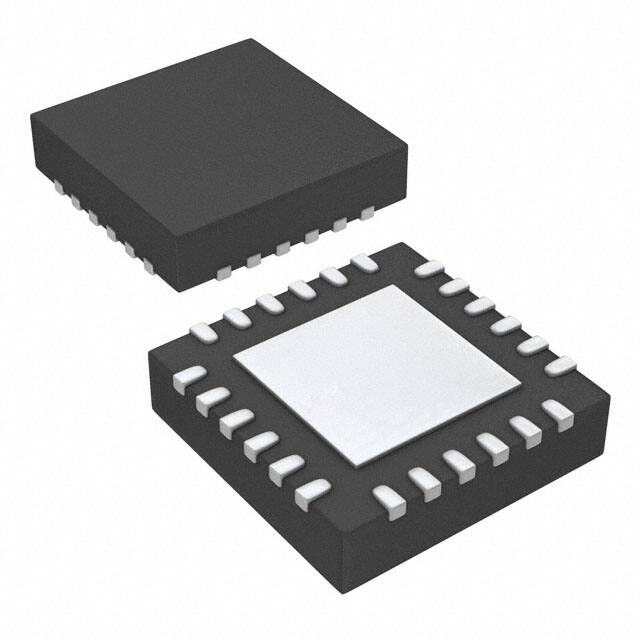


 工商网监
湘ICP备2023018690号
工商网监
湘ICP备2023018690号
