www.ti.com
Table of Contents
User’s Guide
TPS65261 Buck Converter Evaluation Module User's
Guide
ABSTRACT
This document presents the information required to operate the TPS65261 PMIC as well as the support
documentation including schematic, layout, hardware setup, and bill of materials (BOM).
Table of Contents
1 Background.............................................................................................................................................................................2
2 TPS65261 Schematic..............................................................................................................................................................3
3 Board Layout...........................................................................................................................................................................4
4 Bench Test Setup Conditions................................................................................................................................................ 6
5 Power-Up Procedure.............................................................................................................................................................. 8
6 Bill of Materials....................................................................................................................................................................... 9
7 Revision History................................................................................................................................................................... 10
List of Figures
Figure 2-1. TPS65261 Schematic................................................................................................................................................3
Figure 3-1. Component Placement (Top Layer)...........................................................................................................................4
Figure 3-2. Board Layout (Top Layer)..........................................................................................................................................5
Figure 3-3. Board Layout (Second Layer)................................................................................................................................... 5
Figure 3-4. Board Layout (Third Layer)....................................................................................................................................... 5
Figure 3-5. Board Layout (Bottom Layer).................................................................................................................................... 5
Figure 4-1. Header Descriptions and Jumper Placement............................................................................................................6
Trademarks
All trademarks are the property of their respective owners.
SLVUA85A – JUNE 2014 – REVISED MAY 2021
Submit Document Feedback
TPS65261 Buck Converter Evaluation Module User's Guide
Copyright © 2021 Texas Instruments Incorporated
1
�Background
www.ti.com
1 Background
The TPS65261 PMIC is a triple 3-A, 2-A, 2-A output current, synchronous step-down (buck) converter with an
operational range of 4.5 V to 18 V. The TPS65261 features an automatic power sequence with connecting
MODE pin to V7V and configuring EN1/2/3 pins. The device also features an open drain RESET signal to
monitor power down. The TPS65261 operates in pulse skipping mode (PSM) light load.
As there are many possible options to set the converters, Table 1-1 presents the performance specification
summary for the EVM.
Table 1-1. Summary of Performance
Test Conditions
Performance
VIN = 4.5 V to 18 V
fSW = 600 kHz
(25°C ambient)
BUCK1, 1.2 V, up to 3 A
BUCK2, 3.3 V, up to 2 A
BUCK3, 1.8 V, up to 2 A
RESET, pull low when VDIV lower than 1.23 V
This evaluation module is designed to provide access to the features of the TPS65261. Some modifications
can be made to this module to test performance at different input and output voltages, current and switching
frequency. Contact the TI Field Applications group for advice on these matters.
2
TPS65261 Buck Converter Evaluation Module User's Guide
Copyright © 2021 Texas Instruments Incorporated
SLVUA85A – JUNE 2014 – REVISED MAY 2021
Submit Document Feedback
�www.ti.com
TPS65261 Schematic
2 TPS65261 Schematic
Figure 2-1 shows the EVM schematic.
R1
C1
0.047µF
TP1
VOUT1 1.2V 3A
L1
0
TP2
VIN 12V
TP5
C7
10µF
J4
C8
10µF
C9
10µF
30
VDIV
V7V 5
C10
GND
1µF
TP9
V7V R9
100k
TP7
C2
22µF
4.7µH
28
12
13
29
VIN
1
2
3
GND
2
TP8
31
32
1
EN1
EN2
EN3
R11
100k
MODE
C17
C19
0.01µF
C20
0.01µF
4
U1
PVIN1
PVIN2
PVIN3
VIN
VDIV
26
COMP1
RESET
BST2
PGOOD
LX2
EN1
EN2
EN3
FB2
MODE
SS1
8
SS2
COMP2
20
73.2k
GND
21
20.0k
R8
9
3300pF
C11
0.047µF
6
GND
VFB2
16
LX3
15
R15
ROSC
COMP3
AGND
PGND1
PGND2
PGND3
19
C18
0.047µF
C5
DNI
82pF
27
11
14
22pF C24
R18
30k
VOUT2 3.3V 2A
TP6
C12
22µF
GND
C13
22µF
GND
1
2
R10
0
TP11
TP15
J2
C15
DNI
VFB2
R14
22pF
GND
R13
10.0k
45.3k
TP12
VOUT3 1.8V 2A
GND
C21
22µF
4.7µH
C23
GND
GND
L3
VFB3
VFB1
R5
10.0k
10.0k
GND
18
PAD
TPS65261RHB
GND
2200pF
0
SS3
J1
GND
22pF C16
R12
30k
TP3
R6
4.7µH
7
R2
0
L2
0
10
C3
22µF
TP4
22pF C6
R3
22 VFB1
23
BST3
FB3
R17
C4
C14
0.01µF
GND
LX1
FB1
V7V
24
17
BST1
25
1
2
GND
C22
22µF
GND
2200pF
R16
0
TP14
TP13
J3
C25
DNI
VFB3
R20
GND
2
1
22pF
GND
R19
10.0k
20.0k
GND
GND
GND
VIN
V7V
R4
147k
R21
100k
J5
R25
51k
C26
DNI
GND
R26
51k
EN1
R23
100k
J7
1
2
3
GND
GND
J6
1
2
3
VDIV
R7
20.0k
R22
100k
C27
DNI
R27
51k
GND
GND
EN2
GND
J8
1
2
3
1
2
3
TP10
GND
GND
GND
C28
DNI
EN3
MODE
Figure 2-1. TPS65261 Schematic
SLVUA85A – JUNE 2014 – REVISED MAY 2021
Submit Document Feedback
TPS65261 Buck Converter Evaluation Module User's Guide
Copyright © 2021 Texas Instruments Incorporated
3
�Board Layout
www.ti.com
3 Board Layout
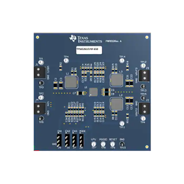
Figure 3-1 illustrates the PCB layout for this EVM.
Figure 3-1. Component Placement (Top Layer)
4
TPS65261 Buck Converter Evaluation Module User's Guide
Copyright © 2021 Texas Instruments Incorporated
SLVUA85A – JUNE 2014 – REVISED MAY 2021
Submit Document Feedback
�www.ti.com
Board Layout
3.1 EVM Layout
Figure 3-2 through Figure 3-5 illustrate the PCB layout for this EVM.
Figure 3-2. Board Layout (Top Layer)
Figure 3-3. Board Layout (Second Layer)
Figure 3-4. Board Layout (Third Layer)
Figure 3-5. Board Layout (Bottom Layer)
SLVUA85A – JUNE 2014 – REVISED MAY 2021
Submit Document Feedback
TPS65261 Buck Converter Evaluation Module User's Guide
Copyright © 2021 Texas Instruments Incorporated
5
�www.ti.com
Bench Test Setup Conditions
4 Bench Test Setup Conditions
4.1 Headers Description and Jumper Placement
Figure 4-1 illustrates the header description and jumper placement on the EVM.
Figure 4-1. Header Descriptions and Jumper Placement
Test points:
A: LX of VOUT1
B: LX of VOUT2
C: LX of VOUT3
VOUT1, VOUT2, VOUT3, VIN, PGOOD, RESET, V7V
6
TPS65261 Buck Converter Evaluation Module User's Guide
Copyright © 2021 Texas Instruments Incorporated
SLVUA85A – JUNE 2014 – REVISED MAY 2021
Submit Document Feedback
�www.ti.com
Bench Test Setup Conditions
Table 4-1 lists the I/O connections.
Table 4-1. Input/Output Connection
Number
Function
J1
BUCK1 connector
Description
Output of BUCK1
J2
BUCK2 connector
Output of BUCK2
J3
BUCK3 connector
Output of BUCK3
J4
VIN connector
Apply power supply to this connector
4.2 Jumpers and Switches
Table 4-2 lists the jumpers on the EVM.
Table 4-2. Jumpers
Jumper
Function
Placement
J5
Buck1 enable (EN1)
Connect EN1 to GND to disable VOUT1, connect EN1 to VIN through a 100-kΩ resistor to
enable VOUT1; leave open to enable VOUT1
J6
Buck2 enable (EN2)
Connect EN2 to GND to disable VOUT2, connect EN2 to VIN through a 100-kΩ resistor to
enable VOUT2; leave open to enable VOUT2
J7
Buck3 enable (EN3)
Connect EN3 to GND to disable VOUT3, connect EN3 to VIN through a 100-kΩ resistor to
enable VOUT3; leave open to enable VOUT3
J8
Mode
Power sequencing mode control pin. Connect this pin to GND to set power sequence with
dedicated enable pin; connect this pin to V7V, set the power sequence with the pre-defined
power up and power down sequence.
SLVUA85A – JUNE 2014 – REVISED MAY 2021
Submit Document Feedback
TPS65261 Buck Converter Evaluation Module User's Guide
Copyright © 2021 Texas Instruments Incorporated
7
�Power-Up Procedure
www.ti.com
5 Power-Up Procedure
Power sequence with dedicated enable pin:
1.
2.
3.
4.
Connect J8 to GND
Apply 4.5 V - 18 V to J4
Toggle J5, J6, or J7 to enable VOUT1, VOUT2, and VOUT3, respectively
Apply loads to the output connectors
Power sequence with the pre-defined power up and power down sequence:
1.
2.
3.
4.
5.
8
Connect J8 to V7V
Connect J5 to High (or Low), J6 to High (or Low)
Apply 4.5 V - 18 V to J4
Toggle J7 to enable VOUT1, VOUT2, and VOUT3
Apply loads to the output connectors.
TPS65261 Buck Converter Evaluation Module User's Guide
Copyright © 2021 Texas Instruments Incorporated
SLVUA85A – JUNE 2014 – REVISED MAY 2021
Submit Document Feedback
�www.ti.com
Bill of Materials
6 Bill of Materials
Table 6-1 lists the BOM for this EVM.
Table 6-1. TPS65261 Bill of Materials
Designator
Qty
Value
Description
!PCB1
1
Package Reference
Part Number
Manufacturer
PWR650
C1, C11, C18
3
0.047uF
CAP, CERM, 0.047uF, 50V, +/-10%, X7R, 0603
Any
0603
C1608X7R1H473K
C2, C3, C12, C13, C21,
C22
6
22uF
TDK
CAP, CERM, 22uF, 16V, +/-20%, X5R, 1206
1206
1206YD226MAT2A
AVX
C4, C14, C15, C23, C25
5
C5
1
22pF
CAP, CERM, 22pF, 50V, +/-5%, C0G/NP0, 0603
0603
06035A220JAT2A
AVX
82pF
CAP, CERM, 82pF, 50V, +/-5%, C0G/NP0, 0603
0603
06035A820JAT2A
C6
AVX
1
3300pF
CAP, CERM, 3300pF, 50V, +/-10%, X7R, 0603
0603
C0603C332K5RACTU
Kemet
C7, C8, C9
3
10uF
CAP, CERM, 10uF, 25V, +/-10%, X5R, 1206
1206
GRM31CR61E106KA12L
MuRata
C10
1
1uF
CAP, CERM, 1uF, 25V, +/-10%, X7R, 0603
0603
C1608X7R1E105K080AB
TDK
C16, C24
2
2200pF
CAP, CERM, 2200pF, 50V, +/-10%, X7R, 0603
0603
C0603C222K5RACTU
Kemet
C17, C19, C20
3
0.01uF
CAP, CERM, 0.01uF, 50V, +/-5%, X7R, 0603
0603
C0603C103J5RACTU
Kemet
C26, C27, C28
0
DNI
CAP, CERM, 0.01uF, 50V, +/-5%, X7R, 0603
0603
C0603C103J5RACTU
Kemet
J1, J2, J3, J4
4
Terminal Block, 6A, 3.5mm Pitch, 2-Pos, TH
7.0x8.2x6.5mm
ED555/2DS
On-Shore Technology
J5, J6, J7, J8
4
Header, 100mil, 3x1, Tin plated, TH
Header, 3 PIN, 100mil, Tin
PEC03SAAN
Sullins Connector Solutions
L1, L2, L3
3
Inductor, Shielded Drum Core, Superflux, 4.7uH, 6A, 0.02 ohm, SMD
WE-HC4
744311470
Wurth Elektronik eiSos
LBL1
1
Thermal Transfer Printable Labels, 0.650" W x 0.200" H - 10,000 per roll
PCB Label 0.650"H x 0.200"W
THT-14-423-10
Brady
Printed Circuit Board
4.7uH
R1, R2, R8, R10, R15, R16 6
0
RES, 0 ohm, 5%, 0.1W, 0603
0603
CRCW06030000Z0EA
Vishay-Dale
R3, R7, R20
3
20.0k
RES, 20.0k ohm, 1%, 0.1W, 0603
0603
CRCW060320K0FKEA
Vishay-Dale
R4
1
147k
RES, 147k ohm, 1%, 0.1W, 0603
0603
CRCW0603147KFKEA
Vishay-Dale
R5, R6, R13, R19
4
10.0k
RES, 10.0k ohm, 1%, 0.1W, 0603
0603
CRCW060310K0FKEA
Vishay-Dale
R9, R11, R21, R22, R23
5
100k
RES, 100k ohm, 1%, 0.1W, 0603
0603
CRCW0603100KFKEA
Vishay-Dale
R12, R18
2
30k
RES, 30k ohm, 5%, 0.1W, 0603
0603
CRCW060330K0JNEA
Vishay-Dale
R14
1
45.3k
RES, 45.3k ohm, 1%, 0.1W, 0603
0603
CRCW060345K3FKEA
Vishay-Dale
R17
1
73.2k
RES, 73.2k ohm, 1%, 0.1W, 0603
0603
CRCW060373K2FKEA
Vishay-Dale
R25, R26, R27
3
51k
RES, 51k ohm, 5%, 0.1W, 0603
0603
CRCW060351K0JNEA
Vishay-Dale
SH-J1
1
1x2
Shunt, 100mil, Gold plated, Black
Shunt
969102-0000-DA
3M
TP1, TP2, TP6, TP7, TP8,
TP9, TP12
7
White
Test Point, Miniature, White, TH
White Miniature Testpoint
5002
Keystone
TP3, TP5, TP10, TP13,
TP15
5
Black
Test Point, Miniature, Black, TH
Black Miniature Testpoint
5001
Keystone
TP4, TP11, TP14
0
DNI
Test Point, Miniature, White, TH
White Miniature Testpoint
5002
Keystone
U1
1
4.5V to 18V Input Voltage, 3A/2A/2A Output Current Triple Synchronous StepDown Converter, RHB0032E
RHB0032E
TPS65261RHB
Texas Instruments
Note:
Unless otherwise noted in the columns, all parts may be substituted with equivalents.
SLVUA85A – JUNE 2014 – REVISED MAY 2021
Submit Document Feedback
TPS65261 Buck Converter Evaluation Module User's Guide
Copyright © 2021 Texas Instruments Incorporated
9
�Revision History
www.ti.com
7 Revision History
NOTE: Page numbers for previous revisions may differ from page numbers in the current version.
Changes from Revision * (June 2014) to Revision A (May 2021)
Page
• Updated user's guide title................................................................................................................................... 2
• Updated the numbering format for tables, figures, and cross-references throughout the document. ................2
10
TPS65261 Buck Converter Evaluation Module User's Guide
Copyright © 2021 Texas Instruments Incorporated
SLVUA85A – JUNE 2014 – REVISED MAY 2021
Submit Document Feedback
�IMPORTANT NOTICE AND DISCLAIMER
TI PROVIDES TECHNICAL AND RELIABILITY DATA (INCLUDING DATA SHEETS), DESIGN RESOURCES (INCLUDING REFERENCE
DESIGNS), APPLICATION OR OTHER DESIGN ADVICE, WEB TOOLS, SAFETY INFORMATION, AND OTHER RESOURCES “AS IS”
AND WITH ALL FAULTS, AND DISCLAIMS ALL WARRANTIES, EXPRESS AND IMPLIED, INCLUDING WITHOUT LIMITATION ANY
IMPLIED WARRANTIES OF MERCHANTABILITY, FITNESS FOR A PARTICULAR PURPOSE OR NON-INFRINGEMENT OF THIRD
PARTY INTELLECTUAL PROPERTY RIGHTS.
These resources are intended for skilled developers designing with TI products. You are solely responsible for (1) selecting the appropriate
TI products for your application, (2) designing, validating and testing your application, and (3) ensuring your application meets applicable
standards, and any other safety, security, regulatory or other requirements.
These resources are subject to change without notice. TI grants you permission to use these resources only for development of an
application that uses the TI products described in the resource. Other reproduction and display of these resources is prohibited. No license
is granted to any other TI intellectual property right or to any third party intellectual property right. TI disclaims responsibility for, and you
will fully indemnify TI and its representatives against, any claims, damages, costs, losses, and liabilities arising out of your use of these
resources.
TI’s products are provided subject to TI’s Terms of Sale or other applicable terms available either on ti.com or provided in conjunction with
such TI products. TI’s provision of these resources does not expand or otherwise alter TI’s applicable warranties or warranty disclaimers for
TI products.
TI objects to and rejects any additional or different terms you may have proposed. IMPORTANT NOTICE
Mailing Address: Texas Instruments, Post Office Box 655303, Dallas, Texas 75265
Copyright © 2022, Texas Instruments Incorporated
�


 工商网监
湘ICP备2023018690号
工商网监
湘ICP备2023018690号
