Product
Folder
Sample &
Buy
Support &
Community
Tools &
Software
Technical
Documents
TPS65263
SLVSCN0A – JUNE 2014 – REVISED SEPTEMBER 2014
TPS65263, 4.5- to 18-V Input Voltage, 3-A/2-A/2-A Output Current Triple Synchronous
Step-Down Converter With I2C Controlled Dynamic Voltage Scaling
1 Features
3 Description
•
The TPS65263 incorporates triple synchronous buck
converters with 4.5- to 18-V wide input voltage range
that encompassed most intermediate bus voltage
operating off 5-, 9-, 12-, or 15-V power bus or battery.
The converter, with constant frequency peak current
mode, is designed to simplify its application while
giving designers options to optimize the system
according to targeted applications. The device
operates in 600 kHz with 180° out-of-phase between
buck1 and buck2, buck3 (buck2 and buck3 run in
phase).
1
•
•
•
•
•
•
•
•
•
Operating Input Voltage Range 4.5- to 18-V
Continuous Output Current 3 A/2 A/2 A
I2C Controlled 7-Bits VID Programmable Output
Voltage from 0.68 to 1.95 V With 10-mV Voltage
Step for Each Buck
I2C Controlled VID Voltage Transition Slew Rate
I2C Read Back Power Good Status, Overcurrent
Warning for Each Buck
I2C Read Back Die Temperature Warning
I2C Compatible Interface With Standard Mode
(100 kHz) and Fast Mode (400 kHz)
Feedback Reference Voltage 0.6 V ±1%
Fixed 600-kHz Frequency
Dedicated Enable and Soft Start Pins for Each
Buck
Thermal Overloading Protection
2 Applications
•
•
•
•
DTV LCD Panel
Set-Top Boxes
Home Gateway and Access Point Networks
Surveillance
The initial startup voltage of each buck can be set
with external feedback resistors. The output voltage
of each buck can be dynamically scaled from 0.68 to
1.95 V in 10-mV step with I2C controlled 7 bits VID.
The VID voltage transition slew rate is programmable
with 3-bits control through I2C bus to optimize
overshoot/undershoot during VID voltage transition.
Each buck in TPS65263 can be I2C controlled for
enabling/disabling output voltage, setting the pulse
skipping mode (PSM) or force continuous current
mode (FCC) at light load condition and reading the
power good status, overcurrent warning and die
temperature warning.
The TPS65263 features overvoltage, overcurrent,
short-circuit, and overtemperature protection.
Device Information(1)
PART NUMBER
TPS65263
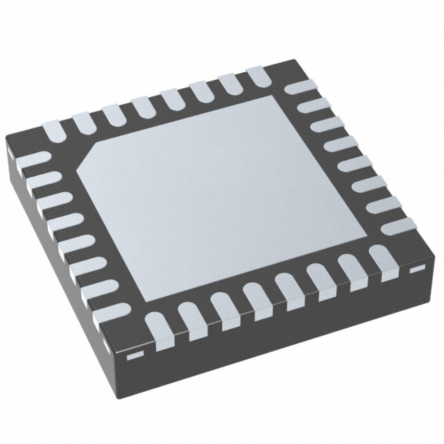
PACKAGE
VQFN (32)
BODY SIZE (NOM)
5.00 mm × 5.00 mm
(1) For all available packages, see the orderable addendum at
the end of the data sheet.
Efficiency vs Output Load
4 Typical Application
100%
Vout1
Vin
PVINx
VIN
90%
LX1
80%
TPS65263
70%
Vout1
Vout2
Vout3
DVCC
VOUT1
Vout2
VOUT2
LX2
VOUT3
ENx
SSx
FB2
SCL
60%
50%
40%
30%
Vout3
SDA
Efficiency (%)
FB1
LX3
20%
SDA
10%
SCL
AGND
FB3
PGND
0%
0.01
0.10
Output Load (A)
A.
1.00
C001
VIN = 12 V; VOUT = 3.3 V
1
An IMPORTANT NOTICE at the end of this data sheet addresses availability, warranty, changes, use in safety-critical applications,
intellectual property matters and other important disclaimers. PRODUCTION DATA.
�TPS65263
SLVSCN0A – JUNE 2014 – REVISED SEPTEMBER 2014
www.ti.com
Table of Contents
1
2
3
4
5
6
7
8
9
Features ..................................................................
Applications ...........................................................
Description .............................................................
Typical Application ................................................
Revision History.....................................................
Device Comparison Table.....................................
Pin Configuration and Functions .........................
Specifications.........................................................
1
1
1
1
2
3
3
5
8.1
8.2
8.3
8.4
8.5
8.6
5
5
5
5
6
8
Absolute Maximum Ratings ......................................
Handling Ratings ......................................................
Recommended Operating Conditions.......................
Thermal Information ..................................................
Electrical Characteristics...........................................
Typical Characteristics ..............................................
Detailed Description ............................................ 12
9.1 Overview ................................................................. 12
9.2
9.3
9.4
9.5
Functional Block Diagram .......................................
Feature Description.................................................
Device Functional Modes........................................
Register Maps .........................................................
13
14
22
24
10 Application and Implementation........................ 28
10.1 Application Information.......................................... 28
10.2 Typical Application ............................................... 28
11 Power Supply Recommendations ..................... 36
12 Layout................................................................... 36
12.1 Layout Guidelines ................................................. 36
12.2 Layout Example .................................................... 37
13 Device and Documentation Support ................. 38
13.1 Trademarks ........................................................... 38
13.2 Electrostatic Discharge Caution ............................ 38
13.3 Glossary ................................................................ 38
14 Mechanical, Packaging, and Orderable
Information ........................................................... 38
5 Revision History
Changes from Original (June 2014) to Revision A
•
2
Page
Updated device from product preview to production data ..................................................................................................... 1
Submit Documentation Feedback
Copyright © 2014, Texas Instruments Incorporated
Product Folder Links: TPS65263
�TPS65263
www.ti.com
SLVSCN0A – JUNE 2014 – REVISED SEPTEMBER 2014
6 Device Comparison Table
PART
NUMBER
DESCRIPTION
COMMENTS
TPS65261/-1
4.5 to 18 V, triple bucks with input
voltage power failure indicator
Triple bucks 3-A/2-A/2-A output current, features an open drain RESET signal to
monitor input power failure, automatic power sequencing
TPS65262/-1
4.5 to 18 V, triple bucks with dual
adjustable LDOs
Triple bucks 3-A/1-A/1-A output current, automatic power sequencing. dual LDOs:
TPS65262, 200 mA/100 mA; TPS65262-1, 350 mA/150 mA
TPS65287
4.5 to 18 V, triple bucks with
power switch and push button
control
Triple bucks 3-A/2-A/2-A output current, up to 2.1-A USB power with over current
setting by external resistor, push button control for intelligent system power-on/poweroff operation
TPS65288
4.5 to 18 V, triple bucks with dual
power switches
Triple bucks 3-A/2-A/2-A output current, 2 USB power switches current limiting at
typical 1.2 A (0.8, 1.0, 1.4, 1.6, 1.8, 2.0, 2.2 A available with manufacture trim options)
7 Pin Configuration and Functions
16
15
14
17 SS3
18 COMP3
19 FB3
20 VOUT3
21 VOUT1
22 FB1
23 COMP1
LX3
PGND3
13
PVIN1
25
PGND1
26
LX1
BST3
PVIN3
28
BST1
27
24 SS1
RHB Package
32 Pin
Top View
29
12
11
10
LX2
9
BST2
1
2
3
4
5
6
7
8
EN3
SDA
SCL
AGND
VOUT2
FB2
COMP2
SS2
EN2
30
EN1
PGND2
32
V7V
PVIN2
31
Thermal Pad
VIN
(There is no electric signal down bonded to thermal pad inside IC.
Exposed thermal pad must be soldered to PCB for optimal thermal performance.)
Pin Functions
PIN
NAME
DESCRIPTION
NO.
EN3
1
Enable for buck3. Float to enable. Can use this pin to adjust the input undervoltage lockout (UVLO) of buck3 with a
resistor divider.
SDA
2
I2C interface data pin
SCL
3
I2C interface clock pin
AGND
4
Analog ground common to buck controllers and other analog circuits. It must be routed separately from high current
power grounds to the (–) terminal of bypass capacitor of input voltage VIN.
Submit Documentation Feedback
Copyright © 2014, Texas Instruments Incorporated
Product Folder Links: TPS65263
3
�TPS65263
SLVSCN0A – JUNE 2014 – REVISED SEPTEMBER 2014
www.ti.com
Pin Functions (continued)
PIN
NAME
DESCRIPTION
NO.
VOUT2
5
Buck2 output voltage sense pin.
FB2
6
Feedback Kelvin sensing pin for buck2 output voltage. Connect this pin to buck2 resistor divider.
COMP2
7
Error amplifier output and Loop compensation pin for buck2. Connect a series resistor and capacitor to compensate the
control loop of buck2 with peak current PWM mode.
SS2
8
Soft-start and tracking input for buck2. An internal 5uA pullup current source is connected to this pin. The soft-start time
can be programmed by connecting a capacitor between this pin and ground.
BST2
9
Boot strapped supply to the high side floating gate driver in buck2. Connect a capacitor (recommend 47nF) from BST2
pin to LX2 pin.
LX2
10
Switching node connection to the inductor and bootstrap capacitor for buck2. The voltage swing at this pin is from a
diode voltage below the ground up to PVIN2 voltage.
PGND2
11
Power ground connection of buck2. Connect PGND2 pin as close as practical to the (–) terminal of PVIN2 input ceramic
capacitor.
PVIN2
12
Input power supply for buck2. Connect PVIN2 pin as close as practical to the (+) terminal of an input ceramic capacitor
(suggest 10 µF).
PVIN3
13
Input power supply for buck3. Connect PVIN3 pin as close as practical to the (+) terminal of an input ceramic capacitor
(suggest 10 µF).
PGND3
14
Power ground connection of buck3. Connect PGND3 pin as close as practical to the (–) terminal of PVIN3 input ceramic
capacitor.
LX3
15
Switching node connection to the inductor and bootstrap capacitor for buck3. The voltage swing at this pin is from a
diode voltage below the ground up to PVIN3 voltage.
BST3
16
Boot strapped supply to the high side floating gate driver in buck3. Connect a capacitor (recommend 47 nF) from BST3
pin to LX3 pin.
SS3
17
Soft-start and tracking input for buck3. An internal 5-µA pullup current source is connected to this pin. The soft-start time
can be programmed by connecting a capacitor between this pin and ground.
COMP3
18
Error amplifier output and Loop compensation pin for buck3. Connect a series resistor and capacitor to compensate the
control loop of buck3 with peak current PWM mode.
FB3
19
Feedback Kelvin sensing pin for buck3 output voltage. Connect this pin to buck3 resistor divider.
VOUT3
20
Buck3 output voltage sense pin.
VOUT1
21
Buck1 output voltage sense pin.
FB1
22
Feedback Kelvin sensing pin for buck1 output voltage. Connect this pin to buck1 resistor divider.
COMP1
23
Error amplifier output and Loop compensation pin for buck1. Connect a series resistor and capacitor to compensate the
control loop of buck1 with peak current PWM mode.
SS1
24
Soft-start and tracking input for buck1. An internal 5-µA pullup current source is connected to this pin. The soft-start time
can be programmed by connecting a capacitor between this pin and ground.
BST1
25
Boot strapped supply to the high side floating gate driver in buck1. Connect a capacitor (recommend 47 nF) from BST1
pin to LX1 pin.
LX1
26
Switching node connection to the inductor and bootstrap capacitor for buck1. The voltage swing at this pin is from a
diode voltage below the ground up to PVIN1 voltage.
PGND1
27
Power ground connection of Buck1. Connect PGND1 pin as close as practical to the (–) terminal of PVIN1 input ceramic
capacitor.
PVIN1
28
Input power supply for buck1. Connect PVIN1 pin as close as practical to the (+) terminal of an input ceramic capacitor
(suggest 10 µF).
VIN
29
Buck controller power supply.
V7V
30
Internal LDO for gate driver and internal controller. Connect a 1-µF capacitor from the pin to power ground.
EN1
31
Enable for buck1. Float to enable. Can use this pin to adjust the input UVLO of buck1 with a resistor divider.
EN2
32
Enable for buck2. Float to enable. Can use this pin to adjust the input UVLO of buck2 with a resistor divider.
PAD
—
There is no electric signal down bonded to thermal pad inside IC. Exposed thermal pad must be soldered to PCB for
optimal thermal performance.
4
Submit Documentation Feedback
Copyright © 2014, Texas Instruments Incorporated
Product Folder Links: TPS65263
�TPS65263
www.ti.com
SLVSCN0A – JUNE 2014 – REVISED SEPTEMBER 2014
8 Specifications
8.1 Absolute Maximum Ratings
over operating free-air temperature (unless otherwise noted)
Voltage
TJ
(1)
(1)
MIN
MAX
PVIN1, PVIN2, PVIN3,VIN
–0.3
20
LX1, LX2, LX3 (maximum withstand voltage transient
www.ti.com
1
1
´
V
8 ´ ƒ sw
oripple
Ioripple
(12)
Equation 13 calculates the maximum ESR an output capacitor can have to meet the output voltage ripple
specification.
Voripple
Re sr <
Ioripple
(13)
Additional capacitance de-ratings for aging, temperature and DC bias should be factored in which increases this
minimum value. Capacitors generally have limits to the amount of ripple current they can handle without failing or
producing excess heat. An output capacitor that can support the inductor ripple current must be specified. Some
capacitor data sheets specify the root mean square (RMS) value of the maximum ripple current. Equation 14 can
be used to calculate the RMS ripple current the output capacitor needs to support.
Icorms =
Vout ´ (Vinmax - Vout )
12 ´ Vinmax ´ L ´ ƒ sw
(14)
10.2.2.3 Input Capacitor Selection
The TPS65263 requires a high quality ceramic, type X5R or X7R, input decoupling capacitor of at least 10 µF of
effective capacitance on the PVIN input voltage pins. In some applications additional bulk capacitance may also
be required for the PVIN input. The effective capacitance includes any DC bias effects. The voltage rating of the
input capacitor must be greater than the maximum input voltage. The capacitor must also have a ripple current
rating greater than the maximum input current ripple of The TPS65263. The input ripple current can be calculated
using Equation 15.
Iinrms = Iout ´
(Vinmin - Vout )
Vout
´
Vinmin
Vinmin
(15)
The value of a ceramic capacitor varies significantly over temperature and the amount of DC bias applied to the
capacitor. The capacitance variations due to temperature can be minimized by selecting a dielectric material that
is stable over temperature. X5R and X7R ceramic dielectrics are usually selected for power regulator capacitors
because they have a high capacitance to volume ratio and are fairly stable over temperature. The output
capacitor must also be selected with the DC bias taken into account. The capacitance value of a capacitor
decreases as the DC bias across a capacitor increases. The input capacitance value determines the input ripple
voltage of the regulator. The input voltage ripple can be calculated using Equation 16.
I
´ 0.25
DVin = out max
Cin ´ ƒ sw
(16)
10.2.2.4 Loop Compensation
The TPS65263 incorporates a peak current mode control scheme. The error amplifier is a trans-conductance
amplifier with a gain of 300 µS. A typical type II compensation circuit adequately delivers a phase margin
between 60° and 90°. Cb adds a high frequency pole to attenuate high frequency noise when needed. To
calculate the external compensation components, follow the following steps.
1. Select switching frequency ƒSW that is appropriate for application depending on L and C sizes, output ripple,
EMI, and etc. Switching frequency between 500 kHz to 1 MHz gives best trade-off between performance and
cost. To optimize efficiency, lower switching frequency is desired.
2. Set up cross over frequency, ƒc, which is typically between 1/5 and 1/20 of ƒSW.
3. RC can be determined by
2p ´ ƒc ´ Vo ´ Co
RC =
Gm-EA ´ Vref ´ Gm-PS
(17)
æ
ö
1
ç ƒp =
÷.
Co ´ RL ´ 2p ø
4. Calculate CC by placing a compensation zero at or before the dominant pole è
30
Submit Documentation Feedback
Copyright © 2014, Texas Instruments Incorporated
Product Folder Links: TPS65263
�TPS65263
www.ti.com
CC =
SLVSCN0A – JUNE 2014 – REVISED SEPTEMBER 2014
RL ´ Co
RC
(18)
5. Optional Cb can be used to cancel the zero from the ESR associated with CO.
R
´ Co
Cb = ESR
RC
LX
VOUT
iL
Current Sense
I/V Converter
RESR
RL
Gm_PS = 7.4 A/V
Co
R1
Vfb
COMP
(19)
C1
FB
EA
Vref = 0.6 V
R2
Rc
Cb
Gm_EA = 300 uS
Cc
Figure 41. DC/DC Loop Compensation
Submit Documentation Feedback
Copyright © 2014, Texas Instruments Incorporated
Product Folder Links: TPS65263
31
�TPS65263
SLVSCN0A – JUNE 2014 – REVISED SEPTEMBER 2014
www.ti.com
10.2.3 Application Curves
32
Figure 42. BUCK1, Soft-Start, Iout = 3 A
Figure 43. BUCK2, Soft-Start, Iout = 2 A
Figure 44. BUCK3, Soft-Start, Iout = 2 A
Figure 45. BUCK1, Output Voltage Ripple, Iout = 3 A
Figure 46. BUCK2, Output Voltage Ripple, Iout = 3 A
Figure 47. BUCK3, Output Voltage Ripple, Iout = 2 A
Submit Documentation Feedback
Copyright © 2014, Texas Instruments Incorporated
Product Folder Links: TPS65263
�TPS65263
www.ti.com
SLVSCN0A – JUNE 2014 – REVISED SEPTEMBER 2014
Figure 48. BUCK1, Load Transient, 0.75 to 1.5 A
SR = 0.25 A/µs
Figure 49. BUCK1, Load Transient, 1.5 to 2.25 A
SR = 0.25 A/µs
Figure 50. BUCK2, Load Transient, 0.5 to 1 A
SR = 0.25 A/µs
Figure 51. BUCK2, Load Transient, 1 to 1.5 A
SR = 0.25 A/µs
Figure 52. BUCK3, Load Transient, 0.5 to 1 A
SR = 0.25 A/µs
Figure 53. BUCK3, Load Transient, 1 to 1.5 A
SR = 0.25 A/µs
Submit Documentation Feedback
Copyright © 2014, Texas Instruments Incorporated
Product Folder Links: TPS65263
33
�TPS65263
SLVSCN0A – JUNE 2014 – REVISED SEPTEMBER 2014
34
www.ti.com
Figure 54. BUCK1, Hiccup and Recovery
Figure 55. BUCK2, Hiccup and Recovery
Figure 56. BUCK3, Hiccup and Recovery
Figure 57. 180° Out-of-Phase
Figure 58. VID1 from 00 to 7F, SR = 10 mV/cycle
Figure 59. VID1 from 7F to 00, SR = 10 mV/cycle
Submit Documentation Feedback
Copyright © 2014, Texas Instruments Incorporated
Product Folder Links: TPS65263
�TPS65263
www.ti.com
SLVSCN0A – JUNE 2014 – REVISED SEPTEMBER 2014
Figure 60. VID2 from 00 to 7F, SR = 10 mV/cycle
Figure 61. VID2 from 7F to 00, SR = 10 mV/cycle
Figure 62. VID3 from 00 to 7F, SR = 10 mV/cycle
Figure 63. VID3 from 7F to 00, SR = 10 mV/cycle
VIN = 12 V; VOUT1 = 1.5 V / 1.5 A; VOUT2 = 1.2 V / 1 A
VOUT3 = 2.5 V / 1 A
TA = 26.8°C
VIN = 12 V; VOUT1 = 1.5 V / 3 A; VOUT2 = 1.2 V / 2 A
VOUT3 = 2.5 V / 2 A
TA = 26.8°C
Figure 64. Thermal Signature of TPS65263EVM, 4-Layer
EVM Condition, 75 mm × 75 mm
Figure 65. Thermal Signature of TPS65263EVM, 4-Layer
EVM Condition, 75 mm × 75 mm
Submit Documentation Feedback
Copyright © 2014, Texas Instruments Incorporated
Product Folder Links: TPS65263
35
�TPS65263
SLVSCN0A – JUNE 2014 – REVISED SEPTEMBER 2014
www.ti.com
11 Power Supply Recommendations
The devices are designed to operate from an input voltage supply range between 4.5 to 18 V. This input power
supply should be well regulated. If the input supply is located more than a few inches from the TPS65263
converter additional bulk capacitance may be required in addition to the ceramic bypass capacitors. An
electrolytic capacitor with a value of 47 μF is a typical choice.
12 Layout
12.1 Layout Guidelines
The TPS65263 can be layout on 2-layer PCB, shown in Figure 66.
Layout is a critical portion of good power supply design. See Figure 66 for a PCB layout example. The top
contains the main power traces for PVIN, VOUT, and LX. Also on the top layer are connections for the remaining
pins of the TPS65263 and a large top side area filled with ground. The top layer ground area should be
connected to the bottom layer ground using vias at the input bypass capacitor, the output filter capacitor and
directly under the TPS65263 device to provide a thermal path from the exposed thermal pad land to ground. The
bottom layer acts as ground plane connecting analog ground and power ground.
For operation at full rated load, the top side ground area together with the bottom side ground plane must provide
adequate heat dissipating area. There are several signals paths that conduct fast changing currents or voltages
that can interact with stray inductance or parasitic capacitance to generate noise or degrade the power supplies
performance. To help eliminate these problems, the PVIN pin should be bypassed to ground with a low ESR
ceramic bypass capacitor with X5R or X7R dielectric. Care should be taken to minimize the loop area formed by
the bypass capacitor connections, the PVIN pins, and the ground connections. The VIN pin must also be
bypassed to ground using a low ESR ceramic capacitor with X5R or X7R dielectric.
Since the LX connection is the switching node, the output inductor should be located close to the LX pins, and
the area of the PCB conductor minimized to prevent excessive capacitive coupling. The output filter capacitor
ground should use the same power ground trace as the PVIN input bypass capacitor. Try to minimize this
conductor length while maintaining adequate width. The small signal components should be grounded to the
analog ground path.
The FB and COMP pins are sensitive to noise so the resistors and capacitors should be located as close as
possible to the IC and routed with minimal lengths of trace. The additional external components can be placed
approximately as shown.
36
Submit Documentation Feedback
Copyright © 2014, Texas Instruments Incorporated
Product Folder Links: TPS65263
�TPS65263
www.ti.com
SLVSCN0A – JUNE 2014 – REVISED SEPTEMBER 2014
12.2 Layout Example
VOUT1
SS3
COMP3
VOUT3
FB3
FB1
VOUT1
SS1
COMP1
VOUT3
BST3
BST1
PGND3
PVIN1
PVIN3
COMP2
BST2
PVIN
SS2
LX2
EN2
FB2
EN1
VOUT
PGND2
SCL
PVIN2
V7V
AGND
VIN
EN3
VIN
LX3
PGND1
SDA
PVIN
LX1
VOUT2
TOPSIDE
GROUND
AREA
0.010 in. Diameter
Thermal VIA to Ground Plane
VIA to Ground Plane
Figure 66. PCB Layout
Submit Documentation Feedback
Copyright © 2014, Texas Instruments Incorporated
Product Folder Links: TPS65263
37
�TPS65263
SLVSCN0A – JUNE 2014 – REVISED SEPTEMBER 2014
www.ti.com
13 Device and Documentation Support
13.1 Trademarks
NXP is a trademark of NXP Semiconductors.
13.2 Electrostatic Discharge Caution
These devices have limited built-in ESD protection. The leads should be shorted together or the device placed in conductive foam
during storage or handling to prevent electrostatic damage to the MOS gates.
13.3 Glossary
SLYZ022 — TI Glossary.
This glossary lists and explains terms, acronyms, and definitions.
14 Mechanical, Packaging, and Orderable Information
The following pages include mechanical, packaging, and orderable information. This information is the most
current data available for the designated devices. This data is subject to change without notice and revision of
this document. For browser-based versions of this data sheet, refer to the left-hand navigation.
38
Submit Documentation Feedback
Copyright © 2014, Texas Instruments Incorporated
Product Folder Links: TPS65263
�PACKAGE OPTION ADDENDUM
www.ti.com
10-Dec-2020
PACKAGING INFORMATION
Orderable Device
Status
(1)
Package Type Package Pins Package
Drawing
Qty
Eco Plan
(2)
Lead finish/
Ball material
MSL Peak Temp
Op Temp (°C)
Device Marking
(3)
(4/5)
(6)
TPS65263RHBR
ACTIVE
VQFN
RHB
32
3000
RoHS & Green
NIPDAU
Level-2-260C-1 YEAR
TPS65263RHBT
ACTIVE
VQFN
RHB
32
250
RoHS & Green
NIPDAU
Level-2-260C-1 YEAR
-40 to 85
TPS
65263
TPS
65263
(1)
The marketing status values are defined as follows:
ACTIVE: Product device recommended for new designs.
LIFEBUY: TI has announced that the device will be discontinued, and a lifetime-buy period is in effect.
NRND: Not recommended for new designs. Device is in production to support existing customers, but TI does not recommend using this part in a new design.
PREVIEW: Device has been announced but is not in production. Samples may or may not be available.
OBSOLETE: TI has discontinued the production of the device.
(2)
RoHS: TI defines "RoHS" to mean semiconductor products that are compliant with the current EU RoHS requirements for all 10 RoHS substances, including the requirement that RoHS substance
do not exceed 0.1% by weight in homogeneous materials. Where designed to be soldered at high temperatures, "RoHS" products are suitable for use in specified lead-free processes. TI may
reference these types of products as "Pb-Free".
RoHS Exempt: TI defines "RoHS Exempt" to mean products that contain lead but are compliant with EU RoHS pursuant to a specific EU RoHS exemption.
Green: TI defines "Green" to mean the content of Chlorine (Cl) and Bromine (Br) based flame retardants meet JS709B low halogen requirements of


 工商网监
湘ICP备2023018690号
工商网监
湘ICP备2023018690号

