Sample &
Buy
Product
Folder
Support &
Community
Tools &
Software
Technical
Documents
TPS65631W
SLVSC27D – JULY 2013 – REVISED OCTOBER 2016
TPS65631W Dual-Output AMOLED Display Power Supply
1 Features
3 Description
•
•
•
•
•
The TPS65631W is designed to drive AMOLED
(Active Matrix Organic Light Emitting Diode) displays
requiring positive and negative supply rails. The
device integrates a boost converter for VPOS and an
inverting buck boost converter for VNEG and is
suitable for battery-operated products. The digital
control pin (CTRL) allows programming the negative
output voltage in digital steps. The TPS65631W uses
a novel technology enabling excellent line transient
performance.
1
•
•
•
•
•
•
2.9-V to 4.5-V Input Voltage Range
Fixed 4.6-V Positive Output Voltage
0.5% VPOS Accuracy from 25ºC to 85ºC
Separate VPOS Output Sense Pin
Negative Output Voltage Digitally Programmable
from –1.4 V to –4.4 V (–4 V Default)
Output Currents up to 200 mA Supported
Excellent Line Transient Regulation
Outputs High Impedance During Shut Down
Short-Circuit Protection
Thermal Shutdown
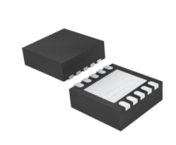
Available in 2.5-mm × 2.5-mm, 10-Pin QFN
Package
Device Information(1)
PART NUMBER
TPS65631W
PACKAGE
QFN (10)
BODY SIZE (NOM)
2.50 mm × 2.50 mm
(1) For all available packages, see the orderable addendum at
the end of the data sheet
spacer
2 Applications
spacer
AMOLED Displays
spacer
spacer
spacer
4 Simplified Schematic
L1
10 µH
Efficiency vs Output Current
100
PVIN
AVIN
C1
10 µF
C4
100 nF
CTRL
SWP
OUTP
FBS
90
VPOS
4.6 V, 200 mA
80
C2
10 µF
TPS65631W
CTRL
PGND
AGND
VNEG
±4.0 V, 200 mA
OUTN
SWN
C3
10 µF
L2
10 µH
Efficiency (%)
VI
2.9 V to 4.5 V
70
60
50
40
30
20
VPOS = 4.6 V
VNEG = –4.0 V
10
Copyright © 2016, Texas Instruments Incorporated
0
0
25
50
VI = 3.7 V
75
100
125
Output Current (mA)
150
175
200
G001
1
An IMPORTANT NOTICE at the end of this data sheet addresses availability, warranty, changes, use in safety-critical applications,
intellectual property matters and other important disclaimers. PRODUCTION DATA.
�TPS65631W
SLVSC27D – JULY 2013 – REVISED OCTOBER 2016
www.ti.com
Table of Contents
1
2
3
4
5
6
7
8
Features ..................................................................
Applications ...........................................................
Description .............................................................
Simplified Schematic.............................................
Revision History.....................................................
Pin Configuration and Functions .........................
Specifications.........................................................
1
1
1
1
2
4
5
7.1
7.2
7.3
7.4
7.5
7.6
7.7
5
5
5
5
6
7
8
Absolute Maximum Ratings .....................................
ESD Ratings..............................................................
Recommended Operating Conditions.......................
Thermal Information ..................................................
Electrical Characteristics...........................................
Timing Requirements ................................................
Typical Characteristics ..............................................
Detailed Description .............................................. 9
8.1 Overview ................................................................... 9
8.2 Functional Block Diagram ......................................... 9
8.3 Feature Description................................................... 9
8.4 Device Functional Modes........................................ 11
8.5 Programming........................................................... 12
9
Applications and Implementation ...................... 13
9.1 Application Information............................................ 13
9.2 Typical Application .................................................. 13
10 Power Supply Recommendations ..................... 17
11 Layout................................................................... 18
11.1 Layout Guidelines ................................................. 18
11.2 Layout Example .................................................... 18
12 Device and Documentation Support ................. 19
12.1
12.2
12.3
12.4
12.5
12.6
Device Support......................................................
Receiving Notification of Documentation Updates
Community Resources..........................................
Trademarks ...........................................................
Electrostatic Discharge Caution ............................
Glossary ................................................................
19
19
19
19
19
19
13 Mechanical, Packaging, and Orderable
Information ........................................................... 19
5 Revision History
NOTE: Page numbers for previous revisions may differ from page numbers in the current version.
Changes from Revision C (January 2016) to Revision D
Page
•
Changed PVIN pin number from 12 to 10 and changed pin 13 to "—" for the Exposed Thermal Pad in the Pin
Functions table ...................................................................................................................................................................... 4
•
Moved Tstg spec from Handling Ratings table to Abs Max Ratings table; and, renamed Handling Ratings to ESD
Ratings ................................................................................................................................................................................... 5
•
Added Receiving Notification of Documentation Updates and Community Resources sections ......................................... 19
Changes from Revision B (April 2015) to Revision C
•
Page
Deleted sentence in the Overview description. ..................................................................................................................... 9
Changes from Revision A (September 2014) to Revision B
Page
•
Added "Outputs High Impedance During Shut Down" to Features. ...................................................................................... 1
•
Changed front-page schematic ............................................................................................................................................. 1
•
Changed symbol for shut-down time ..................................................................................................................................... 7
•
Added tOFF to Timing Requirements ...................................................................................................................................... 7
•
Changed Figure 6................................................................................................................................................................. 10
•
Deleted "Output Discharge During Shut Down" subsection ................................................................................................ 11
•
Changed "300 mA" to "200 mA" .......................................................................................................................................... 13
•
Changed Figure 8 ................................................................................................................................................................ 13
•
Changed recommended capacitance value for C1 and C3, and reformatted table entries ................................................ 14
•
Changed "2 ×10 µF " to "10 µF" .......................................................................................................................................... 17
2
Submit Documentation Feedback
Copyright © 2013–2016, Texas Instruments Incorporated
Product Folder Links: TPS65631W
�TPS65631W
www.ti.com
SLVSC27D – JULY 2013 – REVISED OCTOBER 2016
Changes from Original (July 2013) to Revision A
•
Page
Added Device Information and Handling Rating tables, Feature Description section, Device Functional Modes,
Programming section, Application and Implementation section, Power Supply Recommendations section, Layout
section, Device and Documentation Support section, and Mechanical, Packaging, and Orderable Information section ...... 1
Submit Documentation Feedback
Copyright © 2013–2016, Texas Instruments Incorporated
Product Folder Links: TPS65631W
3
�TPS65631W
SLVSC27D – JULY 2013 – REVISED OCTOBER 2016
www.ti.com
6 Pin Configuration and Functions
SON (DSK) PACKAGE
10-PINS
(TOP VIEW)
(BOTTOM VIEW)
SWP
1
10
PVIN
PVIN
10
1
SWP
PGND
2
9
AVIN
AVIN
9
2
PGND
OUTP
3
8
SWN
SWN
8
3
OUTP
FBS
4
7
OUTN
OUTN
7
4
FBS
AGND
5
6
CTRL
CTRL
6
5
AGND
Exposed
Thermal
Pad
Exposed
Thermal
Pad
Pin Functions
NAME
NO.
I/O
AGND
5
—
Analog ground.
DESCRIPTION
Input supply voltage for internal analog circuits (both converters).
AVIN
9
—
CTRL
6
I
Control pin. Combined device enable and inverting buck-boost converter output
voltage programming pin.
Feedback sense pin of the boost converter output voltage.
FBS
4
I
PGND
2
—
Power ground of the boost converter.
PVIN
10
—
Input supply voltage pin for the inverting buck-boost converter.
SWN
8
O
Switch pin of the inverting buck-boost converter.
SWP
1
O
Switch pin of the boost converter.
OUTN
7
O
Rectifier pin of the inverting buck-boost converter.
OUTP
3
O
Rectifier pin of the boost converter.
Exposed Thermal
Pad
—
—
Connect this pad to AGND and PGND.
4
Submit Documentation Feedback
Copyright © 2013–2016, Texas Instruments Incorporated
Product Folder Links: TPS65631W
�TPS65631W
www.ti.com
SLVSC27D – JULY 2013 – REVISED OCTOBER 2016
7 Specifications
7.1 Absolute Maximum Ratings
over operating free-air temperature range (unless otherwise noted) (1)
MIN
MAX
SWP, OUTP, FBS, PVIN, AVIN
–0.3
6
UNIT
V
OUTN
–0.3
–6
V
SWN
–6
6
V
CTRL
–0.3
5.5
V
Operating junction temperature, TJ
–40
150
°C
Storage temperature, Tstg
–65
150
°C
Input voltage
(1)
(2)
(2)
Stresses beyond those listed under Absolute Maximum Ratings may cause permanent damage to the device. These are stress ratings
only, which do not imply functional operation of the device at these or any other conditions beyond those indicated under Recommended
Operating Conditions. Exposure to absolute-maximum-rated conditions for extended periods may affect device reliability.
With respect to AGND pin.
7.2 ESD Ratings
VESD
(1)
(2)
Electrostatic discharge
VALUE
UNIT
Human body model (HBM), per ANSI/ESDA/JEDEC JS-001,
all pins (1)
±2000
V
Charged device model (CDM), per JEDEC specification
JESD22-C101, all pins (2)
±500
V
Machine model (MM) ESD stress voltage
± 200
V
JEDEC document JEP155 states that 500-V HBM allows safe manufacturing with a standard ESD control process.
JEDEC document JEP157 states that 250-V CDM allows safe manufacturing with a standard ESD control process..
7.3 Recommended Operating Conditions
over operating free-air temperature range (unless otherwise noted)
PARAMETER
VI
Input supply voltage range
MIN
NOM
MAX
2.9
3.7
4.5
VPOS
V
4.6
VO
Output voltage range
IO
Output current range
TA
Operating ambient temperature
–40
25
85
TJ
Operating junction temperature
–40
85
125
VNEG
UNIT
–4.4
–4
V
–1.4
IPOS
0
200
INEG
0
200
mA
°C
7.4 Thermal Information
THERMAL METRIC (1)
DSK
10 PINS
UNIT
RθJA
Junction-to-ambient thermal resistance
47.1
°C/W
RθJCtop
Junction-to-case (top) thermal resistance
57.8
°C/W
RθJB
Junction-to-board thermal resistance
21.1
°C/W
ψJT
Junction-to-top characterization parameter
0.8
°C/W
ψJB
Junction-to-board characterization parameter
21.4
°C/W
RθJCbot
Junction-to-case (bottom) thermal resistance
4.3
°C/W
(1)
For more information about traditional and new thermal metrics, see the Semiconductor and IC Package Thermal Metrics application
report.
Submit Documentation Feedback
Copyright © 2013–2016, Texas Instruments Incorporated
Product Folder Links: TPS65631W
5
�TPS65631W
SLVSC27D – JULY 2013 – REVISED OCTOBER 2016
www.ti.com
7.5 Electrical Characteristics
VI = 3.7 V, V(CTRL) = 3.7 V, VPOS = 4.6 V, VNEG = –4.0 V, TJ = –40°C to 125°C, typical values are at TJ = 25°C (unless
otherwise noted)
PARAMETER
TEST CONDITIONS
MIN
TYP
MAX
UNIT
SUPPLY
II
Shutdown current into AVIN and
PVIN
VUVLO
Undervoltage lockout threshold
CTRL pin connected to ground.
0.1
µA
VI rising.
2.4
VI falling.
2.1
V
BOOST CONVERTER
Output voltage
VO
rDS(on)
Output voltage tolerance
4.6
25°C ≤ TJ ≤ 85°C, no load
–0.5%
–40°C ≤ TJ < 85°C, no load
–0.8%
V
0.5%
0.8%
Switch (low-side) on-resistance
I(SWP) = 200 mA
200
Rectifier (high-side) on-resistance
I(SWP) = 200 mA
350
Switching frequency
IO = 200 mA
Switch current limit
Inductor valley current
Short-circuit threshold voltage in
operation
VO falling
mΩ
1.7
0.8
Short-circuit detection time during
operation
MHz
1
A
4.1
V
3
ms
Output sense threshold voltage
using OUTP
V(OUTP) - V(FBS) increasing
300
mV
Output sense threshold voltage
using FBS
V(OUTP) - V(FBS) decreasing
200
mV
Input resistance of FBS
Between FBS pin and ground
4
MΩ
Discharge resistance
CTRL pin connected to ground,
IO = 1 mA
30
Ω
Line regulation
IO = 200 mA
Load regulation
0.002
%/V
0.01
%/A
INVERTING BUCK-BOOST CONVERTER
Output voltage default
VO
–4.0
Output voltage range
–4.4
Output voltage tolerance
rDS(on)
–0.05
I(SWN) = 200 mA
200
Rectifier (low-side) on-resistance
I(SWN) = 200 mA
300
Switching frequency
IO = 10 mA
Switch current limit
VI = 2.9 V
1.5
Short-circuit threshold voltage during
start-up
mΩ
1.7
MHz
2.2
A
500
mV
180
200
230
Short-circuit detection time during
start-up
10
ms
Short-circuit detection time during
operation
3
ms
150
Ω
Discharge resistance
CTRL pin connected to ground,
IO = 1 mA
Line regulation
IO = 200 mA
Load regulation
6
V
0.05
Switch (high-side) on-resistance
Short-circuit threshold voltage during
Voltage drop from nominal VO
operation
tSCP
–1.4
Submit Documentation Feedback
0.006
%/V
0.31
%/A
Copyright © 2013–2016, Texas Instruments Incorporated
Product Folder Links: TPS65631W
�TPS65631W
www.ti.com
SLVSC27D – JULY 2013 – REVISED OCTOBER 2016
Electrical Characteristics (continued)
VI = 3.7 V, V(CTRL) = 3.7 V, VPOS = 4.6 V, VNEG = –4.0 V, TJ = –40°C to 125°C, typical values are at TJ = 25°C (unless
otherwise noted)
PARAMETER
TEST CONDITIONS
MIN
TYP
MAX
UNIT
CTRL
High-level threshold voltage
Low-level threshold voltage
0.4
Pull-down resistance
150
1.2
V
400
860
kΩ
300
V
OTHER
tINIT
Initialization time
400
µs
tSDN
Shut-down time
30
80
µs
tSTORE
Data storage time
30
80
µs
TSD
Thermal shutdown temperature
145
°C
7.6 Timing Requirements
MIN
TYP
MAX
UNIT
2
10
25
µs
2
10
25
µs
CTRL Interface
tHIGH
High-level pulse duration
tLOW
Low-level pulse duration
tOFF
Shut-down pulse duration (CTRL = low)
200
Submit Documentation Feedback
Copyright © 2013–2016, Texas Instruments Incorporated
Product Folder Links: TPS65631W
µs
7
�TPS65631W
SLVSC27D – JULY 2013 – REVISED OCTOBER 2016
www.ti.com
7.7 Typical Characteristics
4.0
0.5
3.0
0.4
Resistance (Ω)
Input Current (µA)
At TA = 25°C, unless otherwise noted.
2.0
1.0
0.0
−1.0
−50
0.3
0.2
0.1
−25
0
25
50
75
Junction Temperature (°C)
100
0.0
−50
125
0
25
50
75
Junction Temperature (°C)
100
125
G002
Figure 2. Boost Converter Switch rDS(on)
0.5
0.4
0.4
Resistance (Ω)
Resistance (Ω)
Figure 1. Shutdown Current into AVIN and PVIN
0.5
0.3
0.2
0.1
0.0
−50
−25
G001
0.3
0.2
0.1
−25
0
25
50
75
Junction Temperature (°C)
100
125
0.0
−50
−25
G003
Figure 3. Boost Converter Rectifier rDS(on)
0
25
50
75
Junction Temperature (°C)
100
125
G004
Figure 4. Inverting Buck-Boost Converter Switch rDS(on)
1.0
Resistance (Ω)
0.8
0.6
0.4
0.2
0.0
−50
−25
0
25
50
75
Junction Temperature (°C)
100
125
G005
Figure 5. Inverting Buck-Boost Converter Rectifier rDS(on)
8
Submit Documentation Feedback
Copyright © 2013–2016, Texas Instruments Incorporated
Product Folder Links: TPS65631W
�TPS65631W
www.ti.com
SLVSC27D – JULY 2013 – REVISED OCTOBER 2016
8 Detailed Description
8.1 Overview
The TPS65631W consists of a boost converter and an inverting buck boost converter. The VPOS output is fixed at
4.6 V and VNEG output is programmable via a digital interface in the range of –1.4 V ~ –4.4 V, the default is –4 V.
8.2 Functional Block Diagram
SWP
1
3
OUTP
Short-Circuit
Protection
DCHG
Gate
Driver
PGND
±
PWM
Control
AVIN
9
+
Output Sense
Control
4
Digital
Interface
6
FBS
VREF
Oscillator
+
DAC
6
CTRL
±
Constant
Off-Time
Controller
VI
Short-Circuit
Protection
Gate Driver
PVIN
10
7
8
2
SWN
PGND
5
OUTN
AGND
Copyright © 2016, Texas Instruments Incorporated
8.3 Feature Description
8.3.1 Boost Converter
The boost converter uses a fixed-frequency current-mode topology, and its output voltage (VPOS) is fixed at 4.6 V
For the highest output voltage accuracy, connect the output sense pin (FBS) directly to the positive pin of the
output capacitor. If not used, the FBS pin can be left floating or connected to ground. If the FBS pin is not used,
the boost converter senses its output voltage using the OUTP pin.
8.3.2 Inverting Buck-Boost Converter
The inverting buck-boost converter uses a constant-off-time peak-current mode topology. The converter's default
output voltage (VNEG) is –4 V, but it can be programmed to any voltage in the range –1.4 V to –4.4 V (see
Programming VNEG).
Submit Documentation Feedback
Copyright © 2013–2016, Texas Instruments Incorporated
Product Folder Links: TPS65631W
9
�TPS65631W
SLVSC27D – JULY 2013 – REVISED OCTOBER 2016
www.ti.com
Feature Description (continued)
8.3.3 Soft-Start and Start-Up Sequence
The TPS65631W features a soft-start function to limit inrush current. When the device is enabled by a high-level
signal applied to the CTRL pin, the boost converter starts switching with a reduced switch current limit. Ten
milliseconds after the CTRL pin goes high, the inverting buck-boost converter starts with a default value of –4 V.
A typical start-up sequence is shown in Figure 6.
VI
tVUVLO
tVUVLO
CTRL
0.5 ms (typ.)
0.5 ms (typ.)
VPOS
0.5 ms (typ.)
VNEG
Discharge
0.5 ms (typ.)
Discharge
10 ms (typ.)
10 ms (typ.)
Figure 6. Start-Up Sequence
8.3.4 Enable (CTRL)
The CTRL pin serves two functions. One is to enable and disable the device, and the other is to program the
output voltage (VNEG) of the inverting buck-boost converter (see Programming VNEG). If the digital interface is not
required, the CTRL pin can be used as a standard enable pin for the device, which will come up with its default
value on VNEG of –4 V. When CTRL is pulled high, the device is enabled. The device is shut down with CTRL
low.
8.3.5 Undervoltage Lockout
The TPS65631W features an undervoltage lockout function that disables the device when the input supply
voltage is too low for normal operation.
8.3.6 Short Circuit Protection
The TPS65631W is protected against short-circuits of VPOS and VNEG to ground and to each other.
8.3.6.1 Short-Circuits During Normal Operation
During normal operation an error condition is detected if VPOS falls below 4.1 V for more than 3 ms or VNEG is
pulled above the programmed nominal output by 500 mV for longer than 3 ms. In either case the device enters
shutdown mode: the converters are disabled and their outputs are disconnected from the input. To resume
normal operation either cycle the input supply voltage or toggle the CTRL pin low and then high again.
8.3.6.2 Short-Circuits During Start-Up
During start up an error condition is detected if:
• VPOS is not in regulation 10 ms after a high-level is applied to the CTRL pin.
• VNEG is higher than threshold level 10 ms after a high-level is applied to the CTRL pin.
• VNEG is not in regulation 20 ms after a high-level is applied to the CTRL pin.
To resume normal operation either cycle the input supply voltage or toggle the CTRL pin low and then high
again.
10
Submit Documentation Feedback
Copyright © 2013–2016, Texas Instruments Incorporated
Product Folder Links: TPS65631W
�TPS65631W
www.ti.com
SLVSC27D – JULY 2013 – REVISED OCTOBER 2016
Feature Description (continued)
8.3.7 Thermal Shutdown
The TPS65631W enters thermal shutdown mode if its junction temperature exceeds 145°C (typical). During
thermal shutdown mode none of the device functions are available. To resume normal operation, either cycle the
input supply voltage or toggle the CTRL pin low and then high again.
8.4 Device Functional Modes
8.4.1 Operation with VI < 2.9 V
The recommended minimum input supply voltage for full performance is 2.9 V. The device continues to operate
with input supply voltages below 2.9 V; however, full performance is not guaranteed. The device does not
operate with input supply voltages below the UVLO threshold.
8.4.2 Operation with VI ≈ VPOS (Diode Mode)
The TPS65631W features a "diode" mode that enables it to regulate its output voltage even when the input
supply voltage is close to VPOS (that is, too high for normal boost operation). When operating in diode mode the
converter's high-side switch stops switching and its body diode is used as the rectifier. Boost converter efficiency
is reduced when operating in diode mode. At low output currents (≈2 mA and below), the boost converter
automatically transitions from pulse-width modulation to pulse-skip mode. This ensures that VPOS stays in
regulation but increases the output voltage ripple on VPOS.
8.4.3 Operation with CTRL
When a low-level signal is applied to the CTRL pin the device is disabled and switching is inhibited. When the
input supply voltage is above the UVLO threshold and a high-level signal is applied to the CTRL pin the device is
enabled and its start-up sequence begins.
Submit Documentation Feedback
Copyright © 2013–2016, Texas Instruments Incorporated
Product Folder Links: TPS65631W
11
�TPS65631W
SLVSC27D – JULY 2013 – REVISED OCTOBER 2016
www.ti.com
8.5 Programming
8.5.1 Programming VNEG
The output voltage of the inverting buck-boost converter (VNEG) can be programmed using the CTRL pin. If
output voltage programming is not required, the CTRL pin can be used as a standard enable pin (see Enable
(CTRL)).
ttINIT
tLOWt
ttHIGH
ttSTORE
ttOFF
CTRL
4.6 V
VPOS
ttSCPt
ttSET
VNEG
±4.0 V
±4.2 V
Figure 7. Programming VNEG Using the CTRL Pin
When the CTRL pin is pulled high, the inverting buck-boost converter starts up with its default voltage of –4V.
The device now counts the rising edges applied to the CTRL pin and sets the output voltage (VNEG) according to
Table 1. For the timing diagram shown in Figure 7, VNEG is programmed to –4.2 V, since three rising edges are
detected.
The CTRL interface is designed to work with pulses whose duration is between 2 µs and 25 µs. Pulses shorter
than 2 µs or longer than 25 µs are not ensured to be recognized.
Table 1. Programming Table for VNEG
12
Number of Rising Edges
VNEG
Number of Rising Edges
VNEG
0 / no pulses
–4 V
16
–2.9 V
1
–4.4 V
17
–2.8 V
2
–4.3 V
18
–2.7 V
3
–4.2 V
19
–2.6 V
4
–4.1 V
20
–2.5 V
5
–4.0 V
21
–2.4 V
6
–3.9 V
22
–2.3 V
7
–3.8 V
23
–2.2 V
8
–3.7 V
24
–2.1 V
9
–3.6 V
25
–2.0 V
10
–3.5 V
26
–1.9 V
11
–3.4 V
27
–1.8 V
12
–3.3 V
28
–1.7 V
13
–3.2 V
29
–1.6 V
14
–3.1 V
30
–1.5 V
15
–3.0 V
31
–1.4 V
Submit Documentation Feedback
Copyright © 2013–2016, Texas Instruments Incorporated
Product Folder Links: TPS65631W
�TPS65631W
www.ti.com
SLVSC27D – JULY 2013 – REVISED OCTOBER 2016
9 Applications and Implementation
NOTE
Information in the following applications sections is not part of the TI component
specification, and TI does not warrant its accuracy or completeness. TI’s customers are
responsible for determining suitability of components for their purposes. Customers should
validate and test their design implementation to confirm system functionality.
9.1 Application Information
Figure 8 shows a typical application circuit suitable for supplying AMOLED displays in smartphone applications.
The circuit is designed to operate from a single-cell Li-Ion battery and generates a positive output voltage VPOS of
4.6 V and a negative output voltage of –4 V. Both outputs are capable of supplying up to 200 mA of output
current.
9.2 Typical Application
L1
10 µH
VI
2.9 V to 4.5 V
PVIN
AVIN
SWP
OUTP
FBS
C1
10 µF
C4
100 nF
CTRL
VPOS
4.6 V, 200 mA
C2
10 µF
TPS65631W
CTRL
PGND
AGND
VNEG
±4.0 V, 200 mA
OUTN
SWN
C3
10 µF
L2
10 µH
Copyright © 2016, Texas Instruments Incorporated
Figure 8. Typical Application Schematic
9.2.1 Design Requirements
For this design example, use the following input parameters.
Table 2. Design Parameters
DESIGN PARAMETER
EXAMPLE
Input voltage range
2.9 V to 4.5 V
Output voltage
VPOS = 4.6V, VNEG = –4 V
9.2.2 Detailed Design Procedure
In order to maximize performance, the TPS65631W has been optimized for use with a relatively narrow range of
component values, and customers are strongly recommended to use the application circuit shown in Figure 8
with the components listed in Table 3 and Table 4.
9.2.2.1 Inductor Selection
The boost converter and inverting buck-boost converter have been optimized for use with 10 µH inductors, and it
is recommended that this value be used in all applications. Customers using other values of inductor are strongly
recommended to characterize circuit performance on a case-by-case basis.
Submit Documentation Feedback
Copyright © 2013–2016, Texas Instruments Incorporated
Product Folder Links: TPS65631W
13
�TPS65631W
SLVSC27D – JULY 2013 – REVISED OCTOBER 2016
www.ti.com
Table 3. Inductor Selection (1)
PARAMETER
L1, L2
(1)
VALUE
10 µH
MANUFACTURER
PART NUMBER
Toko
DFE252012C-100M
ABCO
LPP252012-100M
Taiyo Yuden
MDKK2020T-100M
See Third-Party Products Disclaimer
9.2.2.2 Capacitor Selection
The recommended capacitor values are shown in Table 4. Applications using less than the recommended
capacitance (e.g. to save PCB area) may experience increased voltage ripple. In general, the lower the output
power, the lower the necessary capacitance.
Table 4. Capacitor Selection (1)
(1)
PARAMETER
VALUE
MANUFACTURER
PART NUMBER
C1, C2, C3
10 µF
Murata
GRM21BR71A106KE51
C4
100 nF
Murata
GRM21BR71E104KA01
See Third-Party Products Disclaimer
9.2.2.3 Stability
Applications using component values that differ significantly from those recommended in Table 3 and Table 4
should be checked for stability over the full range of operating conditions.
14
Submit Documentation Feedback
Copyright © 2013–2016, Texas Instruments Incorporated
Product Folder Links: TPS65631W
�TPS65631W
www.ti.com
SLVSC27D – JULY 2013 – REVISED OCTOBER 2016
9.2.3 Application Curves
100
100
90
90
80
80
70
70
Efficiency (%)
Efficiency (%)
The performance shown in the following graphs was obtained using the circuit shown in Figure 8 and the
external components shown in Table 3 and Table 4. The output voltage settings for these measurements were
VPOS = 4.6 V and VNEG = –4 V.
60
50
40
30
50
40
30
VI = 2.9 V
VI = 3.7 V
VI = 4.3 V
20
VPOS = 4.6 V
VNEG = –4.0 V
10
0
60
0
25
50
75
100
125
Output Current (mA)
150
175
VI = 2.9 V
VI = 3.7 V
VI = 4.3 V
20
VPOS = 4.6 V
VNEG = –4.0 V
10
0
200
1
G001
Figure 9. Efficiency vs. Output Current
10
Output Current (mA)
100
200
G002
Figure 10. Efficiency vs. Output Current (Log Scale)
VPOS
10mV/div
CTRL
5V/div
SWP
5V/div
VPOS
2V/div
VNEG
2V/div
IINDUCTOR
100mA/div
IIN
200mA/div
2 ms/div
400 ns/div
Figure 11. Start-Up Waveforms
Figure 12. VPOS Switch Voltage, Inductor Current and
Output Voltage Ripple (IO = 100 mA)
VNEG
20mV/div
VPOS
10mV/div
SWP
5V/div
SWN
5V/div
IINDUCTOR
100mA/div
IINDUCTOR
200mA/div
400 ns/div
400 ns/div
Figure 13. VPOS Switch Voltage, Inductor Current and
Output Voltage Ripple (IO = 200 mA)
Figure 14. VNEG Switch Voltage, Inductor Current and
Output Voltage Ripple (IO = 100 mA)
Submit Documentation Feedback
Copyright © 2013–2016, Texas Instruments Incorporated
Product Folder Links: TPS65631W
15
�TPS65631W
SLVSC27D – JULY 2013 – REVISED OCTOBER 2016
www.ti.com
4.65
4.64
VNEG
20mV/div
Output Voltage (V)
4.63
SWN
5V/div
IINDUCTOR
200mA/div
4.62
4.61
4.60
4.59
4.58
4.56
IO = 100 mA
4.55
2.9
400 ns/div
Figure 15. VNEG Switch Voltage, Inductor Current and
Output Voltage Ripple (IO = 200 mA)
−3.95
4.65
−3.96
4.64
−3.97
4.63
−3.98
−3.99
−4.00
−4.01
−4.02
TJ = –40 °C
TJ = 25 °C
TJ = 85 °C
−4.03
−4.04
IO = 100 mA
−4.05
2.9
3.1
3.3
3.5
3.7
3.9
Input Voltage (V)
4.1
4.3
3.1
3.3
3.5
3.7
3.9
Input Voltage (V)
4.1
4.62
4.61
4.60
4.59
4.58
4.56
4.55
TJ = –40 °C
TJ = 25 °C
TJ = 85 °C
VI = 3.7 V
0
25
G008
Figure 17. Inverting Buck-Boost Converter Line Regulation
4.5
G007
4.57
4.5
4.3
Figure 16. Boost Converter Line Regulation
Output Voltage (V)
Output Voltage (V)
TJ = –40 °C
TJ = 25 °C
TJ = 85 °C
4.57
50
75
100
125
Output Current (mA)
150
175
200
G009
Figure 18. Boost Converter Load Regulation
−3.95
−3.96
Output Voltage (V)
−3.97
−3.98
−3.99
−4.00
−4.01
−4.02
TJ = –40 °C
TJ = 25 °C
TJ = 85 °C
−4.03
−4.04
−4.05
VI = 3.7 V
0
25
50
75
100
125
Output Current (mA)
150
175
200
G010
Figure 19. Inverting Buck-Boost Converter Load
Regulation
16
Submit Documentation Feedback
Figure 20. Line Transient Response
Copyright © 2013–2016, Texas Instruments Incorporated
Product Folder Links: TPS65631W
�TPS65631W
www.ti.com
SLVSC27D – JULY 2013 – REVISED OCTOBER 2016
Figure 21. Boost Converter Load Transient Response
Figure 22. Inverting Buck-Boost Converter Load Transient
Response
10 Power Supply Recommendations
The TPS65631W is designed to operate from an input voltage supply range between 2.9 V and 4.5 V. If the input
supply is located more than a few centimeters from the TPS65631W additional bulk capacitance may be
required. The 10 µF shown in the schematics in this data sheet is a typical choice for this function.
Submit Documentation Feedback
Copyright © 2013–2016, Texas Instruments Incorporated
Product Folder Links: TPS65631W
17
�TPS65631W
SLVSC27D – JULY 2013 – REVISED OCTOBER 2016
www.ti.com
11 Layout
11.1 Layout Guidelines
No PCB layout is perfect and compromises are always necessary. However, following the basic principles listed
below (in order of importance) should go a long way to achieving good performance:
• Route switching currents on the top layer using short, wide traces. Do not route these signals through vias,
which have relatively high parasitic inductance and resistance.
• Use a copper pour on layer 2 as a ground plane and thermal spreader, and connect the thermal pad to it
using a number of thermal vias.
• Place C1 as close as possible to pin 10.
• Place C2 as close as possible to pins 2 and 3.
• Place C3 as close as possible to pin 7.
• Place L1 as close as possible to pin 1.
• Place L2 as close as possible to pin 10.
• Use the thermal pad to join AGND and PGND.
• Connect the FBS pin directly to the positive pin of C2, that is, keep this connection separate from the
connection between OUTP and C2.
Figure 23 illustrates how a PCB layout following the above principles may be realized in practice.
11.2 Layout Example
Figure 23 shows the above principles implemented for the circuit of Figure 8.
L1
C1
SWP
1
10
PVIN
PGND
2
9
AVIN
OUTP
3
8
SWN
FBS
4
7
OUTN
AGND
5
6
C2
L2
C3
CTRL
Via to signal layer on internal or bottom layer.
Thermal via to copper pour on internal or bottom layer.
Figure 23. PCB Layout Example
18
Submit Documentation Feedback
Copyright © 2013–2016, Texas Instruments Incorporated
Product Folder Links: TPS65631W
�TPS65631W
www.ti.com
SLVSC27D – JULY 2013 – REVISED OCTOBER 2016
12 Device and Documentation Support
12.1 Device Support
12.1.1 Third-Party Products Disclaimer
TI'S PUBLICATION OF INFORMATION REGARDING THIRD-PARTY PRODUCTS OR SERVICES DOES NOT
CONSTITUTE AN ENDORSEMENT REGARDING THE SUITABILITY OF SUCH PRODUCTS OR SERVICES
OR A WARRANTY, REPRESENTATION OR ENDORSEMENT OF SUCH PRODUCTS OR SERVICES, EITHER
ALONE OR IN COMBINATION WITH ANY TI PRODUCT OR SERVICE.
12.2 Receiving Notification of Documentation Updates
To receive notification of documentation updates, navigate to the device product folder on ti.com. In the upper
right corner, click on Alert me to register and receive a weekly digest of any product information that has
changed. For change details, review the revision history included in any revised document.
12.3 Community Resources
The following links connect to TI community resources. Linked contents are provided "AS IS" by the respective
contributors. They do not constitute TI specifications and do not necessarily reflect TI's views; see TI's Terms of
Use.
TI E2E™ Online Community TI's Engineer-to-Engineer (E2E) Community. Created to foster collaboration
among engineers. At e2e.ti.com, you can ask questions, share knowledge, explore ideas and help
solve problems with fellow engineers.
Design Support TI's Design Support Quickly find helpful E2E forums along with design support tools and
contact information for technical support.
12.4 Trademarks
E2E is a trademark of Texas Instruments.
All other trademarks are the property of their respective owners.
12.5 Electrostatic Discharge Caution
These devices have limited built-in ESD protection. The leads should be shorted together or the device placed in conductive foam
during storage or handling to prevent electrostatic damage to the MOS gates.
12.6 Glossary
SLYZ022 — TI Glossary.
This glossary lists and explains terms, acronyms, and definitions.
13 Mechanical, Packaging, and Orderable Information
The following pages include mechanical, packaging, and orderable information. This information is the most
current data available for the designated devices. This data is subject to change without notice and revision of
this document. For browser-based versions of this data sheet, refer to the left-hand navigation.
Submit Documentation Feedback
Copyright © 2013–2016, Texas Instruments Incorporated
Product Folder Links: TPS65631W
19
�PACKAGE OPTION ADDENDUM
www.ti.com
6-Feb-2020
PACKAGING INFORMATION
Orderable Device
Status
(1)
TPS65631WDSKR
ACTIVE
Package Type Package Pins Package
Drawing
Qty
SON
DSK
10
3000
Eco Plan
Lead/Ball Finish
MSL Peak Temp
(2)
(6)
(3)
Green (RoHS
& no Sb/Br)
NIPDAU
Level-1-260C-UNLIM
Op Temp (°C)
Device Marking
(4/5)
-40 to 85
SJN
(1)
The marketing status values are defined as follows:
ACTIVE: Product device recommended for new designs.
LIFEBUY: TI has announced that the device will be discontinued, and a lifetime-buy period is in effect.
NRND: Not recommended for new designs. Device is in production to support existing customers, but TI does not recommend using this part in a new design.
PREVIEW: Device has been announced but is not in production. Samples may or may not be available.
OBSOLETE: TI has discontinued the production of the device.
(2)
RoHS: TI defines "RoHS" to mean semiconductor products that are compliant with the current EU RoHS requirements for all 10 RoHS substances, including the requirement that RoHS substance
do not exceed 0.1% by weight in homogeneous materials. Where designed to be soldered at high temperatures, "RoHS" products are suitable for use in specified lead-free processes. TI may
reference these types of products as "Pb-Free".
RoHS Exempt: TI defines "RoHS Exempt" to mean products that contain lead but are compliant with EU RoHS pursuant to a specific EU RoHS exemption.
Green: TI defines "Green" to mean the content of Chlorine (Cl) and Bromine (Br) based flame retardants meet JS709B low halogen requirements of


 工商网监
湘ICP备2023018690号
工商网监
湘ICP备2023018690号
