TPS929121-Q1
TPS929121-Q1
SLVSFZ4A – DECEMBER 2020 – REVISED
FEBRUARY 2021
SLVSFZ4A – DECEMBER 2020 – REVISED FEBRUARY 2021
www.ti.com
TPS929121-Q1 12-Channel Automotive 40-V High-Side LED Driver With FlexWire
1 Features
2 Applications
•
•
•
•
•
•
•
•
AEC-Q100-qualified for automotive applications:
– Temperature grade 1: –40°C to +125°C, TA
12-channel precision high-side current output:
– Supply voltage 4.5 V to 40 V
– Up to 75-mA channel current set by resistor
– 2-bit global, 6-bit independent current setting
– High current accuracy < ±5% at 5 mA to 75 mA
– High current accuracy < ±10% at 1 mA
– Low voltage drop 500 mV at 50 mA
– 12-bit independent PWM dimming
– Programmable PWM frequency up to 20 kHz
– Linear and exponential dimming method
FlexWire control interface
– Up to 1-MHz clock frequency
– Maximum 16 devices on one FlexWire bus
– Up to 8-bytes data transaction in one frame
– 5-V LDO output to supply CAN transceiver
Diagnostic and protection:
– Programmable fail-safe state
– LED open-circuit detection
– LED short-circuit detection
– Single-LED short-circuit diagnostic
– Programmable low-supply detection
– Open-drain ERR for fault indication
– Watchdog and CRC for FlexWire interface
– 8-Bit ADC for pin voltage measurement
– Overtemperature protection
Automotive exterior rear light
Automotive exterior headlight
Automotive interior ambient light
Automotive cluster display
3 Description
With increasing demand for animation in automotive
lighting, LEDs must be controlled independently.
Therefore, LED drivers with digital interfaces are
essential to effectively drive pixel-controlled lighting
applications. In exterior lighting, multiple lamp
functions are typically located on different PCB boards
with off-board wires connected to each other. It is
difficult for a traditional single-ended interface to meet
the strict EMC requirements. By using an industrialstandard CAN physical layer, the UART-based
FlexWire interface of the TPS929121-Q1 easily
accomplishes long distance off-board communication
without impacting EMC.
The TPS929121-Q1 is a 12-channel, 40-V high-side
LED driver that controls the 8-bit output current and
12-bit PWM duty cycles. The device meets multiple
regulation requirements with LED open-circuit, shortto-ground, and single LED short-circuit diagnostics. A
configurable watchdog also automatically sets failsafe states when the MCU connection is lost, and,
with programmable EEPROM, TPS929121-Q1 can
flexibly be set for different application scenarios.
Device Information (1)
PART NUMBER
TPS929121-Q1
(1)
CANH
CANL
TPS929121-Q1
RX
RX
CAN
Transceiver
(optional)
VLDO
OUT10
GND
OUT9
TX
TX
OUT8
ERR
OUT7
SUPPLY
OUT6
SUPPLY
OUT5
FS
OUT4
ADDR2/CLK
OUT3
ADDR1/PWM1
OUT2
ADDR0/PWM0
OUT1
REF
OUT0
PACKAGE
HTSSOP (24)
BODY SIZE (NOM)
7.80 mm × 4.40 mm
For all available packages, see the orderable addendum at
the end of the data sheet.
OUT11
GND
Typical Application Diagram
An©IMPORTANT
NOTICEIncorporated
at the end of this data sheet addresses availability, warranty, changes, use in
safety-critical
applications,
Copyright
2021 Texas Instruments
Submit
Document
Feedback
intellectual property matters and other important disclaimers. PRODUCTION DATA.
Product Folder Links: TPS929121-Q1
1
�TPS929121-Q1
www.ti.com
SLVSFZ4A – DECEMBER 2020 – REVISED FEBRUARY 2021
Table of Contents
1 Features............................................................................1
2 Applications..................................................................... 1
3 Description.......................................................................1
4 Revision History.............................................................. 2
5 Device Comparison Table...............................................3
6 Pin Configuration and Functions...................................4
7 Specifications.................................................................. 5
7.1 Absolute Maximum Ratings ....................................... 5
7.2 ESD Ratings .............................................................. 5
7.3 Recommended Operating Conditions ........................5
7.4 Thermal Information ...................................................6
7.5 Electrical Characteristics ............................................6
7.6 Timing Requirements ................................................. 8
7.7 Typical Characteristics................................................ 9
8 Detailed Description......................................................14
8.1 Overview................................................................... 14
8.2 Functional Block Diagram......................................... 15
8.3 Feature Description...................................................15
8.4 Device Functional Modes..........................................33
8.5 Programming............................................................ 37
8.6 Register Maps...........................................................45
9 Application and Implementation................................ 154
9.1 Application Information........................................... 154
9.2 Typical Application.................................................. 154
10 Power Supply Recommendations............................158
11 Layout......................................................................... 158
11.1 Layout Guidelines................................................. 158
11.2 Layout Example.................................................... 158
12 Device and Documentation Support........................159
12.1 Receiving Notification of Documentation Updates159
12.2 Support Resources............................................... 159
12.3 Trademarks........................................................... 159
12.4 Electrostatic Discharge Caution............................159
12.5 Glossary................................................................159
13 Mechanical, Packaging, and Orderable
Information.................................................................. 159
4 Revision History
NOTE: Page numbers for previous revisions may differ from page numbers in the current version.
Changes from Revision * (December 2020) to Revision A (February 2021)
Page
• Changed status from "Advance Information" to "Production Data".....................................................................1
2
Submit Document Feedback
Copyright © 2021 Texas Instruments Incorporated
Product Folder Links: TPS929121-Q1
�TPS929121-Q1
www.ti.com
SLVSFZ4A – DECEMBER 2020 – REVISED FEBRUARY 2021
5 Device Comparison Table
TPS929120QPWPRQ1
TPS929120AQPWPRQ1
TPS929121QPWPRQ1
ADC coverage up to 20 V
V(ADCLOWSUPTH) = 5 V to 20 V
EEP_DEVADDR[3]=0 (default)
TPS929121AQPWPRQ1
ADC coverage up to 40 V
V(ADCLOWSUPTH) = 10 V to 40 V
EEP_DEVADDR[3]=1 (default)
EEP_DEVADDR[3]=0 (default)
EEP_DEVADDR[3]=1 (default)
Submit Document Feedback
Copyright © 2021 Texas Instruments Incorporated
Product Folder Links: TPS929121-Q1
3
�TPS929121-Q1
www.ti.com
SLVSFZ4A – DECEMBER 2020 – REVISED FEBRUARY 2021
6 Pin Configuration and Functions
RX
1
24
OUT11
VLDO
2
23
OUT10
GND
3
22
OUT9
TX
4
21
OUT8
ERR
5
20
OUT7
SUPPLY
6
19
OUT6
SUPPLY
7
18
OUT5
FS
8
17
OUT4
ADDR2/CLK
Thermal
Pad
9
16
OUT3
ADDR1/PWM1
10
15
OUT2
ADDR0/PWM0
11
14
OUT1
REF
12
13
OUT0
Not to scale
Figure 6-1. PWP Package 24-Pin HTSSOP With PowerPAD™ Top View
Table 6-1. Pin Functions
PIN
NO.
I/O
DESCRIPTION
1
RX
I
2
VLDO
Power
3
GND
GND
4
TX
O
FlexWire TX.
5
ERR
I/O
Open-drain error output.
SUPPLY
Power
8
FS
I
Fail-safe state selection. 0: Fail-safe state 0; 1: Fail-safe state 1.
9
ADDR2/CLK
I
Function as device address 2 in external address mode; Function as PWM clock input internal address
mode when CONF_EXTCLK is 1.
10
ADDR1/ PWM1
I
Function as device address 1 in external address mode; Function as PWM input channel for OUT6-11 in
internal address mode.
11
ADDR0/ PWM0
I
Function as device address 0 in external address mode; Function as PWM input channel for OUT0-5 in
internal address mode.
12
REF
I/O
Device reference current setting, EEPROM programming chip-selection input.
13
OUT0
O
Output channel 0.
14
OUT1
O
Output channel 1.
15
OUT2
O
Output channel 2.
16
OUT3
O
Output channel 3.
17
OUT4
O
Output channel 4.
18
OUT5
O
Output channel 5.
19
OUT6
O
Output channel 6.
20
OUT7
O
Output channel 7.
21
OUT8
O
Output channel 8.
22
OUT9
O
Output channel 9.
23
OUT10
O
Output channel 10.
24
OUT11
O
Output channel 11.
6, 7
4
NAME
FlexWire RX.
5-V regulator output.
Device ground.
Power supply.
Submit Document Feedback
Copyright © 2021 Texas Instruments Incorporated
Product Folder Links: TPS929121-Q1
�TPS929121-Q1
www.ti.com
SLVSFZ4A – DECEMBER 2020 – REVISED FEBRUARY 2021
7 Specifications
7.1 Absolute Maximum Ratings
over operating free-air temperature range (unless otherwise noted)(1)
MIN
MAX
UNIT
SUPPLY
Device supply voltage
–0.3
45
V
FS
High-voltage input
–0.3
V(SUPPLY) + 0.3
V
OUT0 - 11
High-voltage outputs
–0.3
V(SUPPLY) + 0.3
V
ERR
High-voltage output
–0.3
22
V
ADDR2/CLK,
ADDR1/PWM1,
Low-voltage input
ADDR0/PWM0,
REF, RX
–0.3
5.5
V
VLDO, TX
Low-voltage output
–0.3
5.5
V
TJ
Junction temperature
–40
150
°C
Tstg
Storage temperature
–65
150
°C
(1)
Stresses beyond those listed under Absolute Maximum Rating may cause permanent damage to the device. These are stress ratings
only, which do not imply functional operation of the device at these or any other conditions beyond those indicated under
Recommended Operating Condition. Exposure to absolute-maximum-rated conditions for extended periods may affect device
reliability.
7.2 ESD Ratings
VALUE
Human body model (HBM), per AEC
V(ESD)
(1)
Electrostatic discharge
Charged device model (CDM), per
AEC Q100-011
Q100-002(1)
±2000
Corner pins (RX, REF, OUT0,
OUT11)
±750
Other pins
±500
UNIT
V
AEC Q100-002 indicates that HBM stressing shall be in accordance with the ANSI/ESDA/JEDEC JS-001 specification.
7.3 Recommended Operating Conditions
over operating free-air temperature range (unless otherwise noted)
MIN
NOM
MAX
UNIT
SUPPLY
Device supply voltage
4.5
36
V
IOUT0-IOUT11
Channel output current
FS
External fail-safe selection input
0.5
75
mA
0
V(SUPPLY)
V
TX
RX
FlexWire TX output
0
5
V
FlexWire RX input
0
5
V
VLDO
Internal 5V LDO output
0
5
V
I(VLDO)
LDO external current load
0
80
mA
ADDR2/CLK, ADDR1/
PWM1, ADDR0/
Device address selection and external CLK/PWM inputs
PWM0
0
5
V
REF
Current reference setting
0
5
V
ERR
Error feedback open-drain output
0
20
V
t(r_RX)
RX risetime
5%/fCLK
t(f_RX)
RX falltime
fCLK
FlexWire frequency
5%/fCLK
DSYNC
Synchronization pulse dutycycle
TA
Ambient temperature
10
45
–40
1000
50
kHz
55
%
125
°C
Submit Document Feedback
Copyright © 2021 Texas Instruments Incorporated
Product Folder Links: TPS929121-Q1
5
�TPS929121-Q1
www.ti.com
SLVSFZ4A – DECEMBER 2020 – REVISED FEBRUARY 2021
7.3 Recommended Operating Conditions (continued)
over operating free-air temperature range (unless otherwise noted)
MIN
TJ
Junction temperature
NOM
–40
MAX
UNIT
150
°C
7.4 Thermal Information
TPS929121-Q1
THERMAL METRIC(1)
HTSSOP (PWP)
UNIT
24 PINS
RθJA
Junction-to-ambient thermal resistance
35
°C/W
RθJC(top)
Junction-to-case (top) thermal resistance
26.1
°C/W
RθJB
Junction-to-board thermal resistance
13.7
°C/W
ΨJT
Junction-to-top characterization parameter
0.4
°C/W
ΨJB
Junction-to-board characterization parameter
13.6
°C/W
RθJC(bot)
Junction-to-case (bottom) thermal resistance
2.4
°C/W
(1)
For more information about traditional and new thermal metrics, see the Semiconductor and IC Package Thermal Metrics application
report.
7.5 Electrical Characteristics
TJ = –40°C to 150°C, V(SUPPLY) = 5-40 V, For digital outputs, C(LOAD) = 20 pF, (unless otherwise noted).
PARAMETER
TEST CONDITIONS
MIN
TYP
MAX
4.5
12
UNIT
BIAS
V(SUPPLY)
Operating input voltage
IQ(ON)
Quiescent current, all-channels-on
V(SUPPLY) = 12 V, R(REF) =31.6 kΩ, alloutput ON
IQ(OFF)
Quiescent current, all-channels-off
V(SUPPLY) = 12 V, R(REF) = 31.6 kΩ, alloutput OFF
I(FAULT)
Quiescent current, fail-safe state fault
mode
V(SUPPLY) = 12 V, fail-safe state, alloutput OFF, ERR = LOW
2.5
40
V
10
mA
3.5
mA
2.85
mA
V(POR_rising)
Power-on-reset rising threshold
4
4.2
4.4
V
V(POR_falling)
Power-on-reset falling threshold
3.8
4
4.2
V
V(SUPPLY) > 5.6 V, I(LDO) = 40 mA,
CONF_LDO = 0b
4.75
5
5.25
V
V(SUPPLY) > 5.6 V, I(LDO) = 40 mA,
CONF_LDO = 1b
4.18
4.4
4.62
V
V(LDO)
LDO output voltage
I(LDO)
LDO output current capability
I(LDO_LIMIT)
LDO output current limit
80
V(LDO_DROP)
LDO maximum dropout voltage
I(LDO) = 80 mA
0.5
0.9
V
V(LDO_DROP)
LDO maximum dropout voltage
I(LDO) = 50 mA
0.3
0.6
V
100
mA
mA
V(LDO_POR_rising)
LDO power-on-reset rising threshold
2.75
3
3.25
V
V(LDO_POR_falling)
LDO power-on-reset falling threshold
2.5
2.75
3
V
C(LDO)
Supported LDO loading capacitance
range
1
10
µF
f(OSC)
Internal oscillator frequency
-2.5%
32.15
+2.5%
MHz
ERR
VIL(ERR)
6
Input logic low voltage, ERR
0.7
VIH(ERR)
Input logic high voltage, ERR
I(pd_ERR)
ERR pull-down current capability
2
V(ERR) = 0.4 V
Submit Document Feedback
3
V
V
6
9
mA
Copyright © 2021 Texas Instruments Incorporated
Product Folder Links: TPS929121-Q1
�TPS929121-Q1
www.ti.com
SLVSFZ4A – DECEMBER 2020 – REVISED FEBRUARY 2021
7.5 Electrical Characteristics (continued)
TJ = –40°C to 150°C, V(SUPPLY) = 5-40 V, For digital outputs, C(LOAD) = 20 pF, (unless otherwise noted).
PARAMETER
Ilkg(ERR)
TEST CONDITIONS
MIN
TYP
ERR leakage current
MAX
UNIT
1
µA
0.7
V
FLEXWIRE INTERFACE
VIL(RX)
Input logic low voltage, RX
VIH(RX)
Input logic high voltage, RX
VOL(TX)
Low-level output voltage TX,
Isink = 5 mA,
2
VOH(TX)
High-level output voltage TX,
Isource = 5 mA, Vpull-up = 5 V
Ilkg
TX, RX
V
0
0.3
V
4.7
5
V
–1
1
µA
0.7
V
ADDRESS, FS
VIL(IO)
Input logic low voltage, ADDR2/CLK,
ADDR1/PWM1, ADDR0/PWM0, FS
VIH(IO)
Input logic high voltage, ADDR2/CLK,
ADDR1/PWM1, ADDR0/PWM0, FS
R(PD_ADDR)
Internal pull down resistance, ADDR2/
CLK, ADDR1/PWM1, ADDR0/PWM0
100
kΩ
R(PD_FS)
Internal pull down resistance, FS
100
kΩ
2
V
ADC
DNL
Differential nonlinearity
–1(1)
1(1)
LSB
INL
Integral nonlinearity
–2(1)
2(1)
LSB
OUTPUT DRIVERS
f(PWM_200)
200-Hz selection
f(PWM_1000)
1-kHz selection
ΔI(OUT_d2d)
ΔI(OUT_c2c)
Device-to-device accuracy ΔI(OUT_d2d)
= 1- Iavg(OUT) / Iideal(OUT)
Channel-to-channel accuracy
ΔI(OUT_c2c) = 1- I(OUTx) / Iavg(OUT)
200
Hz
1000
Hz
R(REF) = 8.45 kOhm,
CONF_REFRANGE = 11b, DC=63
–5
0
5
R(REF) = 8.45 kOhm,
CONF_REFRANGE = 10b, DC=63
–5
0
5
R(REF) = 8.45 kOhm,
CONF_REFRANGE = 01b, DC=63
–5
0
5
R(REF) = 8.45 kOhm,
CONF_REFRANGE = 00b, DC=63
–5
0
5
R(REF) = 8.45 kOhm,
CONF_REFRANGE = 11b, DC=63
–3
0
3
R(REF) = 8.45 kOhm,
CONF_REFRANGE = 10b, DC=31
–3
0
3
R(REF) = 8.45 kOhm,
CONF_REFRANGE = 01b, DC=15
–5
0
5
R(REF) = 31.6 kOhm,
CONF_REFRANGE = 01b, DC=12
–7
0
7
%
%
I(OUT_75mA)
R(REF) = 8.45 kOhm,
CONF_REFRANGE = 11b, DC=63
75
mA
I(OUT_50mA)
R(REF) = 12.7 kOhm,
CONF_REFRANGE = 11b, DC=63
50
mA
I(OUT_20mA)
R(REF) = 31.6 kOhm,
CONF_REFRANGE = 11b, DC=63
20
mA
I(OUT_1mA)
R(REF) = 31.6 kOhm,
CONF_REFRANGE = 01b, DC = 12
1
mA
V(OUT_drop)
output dropout voltage
R(REF) = 8.45 kOhm,
CONF_REFRANGE = 11b, DC=38,
I(OUTx) = 45 mA
400
700
mV
Submit Document Feedback
Copyright © 2021 Texas Instruments Incorporated
Product Folder Links: TPS929121-Q1
7
�TPS929121-Q1
www.ti.com
SLVSFZ4A – DECEMBER 2020 – REVISED FEBRUARY 2021
7.5 Electrical Characteristics (continued)
TJ = –40°C to 150°C, V(SUPPLY) = 5-40 V, For digital outputs, C(LOAD) = 20 pF, (unless otherwise noted).
PARAMETER
V(OUT_drop)
TEST CONDITIONS
MIN
R(REF) = 8.45 kOhm,
CONF_REFRANGE = 11b, DC=63,
I(OUTx) = 75 mA
output dropout voltage
TYP
MAX
UNIT
600
1000
mV
R(REF)
1
50
kΩ
C(REF)
0
4.7
nF
V(REF)
1.235
K(REF_11)
CONF_REFRANGE = 11b
512
K(REF_10)
CONF_REFRANGE = 10b
256
K(REF_01)
CONF_REFRANGE = 01b
128
K(REF_00)
CONF_REFRANGE = 00b
64
V
I(REF_OPEN_th)
10
µA
V(REF_SHORT_th)
0.6
V
DIAGNOSTICS
V(OPEN_th_rising)
LED open rising threshold
V(SUPPLY) - V(OUTx)
200
400
600
mV
V(OPEN_th_falling)
LED open falling threshold
V(SUPPLY) - V(OUTx)
300
500
700
mV
V(OPEN_th_hyst)
100
mV
V(SG_th_rising)
Short-to-ground
rising threshold
0.8
0.9
1
V
V(SG_th_falling)
Short-to-ground
falling threshold
1.1
1.2
1.3
V
V(SG_th_hyst)
Short-to-ground
hysteresis
0.3
V
135
oC
5
oC
EEPROM
N(EEP)
Number of programming cycles.
V(SUPPLY) = 12 V
1000
MISC
T(PRETSD)
Pre-thermal warning threshold
T(PRETSD_HYS)
Pre-thermal warning hysteresis
T(TSD)
Over-temperature
protection threshold
T(TSD_HYS)
Over-temperature
protection hysteresis
(1)
160
175
190
oC
oC
15
Guaranteed by design only
7.6 Timing Requirements
MIN
8
NOM
MAX
UNIT
t(ODPW)
Diagnostics pulse-width, CONF_ODPW = 0h
100
µs
t(CONV)
time needed to complete one AD conversion
57
µs
t(OPEN_deg)
Open-circuit deglitch timer
5
µs
t(SHORT_deg)
Short-circuit deglitch timer
5
µs
t(retry)
Fault retry timer
10
ms
Submit Document Feedback
Copyright © 2021 Texas Instruments Incorporated
Product Folder Links: TPS929121-Q1
�TPS929121-Q1
www.ti.com
SLVSFZ4A – DECEMBER 2020 – REVISED FEBRUARY 2021
7.7 Typical Characteristics
4
7.2
Supply Standby Current (mA)
3.5
Fault Current (mA)
7.4
TA = 25 oC
TA = 125 oC
TA = 40 oC
3
2.5
2
1.5
7
6.8
6.6
6.4
6.2
6
5.8
1
5.6
0
5
10
15
20
25
Supply Voltage (V)
30
35
40
0
10
20
30
D001
40
50
60
70
REF Resistor (k:)
80
90
100
D002
R(REF) = 8.35 kΩ
CONF_REFRANGE[1:0] = 3h
CONF_REFRANGE[1:0] = 3h
80
75
70
65
60
55
50
45
40
35
30
25
20
15
10
5
Figure 7-2. Standby Current vs REF Resistor
105
TA = 25 oC
TA = 125 oC
TA = 40 oC
I(OUT) = 5 mA
I(OUT) = 50 mA
I(OUT) = 75 mA
90
Output Current (mA)
Output Current (mA)
Figure 7-1. Fault Current vs Supply Voltage
75
60
45
30
15
0
0
10
20
30
40
50
60
70
REF Resistor (k:)
80
90
100
0
0.5
1
D003
1.5
2
2.5
Dropout Voltage (V)
3
3.5
4
D004
CONF_IOUTx[5:0] = 3Fh
CONF_REFRANGE[1:0] = 3h
CONF_REFRANGE[1:0] = 3h
Figure 7-3. Output Full-range Current vs REF Resistor
80
105
TA = 25 oC
TA = 125 oC
TA = 40 oC
70
I(OUT) = 5 mA
I(OUT) = 50 mA
I(OUT) = 75 mA
90
60
Output Current (mA)
Output Current (mA)
Figure 7-4. Output Current vs Dropout Voltage
50
40
30
20
75
60
45
30
15
10
0
0
0
0.5
1
1.5
2
2.5
Dropout Voltage (V)
3
3.5
4
0
5
D005
10
15
20
25
Supply Voltage (V)
30
35
40
D006
R(REF) = 12.6 kΩ
CONF_IOUTx[5:0] = 3Fh
CONF_REFRANGE[1:0] = 3h
Figure 7-5. Output Current vs Dropout Voltage
Figure 7-6. Output Current vs Supply Voltage
Submit Document Feedback
Copyright © 2021 Texas Instruments Incorporated
Product Folder Links: TPS929121-Q1
9
�TPS929121-Q1
www.ti.com
SLVSFZ4A – DECEMBER 2020 – REVISED FEBRUARY 2021
7.7 Typical Characteristics
100
70
I(OUT) = 75 mA TA = 25 oC
I(OUT) = 50 mA TA = 25 oC
I(OUT) = 75 mA TA = 125 oC
I(OUT) = 50 mA TA = 125 oC
I(OUT) = 75 mA TA = 40 oC
I(OUT) = 50 mA TA = 40 oC
90
60
80
Output Current (mA)
Output Average Current (mA)
I(OUT) = 50 mA
50
40
30
20
70
60
50
40
30
20
10
10
0
0
32
64
96
128
160
PWMOUT[7:0]
192
224
0
256
0
8
16
24
D007
R(REF) = 12.6 kΩ
R(REF) = 8.35 kΩ & 12.6 kΩ
CONF_IOUTx[5:0] = 3Fh
CONF_REFRANGE[1:0] = 3h
Figure 7-7. Average Current vs PWMOUT[7:0]
6
64
D008
5.08
5.4
5.2
5
4.8
4.6
5.06
5.04
5.02
5
4.98
4.96
4.4
4.94
4.2
4.92
4
4.9
0
5
10
15
20
25
Supply Voltage (V)
30
35
40
Ch1 = V(SUPPLY)
Ch3 = V(OUT0)
0
10
D009
Figure 7-9. LDO Output Line Regulation
Ch6 = I(OUT0)
Figure 7-11. PWM Dimming at 200 Hz
10
56
5.1
LDO Output Voltage (V)
LDO Output Voltage (V)
5.6
48
Figure 7-8. Output DC Current vs IOUT[5:0]
TA = 25 oC
TA = 125 oC
TA = 40 oC
5.8
32
40
IOUT[5:0]
20
30
40
50
60
LDO Output Current (mA)
70
80
D010
Figure 7-10. LDO Output Load Regulation
Ch1 = V(SUPPLY)
Ch3 = V(OUT0)
Ch6 = I(OUT0)
Figure 7-12. PWM Dimming at 2000 Hz
Submit Document Feedback
Copyright © 2021 Texas Instruments Incorporated
Product Folder Links: TPS929121-Q1
�TPS929121-Q1
www.ti.com
SLVSFZ4A – DECEMBER 2020 – REVISED FEBRUARY 2021
7.7 Typical Characteristics (continued)
Ch1 = V(SUPPLY)
Ch3 = V(OUT0)
Ch6 = I(OUT0)
Ch1 = V(SUPPLY)
Ch2 = ERR
Ch3 = V(OUT0)
Ch6 = I(OUT0)
Figure 7-13. Supply Dimming In Fail-Safe Mode
Ch1 = V(SUPPLY)
Ch2 = ERR
Ch3 = V(OUT0)
Ch6 = I(OUT0)
Figure 7-14. Transient Undervoltage
Ch1 = V(SUPPLY)
Ch2 = ERR
Ch3 = V(OUT0)
Ch6 = I(OUT0)
Figure 7-15. Transient Overvoltage
Ch1 = V(SUPPLY)
Ch2 = ERR
Ch3 = V(OUT0)
Ch6 = I(OUT0)
Figure 7-16. Jump Start
Ch1 = V(SUPPLY)
Ch2 = ERR
Ch3 = V(OUT0)
Ch6 = I(OUT0)
Figure 7-17. Superimposed Alternating Voltage 15 Hz
Figure 7-18. Superimposed Alternating Voltage 1 kHz
Submit Document Feedback
Copyright © 2021 Texas Instruments Incorporated
Product Folder Links: TPS929121-Q1
11
�TPS929121-Q1
www.ti.com
SLVSFZ4A – DECEMBER 2020 – REVISED FEBRUARY 2021
7.7 Typical Characteristics (continued)
Ch1 = V(SUPPLY)
Ch2 = ERR
Ch4 = V(LDO)
Ch6 = I(OUT0)
Ch3 = V(OUT0)
Figure 7-19. Slow Decrease and Quick Increase of Supply
Voltage
Ch1 = V(SUPPLY)
Ch2 = ERR
Ch6 = I(LDO)
Ch4 = V(LDO)
0 to 80 mA
Figure 7-21. LDO Output Load Transient
Ch1 = V(SUPPLY)
Ch2 = ERR
Ch6 = I(OUT0)
T(ODPW) = 100 µs
Ch3 = V(OUT0)
F(PWM) = 2 kHz
Ch1 = V(SUPPLY)
Ch2 = ERR
Ch4 = V(LDO)
Ch6 = I(OUT0)
Ch3 = V(OUT0)
Figure 7-20. Slow Decrease and Slow Increase of Supply
Voltage
Ch1 = V(SUPPLY)
Ch2 = ERR
Ch6 = I(OUT0)
T(ODPW) = 100 µs
Ch3 = V(OUT0)
F(PWM) = 2 kHz
Figure 7-22. LED Open-Circuit Detection In Normal Mode
Ch1 = V(SUPPLY)
Ch2 = ERR
Ch6 = I(OUT5)
T(ODPW) = 100 µs
Ch3 = V(OUT5)
F(PWM) = 2 kHz
V(ADCSHORTTH) = 4 V
Figure 7-23. LED Short-Circuit Detection In Normal Mode
12
Figure 7-24. Single-LED Short-Circuit Detection In Normal Mode
Submit Document Feedback
Copyright © 2021 Texas Instruments Incorporated
Product Folder Links: TPS929121-Q1
�TPS929121-Q1
www.ti.com
SLVSFZ4A – DECEMBER 2020 – REVISED FEBRUARY 2021
7.7 Typical Characteristics (continued)
Ch1 = V(SUPPLY)
Ch2 = ERR
Ch6 = I(OUT0)
T(ODPW) = 100 µs
Ch3 = V(OUT5)
F(PWM) = 2 kHz
Figure 7-25. LED Open-Circuit Detection In FS Mode
Ch1 = V(SUPPLY)
Ch2 = ERR
Ch6 = I(OUT0)
T(ODPW) = 100 µs
Ch3 = V(OUT5)
F(PWM) = 2 kHz
Figure 7-27. LED Short-Circuit Detection In Fail-Safe Mode
Ch1 = V(SUPPLY)
Ch2 = ERR
Ch3 = V(OUT5)
Ch6 = I(OUT0)
T(ODPW) = 100 µs
F(PWM) = 2 kHz
Figure 7-26. LED Open-Circuit Recovery In FS Mode
Ch1 = V(SUPPLY)
Ch2 = ERR
Ch6 = I(OUT0)
T(ODPW) = 100 µs
Ch3 = V(OUT5)
F(PWM) = 2 kHz
Figure 7-28. LED Short-Circuit Recovery In Fail-Safe Mode
Submit Document Feedback
Copyright © 2021 Texas Instruments Incorporated
Product Folder Links: TPS929121-Q1
13
�TPS929121-Q1
SLVSFZ4A – DECEMBER 2020 – REVISED FEBRUARY 2021
www.ti.com
8 Detailed Description
8.1 Overview
TPS929121-Q1 is an automotive 12-channel LED driver with FlexWire interface to address increasing
requirements for individual control of each LED string. Each of its channel can support both analog dimming and
pulse-width-modulation (PWM) dimming, configured through its FlexWire serial interface. The internal electrically
erasable programmable read-only memory (EEPROM) allows users to configure device in the scenario of
communication loss to fulfill system level safety requirements.
The FlexWire interface is a robust address-based master-slave interface with flexible baud rate. The interface is
based on multi-frame universal asynchronous receiver-transmitter (UART) protocol. The unique synchronization
frame of FlexWire reduces system cost by saving external crystal oscillators. It also supports various physical
layer with the help of external physical layer transceiver such as CAN or LIN transceivers. The embedded CRC
correction is able to ensure robust communication in automotive environments. The FlexWire interface is easily
supported by most MCUs in the markets.
Each output is a constant current source with individually programmable current output and PWM duty cycle.
Each channel features various diagnostics including LED open-circuit, short-circuit and single-LED short-circuit
detection. The on-chip analog-digital convertor (ADC) allows controller to real-time monitor loading conditions.
To further increase robustness, the unique fail-safe of the device state machine allows automatic switching to
fail-safe states in the case of communication loss, for example, MCU failure. The device supports programming
fail-safe settings with user-programmable EEPROM. In fail-safe states, the device supports different
configurations if output fails, such as one-fails-all-fail or one-fails-others-on. Each channel can be independently
programmed as on or off in fail-safe states. The fail-safe state machine also allows the system to function with
pre-programmed EEPROM settings without presence of any controller in the system, also known as stand-alone
operation.
The microcontroller can access each of the device through the FlexWire interface. By setting and reading back
the registers, the master, which is the microcontroller, has full control over the device and LEDs. All EEPROMs
are pre-programmed to default values. TI recommends that users program the EEPROM at the end-of-line for
application-specific settings and fail-safe configurations.
14
Submit Document Feedback
Copyright © 2021 Texas Instruments Incorporated
Product Folder Links: TPS929121-Q1
�TPS929121-Q1
www.ti.com
SLVSFZ4A – DECEMBER 2020 – REVISED FEBRUARY 2021
8.2 Functional Block Diagram
TPS929121-Q1
SUPPLY
FS
REF
Bias
12-Ch Output
VLDO
ERR
OUT 11 - 0
Error Feedback
Diagnostics
TX
Digital Core
FlexWire
Interface
RX
ADC
ADDR2 / CLK
GND
EEPROM
ADDR1 / PWM1
Device Address
ADDR0 / PWM0
Fail-Safe Statemachine
8.3 Feature Description
8.3.1 Device Bias and Power
8.3.1.1 Power Supply (SUPPLY)
The TPS929121-Q1 is AECQ-100 qualified for automotive applications. The power input to the device through
SUPPLY pin can be low to 4.5 V and up to 40 V for automotive battery directly powered systems.
8.3.1.2 5-V Low-Drop-Out Linear Regulator (VLDO)
The TPS929121-Q1 has an integrated low-drop-out linear regulator to provide power supply to external CAN
transceivers, such as TCAN1042. The internal LDO powered by supply voltage V(SUPPLY) provides a stable 5-V
output with up to 80-mA constant current capability. TI recommends a ceramic capacitor from 1 µF to 10 µF on
the VLDO pin. The LDO has an internal current limit I(LDO_LIMIT) for protection and soft start. The capacitor
charging time must be considered to total start-up time period, because the device is held in POR state if the
capacitor voltage is not charged to above UVLO threshold.
8.3.1.3 Undervoltage Lockout (UVLO) and Power-On-Reset (POR)
In order to ensure clean start-up, the TPS929121-Q1 uses UVLO and POR circuitry to clear its internal registers
upon power-up and to reset registers with its default values.
The TPS929121-Q1 has internal UVLO circuits so that when either power supply voltage V(SUPPLY) or LDO
output voltage V(LDO) is lower than its UVLO threshold, POR is triggered. In POR state, the device resets digital
core and all registers to default value. FLAG_POR register is set to 1 for each POR cycle to indicate the POR
history.
Before both powers are above UVLO thresholds, the TPS929121-Q1 stays in POR state with all outputs off and
ERR pulled down. Once both power supplies are above UVLO threshold, the device enters INIT mode for
initialization releasing ERR pulldown. A programmable timer starts counting in INIT state, the timer length can be
set by EEPROM register EEP_INITTIMER. When the timer is completed, the device switches to normal state. In
INIT state, setting CLR_POR to 1 clears FLAG_POR, disables the timer, and sets the device to normal state.
Submit Document Feedback
Copyright © 2021 Texas Instruments Incorporated
Product Folder Links: TPS929121-Q1
15
�TPS929121-Q1
www.ti.com
SLVSFZ4A – DECEMBER 2020 – REVISED FEBRUARY 2021
Upon powering up, the TPS929121-Q1 automatically loads all settings stored in EEPROM to correlated registers
and sets the other registers to default value which don't have correlated EEPROM. All channels are powered up
in off-state by default to avoid unwanted blinking.
Writing 1 to CLR_REG manually loads EEPROM setting to the correlated registers and set the other registers to
default value. After CLR_REG is set, the FLAG_POR is set 1 to indicate registers clear to default values. Writing
1 to CLR_POR resets the FLAG_POR register to 0. TI recommends settting CLR_REG to 1 to clear the internal
registers every time after POR. The CLR_REG automatically resets to 0.
8.3.1.4 Programmable Low Supply Warning
The TPS929121-Q1 uses its internal ADC to monitor supply voltage V(SUPPLY). If the supply is below allowable
working threshold, the output voltage may not be sufficient to keep the LED operating with desired brightness
output as expected. The ADC output is automatically compared with threshold set by register
CONF_ADCLOWSUPTH as described in Register Maps. When the supply voltage is below threshold, the device
sets warning flag register FLAG_ADCLOWSUP to 1 in the status register. CLR_FAULT is able to clear the
FLAG_ADCLOWSUP as well as other fault registers. In addition, the LED open-circuit and single LED shortcircuit detection is disabled if the supply voltage is below threshold to avoid LED open circuit and to prevent the
single LED short-circuit fault from being mis-triggered. The 4-bit register CONF_ADCLOWSUPTH has total 15
options covering from 5 V to 20 V.
8.3.2 Constant Current Output
8.3.2.1 Reference Current With External Resistor (REF)
The TPS929121-Q1 must have an external resistor R(REF) to set the internal current reference I(REF) as shown in
Figure 8-1.
CONF_REFRANGE[1:0]
2-bit range selection
K(REF)
CONF_IOUT0[5:0]
I(FULL_RANGE)
×512
OUT0
6-bit DAC
CH0
CONF_IOUT1[5:0]
×256
×128
OUT1
6-bit DAC
×64
CH1
Optional
CREF
REF
V(REF)
1.235V
Vbg
1.235V
CONF_IOUT11[5:0]
OUT11
6-bit DAC
RREF
CH11
Figure 8-1. Output Current Setting
The internal current reference I(FULL_RANGE) is generated based on the I(REF) multiplied by factor K(REF) to provide
the full range current reference for each OUTx channel. The K(REF) is programmable by 2-bit register
CONF_REFRANGE with 4 different options. The I(FULL_RANGE) can be calculated with Equation 1.
I(FULL _ RANGE)
V(REF)
R(REF)
u K(REF)
(1)
where
•
•
16
V(REF) = 1.235 V typically
K(REF) = 64, 128, 256, or 512 (default)
Submit Document Feedback
Copyright © 2021 Texas Instruments Incorporated
Product Folder Links: TPS929121-Q1
�TPS929121-Q1
www.ti.com
SLVSFZ4A – DECEMBER 2020 – REVISED FEBRUARY 2021
The recommended resistor values of R(REF) and amplifier ratios of K(REF) are listed in Table 8-1.
Table 8-1. Reference Current Range Setting
CONF_REFRA
NGE
K(REF)
11b
512
FULL RANGE CURRENT (mA)
R(REF) = 8.45 kΩ
R(REF) = 12.7 kΩ
R(REF) = 31.6 kΩ
75
50
20
10b
256
37.5
25
10
01b
128
18.75
12.5
5
00b
64
9.375
6.25
2.5
Place the R (REF) resistor as close as possible to the REF pin with an up to 2.2-nF ceramic capacitor in parallel to
improve the noise immunity. The off-board R(REF) setup is not allowed due to the concern of instability reference
current. TI recommends a 1-nF ceramic capacitor in parallel with R(REF).
8.3.2.2 64-Step Programmable High-Side Constant-Current Output
TPS929121-Q1 has 12 channels of high-side current sources. Each channel has its own enable configuration
register CONF_ENCHx. Setting CONF_ENCHx to 1 enables the channel output; clearing the register to 0
disables the channel output. To completely turn off the channel current, user can clear channel enable bit
CONF_ENCHx to 0. Upon power up, CONF_ENCHx is automatically reset to 0 to avoid unwanted blinking.
Each OUTx channel supports individual 64-step programmable current setting, also known as dot correction
(DC). The DC feature can be used to set binning values for output LEDs or to calibrate the LEDs to achieve high
brightness homogeneity based on external visual system to further save binning cost. The 6-bit register
CONF_IOUTx sets the current independently, where x is the channel number from 0 to 11. The OUTx current
can be calculated with Equation 2.
I(OUTx)
(CONF _IOUTx 1)
u I(FULL _ RANGE)
64
(2)
where
•
•
•
CONF_IOUTx is programmable from 0 to 63.
x is from 0 to 11 for different output channel.
I(FULL_RANGE) can be calculated with Equation 1.
8.3.3 PWM Dimming
TPS929121-Q1 integrates independent 12-bit PWM generators for each OUTx channel. The current output for
each OUTx channel is turned on and off controlled by the integrated PWM generator. The average current of
each OUTx can be adjusted by PWM duty cycle independently, therefore, to control the brightness for LEDs in
each channel.
8.3.3.1 PWM Dimming Frequency
The frequency for PWM dimming is programmable by 4-bit register CONF_PWMFREQ with 16 options covering
from 200 Hz to 20.8 kHz. Select the frequency for PWM dimming based on the minimum brightness requirement
in application. TPS929121-Q1 supports down to 1-µs minimum pulse current for all 12-channel outputs.
8.3.3.2 PWM Generator
The 12-bit PWM generator constructs the cyclical PWM output based on a 12-bit digital binary input to control
the output current ON and OFF. Basically the PWM generator counts 256 pulses at base high frequency for
PWM output cycle period and counts number of pulses determined by MSB 8 bits of 12-bit binary input at the
same frequency for PWM ON period. The LSB 4 bits of 12-bit binary input is used to set up the dithering to
realize total 12-bit resolution. The base high frequency is generated by internal oscillator, which is 256 times of
the frequency programmable by CONF_PWMFREQ. Figure 8-2 is the signal path diagram for PWM generator.
Submit Document Feedback
Copyright © 2021 Texas Instruments Incorporated
Product Folder Links: TPS929121-Q1
17
�TPS929121-Q1
www.ti.com
SLVSFZ4A – DECEMBER 2020 – REVISED FEBRUARY 2021
ADDR0/PWM0
CH5-CH0
NAND
6
EEP_INTADDR
1: INT ADDR
0: EXT ADDR
ADDR1/PWM1
12
CH11-CH6
NAND
6
CONF_EXPEN
1: LUT EN
0: LUT DIS
Exponential
Look-Up Table
CONF_PWMOUTx[7:0]
8
1
8
12
MUX
8
12
Linear
12
CONF_PWMLOWOUTx[3:0]
PWMOUT
12-bit PWM
Generator
0
CONF_EXTCLK EEP_INTADDR
1: EXT CLK
1: INT ADDR
0: INT CLK
0: EXT ADDR
AND
12
12
12
CONF_ENCHx
x: 0~11
ADDR2/CLK
1
0h: 200Hz
1h: 250Hz
2h: 300Hz
3h: 350Hz
4h: 400Hz
5h: 500Hz
6h: 600Hz
7h: 800Hz
8h: 1000Hz
9h: 1200Hz
Ah: 2000Hz
Bh: 4000Hz
Ch: 5900Hz
Dh: 7800Hz
Eh: 9600Hz
Fh: 20800Hz
CONF_PWMFREQ[3:0]
MUX
Internal Oscillator
0
Figure 8-2. PWM Generator Path Diagram
8.3.3.3 Linear Brightness Control
When register CONF_EXPEN is set to 0, the MSB 8 bits of 12-bit binary input to PWM generator is directly
copied from 8-bit register CONF_PWMOUTx, and the LSB 4 bits is directly copied from 4-bit register
CONF_PWMLOWOUTx. The PWM output duty cycle can be calculated with Equation 3. Because the 4 LSB bits
inputs are used to control the dithering, setting CONF_PWMLOWOUTx to Fh disables the dithering if it is not
needed. The PWM output duty cycle is linearly controlled by the register CONF_PWMOUTx and
CONFPWMLOWOUTx, which provides the linearly brightness control to each channel output.
D(OUTx)
(16 u CONF_PWMOUTx+CONF_PWMLOWOUTx+1)
u 100%
4096
(3)
where
•
•
•
CONF_PWWOUTx is decimal number from 0 to 255.
CONF_PWMLOWOUTx is decimal number from 0 to 15.
x is from 0 to 11 for different output channel.
If using the dithering feature to realize the 12-bit dimming resolution, set the PWM frequency higher than 2 kHz
through setting register CONF_PWMFREQ to avoid visible brightness flicker when the value of
CONF_PWMLOWOUTx is less than Fh. Higher PWM frequency can also prevent the visible LED flash in video
display due to the low beat frequency between digital camera shutter frequency and PWM frequency for LED
dimming.
Because the 12-bit PWM duty cycles require 2 bytes of write operation to update the completed data, the output
PWM duty cycle is not changed in between of the two bytes data transmission. TPS929121-Q1 only updates
PWM duty cycle of any output when its high 8-bit CONF_PWMOUTx is written. When very fast brightness
change is needed, for example, fade-in and fade-out effects, simultaneous PWM duty cycle change of all
18
Submit Document Feedback
Copyright © 2021 Texas Instruments Incorporated
Product Folder Links: TPS929121-Q1
�TPS929121-Q1
www.ti.com
SLVSFZ4A – DECEMBER 2020 – REVISED FEBRUARY 2021
channels is required. Setting CONF_SHAREPWM to 1 enables all channels using the PWM dutycycle setting of
channel 0 to save communication latency.
8.3.3.4 Exponential Brightness Control
The TPS929121-Q1 can also generate PWM duty-cycle output following exponential curve. The integrated lookup table provides a one-to-one conversion from 8-bit register CONF_PWMOUTx to 12-bit binary code following
exponential increment when register CONF_EXPEN is set to 1 as Figure 8-3 illustrated. When exponential
control path is selected, the CONF_PWMLOWOUTx data is neglected. By using the exponential brightness
control, LED brightness change by one LSB is invisible to human eyes especially at low brightness range.
4096
12-Bit Lookup Table Output
3584
3072
2560
2048
1536
1024
512
0
0
32
64
96
128
160
8-Bit CONF_PWMOUTx[7:0]
192
224
256
D100
Figure 8-3. PWM Duty Cycle vs 8-bit Code for Exponential Dimming
CONF_EXPEN bit selects the dimming method between linear or exponential. Setting the bit CONF_EXPEN to 1
enables the look-up table for exponential dimming curve. In exponential PWM dimming mode, 8-bit register
CONF_PWMOUTx is converted to 12-bit PWM dutycycle by look-up table automatically. Clear the bit
CONF_EXPEN to 0 disables the look-up table. In this case, users must provide 12-bit PWM duty cycle.
CONF_PWMOUTx stores the high 8-bit of 12-bit PWM duty-cycle information. CONF_PWMLOWOUTx stores
the low 4-bit.
To avoid visible brightness flicker for exponential dimming, choose PWM frequency higher than 2 kHz through
setting register CONF_PWMFREQ. Higher PWM frequency can also avoid the visible LED flash in video display
due to the low beat frequency between digital camera shutter frequency and PWM frequency for LED dimming.
During power-up or in fail-safe state, the registers CONF_EXPEN, CONF_PWMOUTx, CONF_PWMFREQ are
automatically reset to their default values stored in EEPROM register EEP_EXPEN, EEP_PWMOUTx,
EEP_PWMFREQ. CONF_PWMLOWOUTx is reset to Fh as default value.
In fail-safe state, PWM generator only uses 8-bit EEPROM data from EEP_PWMOUTx to build PWM dutycycle
output and ignores the low 4-bit. The PWM duty-cycle calculation is as shown in Equation 4.
D(OUTx)
(EEP_PWMOUTx+1)
u 100%
256
(4)
where
•
•
EEP_PWMOUTx is decimal number from 0 to 255.
x is from 0 to 11 for different output channel.
Submit Document Feedback
Copyright © 2021 Texas Instruments Incorporated
Product Folder Links: TPS929121-Q1
19
�TPS929121-Q1
www.ti.com
SLVSFZ4A – DECEMBER 2020 – REVISED FEBRUARY 2021
8.3.3.5 External Clock Input for PWM Generator (CLK)
The TPS929121-Q1 has internal precision oscillator for PWM generators. In addition, the device also supports
an external clock for the PWM generator source with ADDR2/CLK input considering the synchronization
requirement.
Then external clock inputs through ADDR2/CLK pin is a multi-function pin not only for external clock input but
also for device slave address selection. The device slave address stored in EEPROM must be enabled by
burning EEP_INTADDR to 1 to release ADDR2/CLK pin for external clock input. In addition, register
CONF_EXTCLK can be used to choose the PWM generator between external input or an internal oscillator.
Writing CONF_EXTCLK to 1 enables the external clock source. The external clock frequency must be 256 times
of desired PWM dimming frequency. The external clock source is only used in PWM generation. TI recommends
that the external clock frequency be less than 1 MHz. The internal clock is recommended when high dimming
frequency is required.
8.3.3.6 External PWM Input ( PWM0 and PWM1)
The TPS929121-Q1 has two PWM inputs that can be used to directly control OUT0-11. The both ADDR1/
PWM1 and ADDR0/ PWM0 pins are multi-function pins for not only external PWM input signal but also device
slave address selection pins. The register EEP_INTADDR must be written to 1 to release both twos for external
PWM input. When the EEP_INTADDR is 1, the ADDR0/ PWM0 is functional as external active low PWM control
input for OUT0-5 and the ADDR1/ PWM1 is functional as external active low PWM control input for OUT6-11, as
shown in Figure 8-2. Setting the register CONF_PWMOUTx to 0xFF and the register CONF_PWMLOWOUTx to
0xF is recommended when external PWM input is used. In case external PWM is not used, ADDR0/ PWM0 and
ADDR1/ PWM1 must be tied to GND when EEP_INTADDR is set to 1.
8.3.4 On-chip 8-bit Analog-to-Digital Converter (ADC)
The TPS929121-Q1 has integrated a successive-approximation-register (SAR) ADC for diagnostics. It routinely
monitors supply voltage if the ADC is idle and stores SUPPLY conversion results into ADC_SUPPLY.
To manually read the voltage of an ADC channel as listed in Table 8-2, user must write the 5-bit register
CONF_ADCCH to select channel. Once CONF_ADCCH register is written, the one time ADC conversion starts
and clears FLAG_ADCDONE register. As long as the ADC conversion is completed, the ADC result is available
in 8-bit register ADC_OUT and sets FLAG_ADCDONE to 1. Reading the ADC_OUT register also clears
FLAG_ADCDONE, and the FLAG_ADCDONE is set to 0 after reading completion.
Because the TPS929121-Q1 supports PWM control for adjusting LED brightness, the voltage on OUT0 to
OUT11 is like a pulse waveform. When the current output is enabled by setting CONF_ENCHx to 1, the ADC
measures the voltage on assigned OUTx after the channel is turned on with t(diag_pulse) delay time, which is
programmable by 4-bit register CONF_ODPW. When the channel is disabled by setting CONF_ENCHx to 0, the
ADC samples the voltage on assigned OUTx at off state.
The analog value can be calculated based on the read back binary code with Equation 5 and Table 8-2.
AnalogValue
a k u ADC _ OUT
(5)
where
•
20
ADC_OUT is decimal number from 0 to 255.
Submit Document Feedback
Copyright © 2021 Texas Instruments Incorporated
Product Folder Links: TPS929121-Q1
�TPS929121-Q1
www.ti.com
SLVSFZ4A – DECEMBER 2020 – REVISED FEBRUARY 2021
Table 8-2. ADC Channel
CHANNEL
NO.
CONF_ADCCH
NAME
ADC
ADC
CALCULATION CALCULATION
PARAMETER
PARAMETER
(a)
(k)
COMMENT
0
00h
REF
0.007 V
0.0101 V/LSB
Reference voltage
1
01h
SUPPLY
0.2878 V
0.1583 V/LSB
Supply voltage
2
02h
VLDO
0.0465 V
0.022 V/LSB
5-V LDO output voltage
3
03h
TEMPSNS
–304.7 °C
2.463°C/LSB
Internal temperature sensor
4
04h
IREF
0.7592 µA
0.7461 µA/LSB
Reference current
5
05h
MAXOUT
0.2878 V
0.1583 V/LSB
Maximum channel output voltage
6-15
06h - 0Fh
RESERVED
RESERVED
RESERVED
RESERVED
16
10h
OUT0
Output voltage channel 0
17
11h
OUT1
Output voltage channel 1
18
12h
OUT2
Output voltage channel 2
19
13h
OUT3
Output voltage channel 3
20
14h
OUT4
Output voltage channel 4
21
15h
OUT5
22
16h
OUT6
23
17h
OUT7
Output voltage channel 7
24
18h
OUT8
Output voltage channel 8
25
19h
OUT9
Output voltage channel 9
26
1Ah
OUT10
Output voltage channel 10
27
1Bh
OUT11
Output voltage channel 11
28
1Ch
RESERVED
RESERVED
RESERVED
RESERVED
29
1Dh
RESERVED
RESERVED
RESERVED
RESERVED
30
1Eh
RESERVED
RESERVED
RESERVED
RESERVED
31
1Fh
RESERVED
RESERVED
RESERVED
RESERVED
0.2878 V
0.1583 V/LSB
Output voltage channel 5
Output voltage channel 6
The TPS929121-Q1 also provides ADC auto-scan mode for single-led short-circuit diagnostics. The detail
description for auto-scan mode can be found in On-Demand Off-State Single-LED Short-Circuit (SS)
Diagnostics.
In ADC auto-scan mode, If MAXOUT channel is selected by writing 05h to CONF_ADCCH, the maximum
voltage of OUT0 to OUT11 is recorded into ADC_OUT register. The maximum channel output voltage is
available after at least one output PWM cycle is completed. Based on the measured maximum output voltage
and supply voltage, microcontroller is able to regulate supply voltage from previous power stage to minimize the
power consumption on the TPS929121-Q1. Basically microcontroller needs to program the output voltage of
previous power stage to be just higher than the measured maximum channel output voltage plus the required
dropout voltage V(OUT_drop) of the TPS929121-Q1. In this way, the TPS929121-Q1 takes minimum power
consumption, and overall power efficiency is optimized.
Submit Document Feedback
Copyright © 2021 Texas Instruments Incorporated
Product Folder Links: TPS929121-Q1
21
�TPS929121-Q1
www.ti.com
SLVSFZ4A – DECEMBER 2020 – REVISED FEBRUARY 2021
8.3.5 Diagnostic and Protection in Normal State
The TPS929121-Q1 has full-diagnostics coverage for supply voltage, current output, and junction temperature.
In normal state, the device detects all failures and reports the status out through the ERR or FLAG registers,
without any actions taken by the device except UVLO and overtemperature protection. The master controller
must handle all fault actions, for example, retry several times and shut down the outputs if the error still exists.
The fault behavior in normal state can be found in Table 8-3.
8.3.5.1 Fault Masking
The TPS929121-Q1 provides fault masking capability using masking registers. The device is capable of masking
faults by channels or by fault types. The fault masking does not disable diagnostics features but only prevents
fault reporting to FLAG_OUT register, FLAG_ERR register, and ERR output.
To disable diagnostics on a single channel, setting CONF_DIAGENCHx registers to 0 disables diagnostics of
channel x and thus no fault of this channel is reported to FLAG_OUT or FLAG_ERR registers, or to the ERR
output.
CONF_MASKREF prevents the reference fault being reported to FLAG_ERR and ERR output.
CONF_MASKOPEN prevents the output open-circuit fault being reported to FLAG_OUT, FLAG_ERR and ERR
output.
CONF_MASKSHORT prevents the output short-circuit fault being reported to FLAG_OUT, FLAG_ERR and ERR
output.
CONF_MASKTSD prevents the overtemperature shutdown fault being reported to FLAG_ERR and ERR output.
CONF_MASKCRC prevents the CRC fault being reported to FLAG_ERR and ERR output.
8.3.5.2 Supply Undervoltage Lockout Diagnostics in Normal State
When SUPPLY or VLDO voltage drops below its UVLO threshold, the device enters POR state. Upon voltage
recovery, the device automatically switches to INIT state with FLAG_POR and FLAG_ERR set to 1.
8.3.5.3 Low-Supply Warning Diagnostics in Normal State
The internal AD converter of TPS92910-Q1 continuously monitors the supply voltage and compares the results
with internal threshold V(ADCLOWSUPTH) set by CONF_ADCLOWSUPTH as described in Register Maps. If the
supply voltage is lower than threshold, the device pulls ERR pin down with one pulsed current sink for 50 µs to
report the fault and set flag registers including FLAG_ADCLOWSUP to 1. The master controller can write
register CLR_FAULT to 1 to reset this flag, and the CLR_FAULT bit automatically returns to 0. The internal ADC
monitors supply voltage and converters to 8-bit binary code in every conversion cycle T(CONV) when it is in idle.
After each AD conversion-cycle time on supply, the ADC_SUPPLY is automatically updated with the latest result.
The low-supply warning is also used to disable the LED open-circuit detection and single-LED short-circuit
detection. When the voltage applied on SUPPLY pin is higher than the threshold V(ADCLOWSUPTH), the
TPS929121-Q1 enables LED open-circuit and single-LED short-circuit diagnosis. When V(SUPPLY) is lower than
the threshold V(ADCLOWSUPTH), the device disables LED-open-circuit detection and single-LED short-circuit
diagnosis. Because when V(SUPPLY) drops below the maximum total LED forward voltage plus required
V(DROPOUT) at required current, the TPS929121-Q1 is not able to deliver sufficient current output to pull the
voltage of each output channel as close as possible to the V(SUPPLY). In this condition, the LED open-circuit fault
or single-LED short-circuit fault might be detected and reported by mistake. Setting the low-supply warning
threshold high enough can avoid the LED open-circuit and single LED short-circuit fault being detected when
V(SUPPLY) drops to low. The V(ADCLOWSUPTH) is programmable from 5 V to 20 V.
8.3.5.4 Reference Diagnostics in Normal State
The TPS929121-Q1 integrates diagnostics for REF resistor open/short fault. If the current output from REF pin
I(REF) is lower than I(REF_OPEN_th), the reference resistor open-circuit fault is reported. The reference resistor
short-circuit fault is reported if the voltage of REF pin V(REF) is lower than V(REF_SHORT_th). The device pulls the
22
Submit Document Feedback
Copyright © 2021 Texas Instruments Incorporated
Product Folder Links: TPS929121-Q1
�TPS929121-Q1
www.ti.com
SLVSFZ4A – DECEMBER 2020 – REVISED FEBRUARY 2021
ERR pin down with constant current sink and set flag registers including FLAG_REF and FLAG_ERR to 1. The
master controller must send CLR_FAULT to clear fault flag registers after fault removal.
In normal state, the device does not perform any actions automatically when reference resistor fault is detected.
However, the output may not work properly and the output current may be operating at high current level. It is
recommended for master controller to shut down the device outputs and report error to upper level control
system such as body control module (BCM).
The TPS929121-Q1 monitors the reference current I(REF) set by external resistor R(REF). The I(REF) can be
calculated with Equation 6.
I(REF)
V(REF)
R(REF)
(6)
where
•
V(REF) = 1.235 V typically
8.3.5.5 Pre-Thermal Warning and Overtemperature Protection in Normal State
The TPS929121-Q1 has pre-thermal warning at typical 135°C and overtemperature shutdown at typical 175°C.
When the junction temperature T(J) of TPS929121-Q1 rises above pre-thermal warning threshold, the device
reports pre-thermal warning, pull ERR pin with pulsed current sink for 50 µs and sets the flag registers including
FLAG_PRETSD to 1. The master controller must write 1 to CLR_FAULT register to clear FLAG_PRETSD.
When device junction temperature T(J) further rises above overtemperature protection threshold, the device
shuts down all output drivers, pulls the ERR pin low with constant current sink, and sets the flag registers
including FLAG_TSD and FLAG_ERR to 1. When junction temperature falls below T(TSD) – T(TSD_HYS), the
device resumes all outputs and releases ERR pin pulldown. The FLAG_TSD still must be cleared by writing
CLR_FAULT to 1.
If the T(J) rises too high above 180oC typically, the TPS929121-Q1 turns off the internal linear regulator to
shutdown all the analog and digital circuit. When the T(J) drops below T(TSD) - T(TSD_HYS), the TPS929121-Q1
restarts from POR state with all the registers cleared to default value.
When more accurate thermal measurement on LED unit is required, one current output channel can be
sacrificed to provide current bias to external thermal resistor such as PTC or NTC. The voltage of external
thermal resistor can be measured by integrated ADC to acquire the temperature information of thermal resistor
located area. The master controller can determine actions based on the acquired temperature information to turn
off or reduce current output.
8.3.5.6 Communication Loss Diagnostic in Normal State
The TPS929121-Q1 monitors the FlexWire interface for the communication with an internal watchdog timer. Any
successful non-broadcast communication with correct CRC and address matching target device automatically
resets the timer . If the watchdog timer overflows, device automatically switches to fail-safe state as indicated by
external FS input. If FS = 0, the device switches to fail-safe state 0, If FS = 1, the device switches to fail-safe
state 1.
The watchdog timer is programmable by 4-bit register CONF_WDTIMER. The TPS929121-Q1 can directly enter
fail-safe states from normal mode by burning EEP_WDTIMER to 0xFh. Disabling the watchdog timer by setting
CONF_WDTIMER to 0x0h prevents the device from getting into fail-safe state.
8.3.5.7 LED Open-Circuit Diagnostics in Normal State
The TPS929121-Q1 integrates LED open-circuit diagnostics to allow users to monitor LED status real time. The
device monitors voltage difference between SUPPLY and OUTx to judge if there is any open-circuit failure. The
SUPPLY voltage is also monitored by on-chip ADC with programmable threshold to determine if supply voltage
is high enough for open-circuit diagnostics.
Submit Document Feedback
Copyright © 2021 Texas Instruments Incorporated
Product Folder Links: TPS929121-Q1
23
�TPS929121-Q1
www.ti.com
SLVSFZ4A – DECEMBER 2020 – REVISED FEBRUARY 2021
The open-circuit monitor is only enabled during PWM-ON state with programmable minimal pulse width greater
than T(ODPW) + T(OPEN_deg). The T(ODPW) is programmed by register CONF_ODPW. If PWM on-time is less than
T(ODPW) + T(OPEN_deg), the device does not report any open-circuit fault.
When the voltage difference V(SUPPLY) – V(OUTx) is below threshold V(OPEN_th_rising) with duration longer than
T(ODPW) + T(OPEN_deg), and the device supply voltage V(SUPPLY) is above the threshold V(ADCLOWSUPTH) set by
register CONF_ADCLOWSUPTH, the TPS929121-Q1 pulls the ERR pin down with one pulsed current sink for
50 µs to report fault and set flag registers including FLAG_OPENCHx, FLAG_OUT and FLAG_ERR to 1. If the
device supply voltage V(SUPPLY) is below the threshold V(ADCLOWSUPTH) set by register CONF_ADCLOWSUPTH,
open-circuit fault is not detected nor reported.
Once the open-circuit failure is removed, the master controller must write 1 to CLR_FAULT to reset fault flags.
8.3.5.8 LED Short-Circuit Diagnostics in Normal State
The TPS929121-Q1 has internal analog comparators to monitor all channel outputs with respect to a fixed
threshold. If the device has detected channel voltage below threshold, it sets FLAG_SHORTCHx accordingly.
The FLAG_OUT and FLAG_ERR are set as well. Writing 1 to CLR_FAULT register is able to clear the fault flag
registers.
The short-circuit detection is only enabled during PWM-ON state with programmable minimal pulse width of
T(ODPW) + T(SHORT_deg). The T(ODPW) is programmable by register CONF_ODPW. If PWM on-time is less than
T(ODPW) + T(SHORT_deg), the device can not report any short-circuit fault. When the voltage V(OUTx) is below
threshold V(SG_th_rising) with duration longer than deglitch timer length of T(ODPW) + T(SHORT_deg), the device pulls
ERR pin down with pulsed current sink for 50 µs to report fault and set flag registers including
FLAG_SHORTCHx, FLAG_OUT and FLAG_ERR. In normal state, the device does not take any actions in
response the LED short-circuit fault and waits for the master controller to detect need for protection behavior.
The fault is latched in flag registers. The master controller must write 1 to register CLR_FAULT to reset fault
flags if the LED short-circuit fault is removed.
Possible user case:
1.
2.
3.
4.
5.
Supply voltage dip below threshold, triggering false single led short-circuit fault
LED short to ground and recover
LED single LED short and recover
Dutycycle too short to detect
Extra capacitance caused false short-circuit
8.3.5.9 On-Demand Off-State Invisible Diagnostics
It is commonly required to ensure there is no fault on each LED load before lighting them up, especially for LED
animation. Otherwise, the LED fault is detected in the middle of the admiration pattern, which results a random
and uncertain failure animation pattern. The TPS929121-Q1 provides a solution to diagnose the LED opencircuit or LED short-circuit fault without lighting up the LEDs. With this feature, the master controller can initiate
the on-demand invisible diagnostics before commencing the animation sequence. If one of the channel fails, the
device is able to detect it immediately instead of only when the fault channel is turned on in traditional
diagnostics mode. To initiate the on-demand invisible diagnostics, the master controller writes register
CONF_INVDIAGSTART to 1. The register CONF_INVDIAGSTART returns to 0 automatically in the next clock
cycle. Once the diagnostics started, the on-demand diagnostics ready flag FLAG_ODREADY is cleared to 0.
Once the diagnostics finished, the FLAG_ODREADY is set to 1. If any channel has output failures, its ondemand diagnostic flag FLAG_ODDIAGCHx is set 1.
To ensure the invisibility of the diagnostics, the TPS929121-Q1 outputs only a small DC current in short period to
each output channel and detects if there is any LED open-circuit or LED short-circuit failures. The output DC
current I(ODIOUT) can be adjusted to a proper value by setting the DC current CONF_ODIOUT and ignoring the
DC current setup by register CONF_IOUTx. The pulse-width T(ODPW) of output DC current can be programmable
by CONF_ODPW and neglecting duty cycle configuration by register CONF_PWMOUTx. At the end of the
current output pulse, if there is any LED open-circuit fault as LED Open-Circuit Diagnostics in Normal State
described, the TPS929121-Q1 pulls the ERR pin down with one pulsed current sink for 50 µs to report fault and
set flag registers including FLAG_OPENCHx, FLAG_OUT and FLAG_ERR to 1. If there is any LED short-circuit
24
Submit Document Feedback
Copyright © 2021 Texas Instruments Incorporated
Product Folder Links: TPS929121-Q1
�TPS929121-Q1
www.ti.com
SLVSFZ4A – DECEMBER 2020 – REVISED FEBRUARY 2021
fault as LED Short-Circuit Diagnostics in Normal State described, the TPS929121-Q1 pulls the ERR pin down
with one pulsed current sink for 50 µs to report fault and set flag registers including FLAG_SHORTCHx,
FLAG_OUT and FLAG_ERR to 1. The master controller must write 1 to CLR_FAULT register to clear fault flags
after the fault removal is verified by another on-demand off-state invisible diagnostics. TI recommends turning off
all output channels by set CONF_ENCHx to 0 before invisible diagnostics.
For invisible diagnostics mode, it is required to have a short-pulse and low output current to avoid lighting up
LEDs. However, the diagnostics are strongly affected by large loading capacitance. If the invisible diagnostics
pulse failed to charge output capacitance above short-circuit threshold, the device reports a false short-circuit
failure. If pulse failed to charge output above open-circuit threshold at maximum supply voltage, the device does
not report open-circuit fault correctly. Thus, the DC current and period of the detection pulse must be carefully
selected based on the capacitance value at output in real application.
Invisible
Diagnostics
OUT0
tT(ODPW)t
Programmable
pulse width
Programmable
diagnostic current
Normal
OUT1
Short-circuit
detected
Short-circuit
OUT11
Open-circuit
Open-circuit
detected
Figure 8-4. Programmable Invisible Diagnostics Timing Sequence
8.3.5.10 On-Demand Off-State Single-LED Short-Circuit (SS) Diagnostics
To provide single-LED short-circuit diagnostics, the TPS929121-Q1 uses internal ADC to compare the output
channel voltage with respect to pre-set threshold V(ADCSHORTTH).
Setting the register CONF_SSSTART to 1 starts the diagnostics immediately. The CONF_SSSTART returns to 0
in the next clock cycle. Once the diagnostics starts, the on-demand diagnostics ready flag FLAG_ODREADY are
cleared to 0. Once the diagnostics finished, the FLAG_ODREADY are set to 1.
In off-state single-LED short-circuit diagnostics, once the master controller initiates single-LED short-circuit
diagnostics by setting the register CONF_SSSTART, the device sequentially turns on all outputs starting from
OUT0 with DC current I(ODIOUT) programed by register CONF_ODIOUT and pulse width T(ODPW) programmable
by CONF_ODPW. At the end of pulse, the device initiates an AD conversion. As long as the completion of ADC
conversion, the result are compared with pre-set threshold V(ADCSHORTTH) and start the diagnostics for the next
channel. After all channels have been checked, the TPS929121-Q1 also checks if the supply voltage is over
V(ADCLOWSUPTH) to make sure the device is not in low-dropout conditions. If the supply voltage is truly lower than
V(ADCLOWSUPTH), the single-LED short-circuit fault cannot be detected and reported. If the supply voltage is high
enough, and any one channel output voltage is less than pre-set threshold V(ADCSHORTTH), the TPS92910-Q1
pulls the ERR pin down with pulsed current sink for 50 µs to report fault and set the flag register including
FLAG_ODDIAGCHx, FLAG_OUT and FLAG_ERR to 1. The master controller must write 1 to CLR_FAULT
register to clear the fault flags after fault removal is verified by another on-demand off-state single-LED shortcircuit diagnostic.
The configurable DC current I(ODIOUT) and pulse width T(ODPW) can be used to minimize the optical impact during
on-demand diagnostics. TI recommends using the normal current setting and short pulse-width to avoid visible
pulse; however, the parasitic capacitance impact at each output must taken care of to leave enough charging
time and avoid false alarm. Low DC current setting also reduces LED forward voltage, which also affects the
integrity of the detection. Thus the threshold set by CONF_ADCSHORTTH must be selected carefully. Setting
CONF_ODIOUT to 0xFh uses the channel current setting by register CONF_IOUTx as on-demand pulse current.
Submit Document Feedback
Copyright © 2021 Texas Instruments Incorporated
Product Folder Links: TPS929121-Q1
25
�TPS929121-Q1
www.ti.com
SLVSFZ4A – DECEMBER 2020 – REVISED FEBRUARY 2021
The V(ADCSHORTTH) can be calculated with Equation 7.
V(ADCSHORTTH)
a k u CONF _ ADCSHORTTH
(7)
where
•
•
•
a = 0.2878 V.
k = 0.1583 V/LSB.
CONF_ADCSHORTTH is decimal number from 0 to 255.
Single-LED Shortcircuit diagnostic
ADC
IDLE
OUT0
Conversion
IDLE
OUT1
Conversion
OUT11
Conversion
SUPPLY
Conversion
IDLE
Single-LED
short-circuit
detected
OUT0
T(ODPW)
OUT1
Single-LED
Short-circuit
OUT11
Figure 8-5. Single-LED Short-Circuit Off-state Timing Sequence
8.3.5.11 Automatic Single-LED Short-Circuit (AutoSS) Detection in Normal State
In order to check LED single-LED short-circuit issue during lighting up, the TPS929121-Q1 also provides
automatically single-LED short-circuit (AutoSS) diagnostic. Setting the register CONF_AUTOSS to 1 enables the
scanning of each current out channel at the beginning of every PWM cycle. The AutoSS detection takes two
PWM cycles to complete scanning. The channel OUT0 to OUT5 are scanned in first cycle and the OUT6 to
OUT11 are scanned in second cycle as depicted in Figure 8-6.
On PWM rising edge, the device waits for a programmable delay T(ODPW) programmable by CONF_ODPW to
allow output voltage settle and start AD conversion. The minimal pulse width of PWM must be longer than
programmable delay T(ODPW) plus 6 times AD conversion time T(CONV) to make sure 6 output channels can be
scanned in one PWM cycle. The TPS929121-Q1 checks low-supply warning to avoid reporting the single-LED
short-circuit fault by mistake in low-dropout mode. If the supply voltage is truly lower than V(ADCLOWSUPTH), the
single-LED short-circuit fault cannot be detected and reported. If the supply voltage is high enough, and any one
channel output voltage is less than pre-set threshold V(ADCSHORTTH), the TPS92910-Q1 pulls ERR pin down with
pulsed current sink for 50 µs to report fault and set the flag register including FLAG_ODDIAGCHx, FLAG_OUT
and FLAG_ERR to 1. The master controller must write 1 to CLR_FAULT register to clear the fault flags. The
single-LED short circuit threshold V(ADCSHORTTH) is programmable by CONF_ADCSHORTTH. If any channel is
disabled by CONF_ENCHx to 0, the AutoSS diagnostics skips the channel.
During the single-led short-circuit diagnostics, the ADC keeps the on-demand ADC conversion request pending
until single-led short-circuit diagnostics finished. TI does not recommend using external PWM inputs when
AutoSS is required to avoid false diagnostics.
When CONF_AUTOSS is set to 1, selecting MAXOUT by writing 05h to CONF_ADCCH automatically outputs
the ADC conversion result to register ADC_OUT for the output channel with the highest voltage in all scanned
channels. The master controller can adjust the previous power stage output voltage based on the voltage
difference read back from register ADC_SUPPLY and ADC_OUT to minimize the voltage drop on the
26
Submit Document Feedback
Copyright © 2021 Texas Instruments Incorporated
Product Folder Links: TPS929121-Q1
�TPS929121-Q1
www.ti.com
SLVSFZ4A – DECEMBER 2020 – REVISED FEBRUARY 2021
TPS929121-Q1 as well as temperature rising if the output voltage of previous power stage is programmable by
digital interface.
Single-LED Shortcircuit diagnostic
Wait for next
PWM rising edge
Programmable
Delay
AD Conversion
Next PWM Rising Edge
Programmable
Delay
T(ODPW)
ADC IDLE
AD Conversion
T(ODPW)
OUT0
OUT1
OUT4
OUT5 SUPPLY
IDLE
OUT6
OUT7
OUT10 OUT11 SUPPLY
IDLE
OUT0
OUT1
Single-LED
Short-circuit
OUT11
Figure 8-6. Single-LED Short-Circuit On-state Diagnostics Timing Sequence
8.3.5.12 EEPROM CRC Error in Normal State
The TPS929121-Q1 implements a EEPROM CRC check after loading the EEPROM code to configuration
register in normal state. The calculated CRC result is sent to register CALC_EEPCRC and compared to the data
in EEPROM register EEP_CRC, which stores the CRC code for all EEPROM registers. If the code in register
CALC_EEPCRC is not matched to the code in register EEP_CRC, the TPS929121-Q1 pulls the ERR pin down
with pulsed current sink for 50 µs to report the fault and set the registers including FLAG_EEPCRC and
FLAG_ERR to 1. The master controller must write CLR_FAULT to 1 to clear the fault flags. The CRC code for all
the EEPROM registers must be burnt into EEPROM register EEP_CRC in the end of production line. The CRC
code algorithm for multiple bytes of binary data is based on the polynomial, X8 + X5 + X4 + 1. The CRC code
contain 8 bits binary code, and the initial value is FFh. As described in Figure 8-7, all bits code shift to MSB
direction for 1 bit with three exclusive-OR calculation. A new CRC code for one byte input could be generated
after repeating the 1-bit shift and three exclusive-OR calculation for 8 times. Based on this logic, the CRC code
can be calculated for all the EEPROM register byte. When the EEPROM design for production is finalized, the
corresponding CRC code based on the calculation must be burnt to EEPROM register EEP_CRC together with
other EEPROM registers in the end of production line. If the DC current for each output channel needs to be
calibrated in the end of production for different LED brightness bin, the CRC code for each production devices
must be calculated independent and burnt during the calibration. The CRC algorithm must be implemented into
the LED calibration system in the end of production line.
XOR
CRC
Bit 7
CRC
Bit 6
CRC
Bit 5
XOR
CRC
Bit 4
XOR
CRC
Bit 3
CRC
Bit 2
CRC
Bit 1
CRC
Bit 0
Bit Input
LSB First
Figure 8-7. CRC Algorithm Diagram
Submit Document Feedback
Copyright © 2021 Texas Instruments Incorporated
Product Folder Links: TPS929121-Q1
27
�TPS929121-Q1
www.ti.com
SLVSFZ4A – DECEMBER 2020 – REVISED FEBRUARY 2021
Table 8-3. Diagnostics Table in Normal State
FAULT TYPE
Supply UVLO
Low-supply warning
Reference fault
Pre-thermal warning
Overtemperature
protection
Communication loss
fault
DETECTION CRITERIA
CONDITIONS
FAULT ACTIONS
V(SUPPLY) < V(POR_falling)
or
V(LDO) < V(LDO_POR_falling)
Device switch to
POR state
V(SUPPLY) < V(ADCLOWSUPTH)
Disable fault type *
V(REF) < V(REF_SHORT_th)
or
I(REF) < I(REF_OPEN_th)
T(J) > T(PRETSD)
T(J) > T(TSD)
T(WDTIMER) overflows
FAULT OUTPUT
ERR PIN
RECOVERY
FLAG_POR
FLAG_ERR
Constant pulled
down
Device switch to INIT state when all
voltage rails are good.
Clear fault flag with CLR_POR
FLAG_ADCLOWSUP
FLAG_ERR
One pulse pulled
down for 50µs
Clear fault flag with CLR_FAULT
No action
FLAG_REF
FLAG_ERR (Maskable)
Constant pulled
down (maskable)
Clear fault flag with CLR_FAULT
No action
FLAG_PRETSD
One pulse pulled
down for 50µs
Clear fault flag with CLR_FAULT
FLAG_TSD
Turn off all channels
FLAG_ERR (Maskable)
Constant pulled
down (maskable)
Automatically recover upon junction
temperature falling below threshold
with hysteresis.
Clear fault flag with CLR_FAULT
Enter fail-safe states FLAG_FS
No action
Set CLR_FS to 1 to set the device to
normal state
LED open-circuit
fault *
V(SUPPLY) - V(OUTx) < V(OPEN_th_rising)
and
V(SUPPLY) > V(ADCLOWSUPTH)
PWM pulse width greater than
T(ODPW) + T(OPEN_deg)
CONF_ENCHx = 1
CONF_DIAGENCHx = 1
No action
FLAG_OPENCHx
FLAG_OUT (Maskable)
FLAG_ERR (Maskable)
One pulse pulled
down for 50 µs
(maskable)
Clear fault flag with CLR_FAULT
LED short-circuit
fault
V(OUTx) < V(SG_th_rising)
PWM pulse width greater than
T(ODPW) + T(SHORT_deg)
CONF_ENCHx = 1
CONF_DIAGENCHx = 1
No action
FLAG_SHORTCHx
FLAG_OUT (Maskable)
FLAG_ERR (Maskable)
One pulse pulled
down for 50 µs
(maskable)
Clear fault flag with CLR_FAULT
On-demand off-state
invisible diagnostic
LED Open-circuit
or
LED Short-circuit fault
Pulse Width: T(ODPW)
Current: I(ODIOUT)
CONF_ENCHx = 0
CONF_DIAGENCHx = 1
CONF_INVDIAGSTART = 1
No action
FLAG_ODREADY
FLAG_ODDIAGCHx
FLAG_OUT
FLAG_ERR
One pulse pulled
down for 50 µs
Clear fault flag with CLR_FAULT
On-demand off-state
single-LED Shortcircuit *
V(OUTx) < V(ADCSHORTTH)
and
V(SUPPLY) > V(ADCLOWSUPTH)
Pulse Width: T(ODPW)
Current: I(ODIOUT)
CONF_ENCHx = 0
CONF_DIAGENCHx = 1
CONF_SSSTART = 1
No action
FLAG_ODREADY
FLAG_ODDIAGCHx
FLAG_OUT
FLAG_ERR
One pulse pulled
down for 50 µs
Clear fault flag with CLR_FAULT
Auto single-LED
short circuit *
V(OUTx) < V(ADCSHORTTH)
and
V(SUPPLY) > V(ADCLOWSUPTH)
PWM pulse width greater than
T(ODPW)+ 6*T(CONV)
CONF_ENCHx = 1
CONF_DIAGENCHx = 1
CONF_AUTOSS = 1
No action
FLAG_ODDIAGCHx
FLAG_OUT
FLAG_ERR
One pulse pulled
down for 50 µs
Clear fault flag with CLR_FAULT
No action
FLAG_EEPCRC
FLAG_ERR (Maskable)
One pulse pulled
down for 50 µs
(maskable)
Clear fault flag with CLR_FAULT
EEPROM CRC error
28
CALC_EEPCRC is different EEP_CRC
Submit Document Feedback
Copyright © 2021 Texas Instruments Incorporated
Product Folder Links: TPS929121-Q1
�TPS929121-Q1
www.ti.com
SLVSFZ4A – DECEMBER 2020 – REVISED FEBRUARY 2021
8.3.6 Diagnostic and Protection in Fail-Safe States
In fail-safe state, the TPS929121-Q1 also detects all failures and reports the status out by ERR or FLAG
registers. The summary of the fault detection criteria and the device behavior after fault detected is listed in Table
8-4. Basically the TPS929121-Q1 actively takes the action to turn off the failed output channels, retry on the
failed channels, or restart the device to keep device operating without controlled by master. The EEPROM
register EEP_OFAF can be used to set the fault behavior for LED short-circuit and LED open-circuit. The onefails-all-fail behavior is selected when the register EEP_OFAF is burnt to 1; otherwise the one-fails-others-on
behavior is chosen. The TPS929121-Q1 turns off all output channels when any one type of LED fault is detected
on any one of output channels for one-fails-all-fail behavior. On the other hand, the TPS929121-Q1 only turns off
the failed channel and keep all other normal channels on.
In fail-safe state, the fault flag registers of TPS929121-Q1 still can be accessed through FlexWire interface for
master controller to identify the fault.
8.3.6.1 Fault Masking
The TPS929121-Q1 provides fault masking capability by masking registers. The device is capable of masking
faults by channels or by fault types. The fault masking doe not disable diagnostics features but only prevents
fault reporting to FLAG_OUT register, FLAG_ERR register, and ERR output.
To disable diagnostics on a single channel, setting CONF_DIAGENCHx registers to 0 disables diagnostics of
channel x and thus no fault of this channel is reported to FLAG_OUT, FLAG_ERR registers, and ERR output.
CONF_MASKREF prevents the reference fault being reported to FLAG_ERR and ERR output.
CONF_MASKOPEN prevents the output open-circuit fault being reported to FLAG_OUT, FLAG_ERR and ERR
output.
CONF_MASKSHORT prevents the output short-circuit fault being reported to FLAG_OUT, FLAG_ERR and ERR
output.
CONF_MASKTSD prevents the overtemperature shutdown fault being reported to FLAG_ERR and ERR output.
CONF_MASKCRC prevents the CRC fault being reported to FLAG_ERR and ERR output.
8.3.6.2 Supply UVLO Diagnostics in Fail-Safe States
When SUPPLY or VLDO voltage drops below its UVLO threshold, the device enter into POR state. Upon voltage
recovery, the device automatically switches to INIT state with FLAG_POR and FLAG_ERR set to 1.
8.3.6.3 Low-supply Warning Diagnostics in Fail-Safe states
The internal ADC of TPS92910-Q1 continuously monitors supply voltage and compares the results with internal
threshold V(ADCLOWSUPTH) set by CONF_ADCLOWSUPTH as described in Register Maps. If the supply voltage
is lower than threshold, the device sets flag registers including FLAG_ADCLOWSUP and FLAG_ERR to 1.
Master controller can write register CLR_FAULT to 1 to reset this flag, and the CLR_FAULT bit automatically
returns to 0. The internal ADC monitors supply voltage and converters to 8-bit binary code in every conversion
cycle T(CONV) when it is in idle.
After each AD conversion cycle time on supply, the ADC_SUPPLY is automatically updated with the latest result.
8.3.6.4 Reference Diagnostics at Fail-Safe States
The TPS929121-Q1 integrates diagnostics for REF resistor open/short fault. If the current output from REF pin
I(REF) is lower than I(REF_OPEN_th), the reference resistor open-circuit fault is reported. Or the reference resistor
short-circuit fault is reported if the voltage of REF pin V(REF) is lower than V(REF_SHORT_th). The device pulls ERR
pin down with constant current sink and set flag registers including FLAG_REF and FLAG_ERR to 1.
In fail-safe state, the device turns off all output channels if reference fault is detected. The device automatically
recovers and turns on all used channel after fault removal. The master controller need send CLR_FAULT to clear
the flag register after fault removal.
Submit Document Feedback
Copyright © 2021 Texas Instruments Incorporated
Product Folder Links: TPS929121-Q1
29
�TPS929121-Q1
SLVSFZ4A – DECEMBER 2020 – REVISED FEBRUARY 2021
www.ti.com
The TPS929121-Q1 monitors the reference current I(REF) set by external resistor R(REF). The I(REF) can be
calculated with Equation 6.
8.3.6.5 Overtemperature Protection in Fail-Safe State
When the junction temperature T(J) of TPS929121-Q1 rises above overtemperature protection threshold, the
device shuts down all output drivers, pulls ERR pin low with constant current sink, and sets flag register including
FLAG_TSD and FLAG_ERR to 1. When junction temperature falls below T(TSD) - T(TSD_HYS), the device resumes
all outputs and releases ERR pin pulldown. The FLAG_TSD still can be cleared by writing CLR_FAULT to 1.
If the T(J) rises too high above 180oC typically, the TPS929121-Q1 turns off the internal linear regulator to
shutdown all the analog and digital circuit. When the T(J) drops below T(TSD) - T(TSD_HYS), the TPS929121-Q1
restarts from POR state with all the registers cleared to default value.
8.3.6.6 LED Open-circuit Diagnostics in Fail-Safe State
The TPS929121-Q1 integrates LED open-circuit diagnostics to allow users to monitor LED status in real time.
The device monitors voltage difference between SUPPLY and OUTx to detect if there is any open-circuit failure.
The SUPPLY voltage is also monitored by on-chip ADC with programmable threshold to detect if supply voltage
is high enough for open-circuit diagnostics.
The open-circuit monitor is only enabled during PWM-ON state with minimal pulse width greater than T(ODPW) +
T(OPEN_deg). If PWM on-time is less than T(ODPW) + T (OPEN_deg), the device does not report any open-circuit fault.
T(ODPW) is programmable by register CONF_ODPW.
When the voltage difference V(SUPPLY) – V(OUTx) is below threshold V(OPEN_th_rising) with duration longer than
T(ODPW) + T(OPEN_deg) and the device supply voltage V(SUPPLY) is above the threshold V(ADCLOWSUPTH) set by
register CONF_ADCLOWSUPTH, the TPS929121-Q1 turns off the current output on the open-circuit channel,
pulls ERR pin down with constant current sink to report fault and sets the flag registers including
FLAG_OPENCHx, FLAG_OUT and FLAG_ERR to 1. If the device supply voltage V(SUPPLY) is below the
threshold V(ADCLOWSUPTH) set by register CONF_ADCLOWSUPTH, open-circuit fault are not detected and
reported. If any channel is disabled by CONF_ENCHx to 0, the LED open-circuit diagnostics skip the channel. If
one-fails-all-fail protection is enabled by setting EEPROM register EEP_OFAF to 1, all the used output channels
are turned off even though the LED open-circuit is only detected on one channel. If one-fails-all-fail protection is
disabled by setting EEPROM register EEP_OFAF to 0, only failed channels are turned off.
In fail-safe states, the TPS929121-Q1 retries the failed channel with low-current retry pulses every 10 ms. The
pulse width T(ODPW) is programmable by CONF_ODPW, and the retry current is set by CONF_ODIOUT. If the
retry is succeed, the device automatically releases the ERR pin and clear the flag registers. If the
CONF_DIAGENCHx is set to 0, the open-circuit fault is ignored.
Possible user case:
1.
2.
3.
4.
5.
6.
Supply voltage dip below threshold, triggering false open-circuit fault
Real LED open-circuit and recover
Extra capacitance caused false open-circuit
Dutycycle too short to detect
Sequential Turn Error Detection. Only on-time diagnostics only
Off-state diagnostics?
8.3.6.7 LED Short-circuit Diagnostics in Fail-Safe State
The TPS929121-Q1 has internal analog comparators to monitor all channel outputs with respect to a fixed
threshold. If the device has detected channel voltage below threshold, it sets FLAG_SHORTCHx accordingly.
The FLAG_OUT and FLAG_ERR are set as well.
The short-circuit detection is only enabled during PWM-ON state with programmable minimal pulse width of
T(ODPW) + T(SHORT_deg). The T(ODPW) is programmable by register CONF_ODPW. If PWM on-time is less than
T(ODPW) + T(SHORT_deg), the device cannot report any short-circuit fault. When the voltage V(OUTx) is below
threshold V(SG_th_rising) with duration longer than deglitch timer length of T(ODPW) + T(SHORT_deg), the device turns
off the current output on the LED short-circuit channels, pulls the ERR pin down with constant current sink to
30
Submit Document Feedback
Copyright © 2021 Texas Instruments Incorporated
Product Folder Links: TPS929121-Q1
�TPS929121-Q1
www.ti.com
SLVSFZ4A – DECEMBER 2020 – REVISED FEBRUARY 2021
report fault, and sets flag registers including FLAG_SHORTCHx, FLAG_OUT and FLAG_ERR. If any channel is
disabled by CONF_ENCHx to 0, the LED short-circuit diagnostics skip the channel. If one-fails-all-fail protection
is enabled by setting EEPROM register EEP_OFAF to 1, all the used output channels are turned off even though
the LED short-circuit is only detected on one channel. If one-fails-all-fail protection is disabled by setting
EEPROM register EEP_OFAF to 0, only failed channels are turned off.
In fail-safe states, the TPS929121-Q1 retries the failed channel with a low-current retry pulses in every 10 ms.
The pulse width T(ODPW) is programmable by CONF_ODPW, and the retry current is set by CONF_ODIOUT. If
the retry is succeed, the device turns on the channel current, automatically release the ERR pin and clears the
flag registers. If the CONF_DIAGENCHx is set to 0, the short-circuit fault is ignored.
Possible user case:
1.
2.
3.
4.
5.
Supply voltage dip below threshold, triggering false single led short-circuit fault
LED short to ground and recover
LED single LED short and recover
Dutycycle too short to detect
Extra capacitance caused false short-circuit
8.3.6.8 EEPROM CRC Error in Fail-safe State
The TPS929121-Q1 automatically reloads all EEPROM code into the corresponding configuration registers
every time after entering the fail-safe state. The TPS929121-Q1 implements a EEPROM CRC check after
loading the EEPROM code to configuration register in fail-safe state. The calculated CRC result are sent to
register CALC_EEPCRC and compared to the data in EEPROM register EEP_CRC, which stores the CRC code
for all EEPROM registers. If the code in register CALC_EEPCRC is not matched to the code in register
EEP_CRC, the TPS929121-Q1 turns off all channels output, pulls the ERR pin down with constant current sink
to report the fault, and sets the registers including FLAG_EEPCRC and FLAG_ERR to 1. The CRC code for all
the EEPROM registers must be burnt into EEPROM register EEP_CRC in the end of production line. The CRC
code algorithm is described in EEPROM CRC Error in Normal State.
Submit Document Feedback
Copyright © 2021 Texas Instruments Incorporated
Product Folder Links: TPS929121-Q1
31
�TPS929121-Q1
www.ti.com
SLVSFZ4A – DECEMBER 2020 – REVISED FEBRUARY 2021
Table 8-4. Diagnostics Table in Fail-Safe State
FAULT TYPE
Supply UVLO
Low-supply
warning
DETECTION CRITERIA
CONDITIONS
FAULT ACTIONS
FAULT OUTPUT
ERR PIN
RECOVERY
V(SUPPLY) < V(POR_falling)
or
V(LDO) < V(LDO_POR_falling)
FLAG_POR
FLAG_ERR
Device switch to Automatically clears
POR state
flag register and
recover upon fault
removal.
Constant pulled
down
Device switch to INIT state when
all voltage rails are good.
Clear fault flag with CLR_POR.
V(SUPPLY) < V(ADCLOWSUPTH)
Disable fault type FLAG_ADCLOWSUP
*
FLAG_ERR
No action
Automatically clear fault flags
when supply voltage is above
threshold.
V(REF) < V(REF_SHORT_th)
or
I(REF) < I(REF_OPEN_th)
Turn off all
channels
FLAG_REF
Constant pulled
FLAG_ERR (maskable) down (maskable)
Automatically recover, release
ERR and clear fault flags upon
fault removal.
Overtemperature
protection
T(J) > T(TSD)
Turn off all
channels
FLAG_TSD
Constant pulled
FLAG_ERR (maskable) down (maskable)
Automatically recover, release
ERR and clear fault flags upon
fault removal.
LED open-circuit
fault *
V(SUPPLY) - V(OUTx) < V(OPEN_th_rising)
and
V(SUPPLY) > V(ADCLOWSUPTH)
PWM pulse width greater than
T(ODPW) + T(OPEN_deg)
CONF_ENCHx = 1
CONF_DIAGENCHx = 1
Turn off the failed
FLAG_OPENCHx
channels and
Constant pulled
FLAG_OUT (maskable)
retries every 10
down (maskable)
FLAG_ERR (maskable)
ms
Automatically recover, release
ERR and clear fault flags upon
fault removal.
LED short-circuit
fault
V(OUTx) < V(SG_th_rising)
PWM pulse width greater than
T(ODPW) + T(SHORT_deg)
CONF_ENCHx = 1
CONF_DIAGENCHx = 1
Turn off the failed
FLAG_SHORTCHx
channels and
Constant pulled
FLAG_ERR (maskable)
retries every 10
down (maskable)
FLAG_OUT (maskable)
ms
Automatically recover, release
ERR and clear fault flags upon
fault removal.
Reference fault
EEPROM CRC
error
32
CALC_EEPCRC is different
EEP_CRC
Turn off all
channels
FLAG_EEPCRC
Constant pulled
FLAG_ERR (maskable) down (maskable)
Submit Document Feedback
Automatically recover, release
ERR and clear fault flags upon
fault removal.
Copyright © 2021 Texas Instruments Incorporated
Product Folder Links: TPS929121-Q1
�TPS929121-Q1
www.ti.com
SLVSFZ4A – DECEMBER 2020 – REVISED FEBRUARY 2021
8.4 Device Functional Modes
Initialization State
(INIT)
Configurable Init Delay
EEP_INITTIMER
0h: 0ms 8h: 200us
1h: 50ms 9h: 100us
2h: 20ms Ah: 50us
3h: 10ms Bh: 50us
4h: 5ms
Ch: 50us
5h: 2ms
Dh: 50us
6h: 1ms
Eh: 50us
7h: 500us Fh: 50us
or
ws
rflo S = 1
e
v
F
o
er
CE
Tim OR low
WD NF_F in =
p
CO FS
afe
il-s
Fa = 1
r
a
S
Cle R_F
CL
Normal State
(NORMAL)
EEPROM Program
Sequence
REF pin = high
Or
EEP_ INTADDR = 0
CONF_EEPGATE = 09h,
02h, 09h, 01h, 02h, 00h
CONF_EEPMODE = 1
CONF_STAYINEEP = 1
Supply Good and
LDO Good
POR State
(POR)
Fail-Safe State 0
(FAILSAFE0)
Under-voltagelock-out
Fa
u
LE
FS pin
= low
FS pin
= high
WD
CO Time
NF r o
v
_
FS FOR erflow
pin CE
s
= H FS = or
Cle
i gh
1
ar
Fail-Safe State 1
CL Fai
R_ l-sa
(FAILSAFE1)
FS
fe
=1
CONF_STAYINEEP
0: Disable
1: Enable
WDTimer
CONF_WDTIMER
0h: Disable 8h: 50ms
Program State
1h: 200us
9h: 100ms
(PROG)
2h: 500us
Ah: 200ms
3h: 1ms
Bh: 500ms
4h: 2ms
Ch: Direct to FS
5h: 5ms
Dh: Direct to FS
6h: 10ms
Eh: Direct to FS
7h: 20ms
Fh: Direct to FS
lt R
eco
ver
ed
DF
au l
t
Clear Fail-safe
CLR_FS = 1
Programmable
Output Failure State
(OUTFAIL)
d
e re
cov
Re
t
l
u
t
Fa
aul
DF
LE
Figure 8-8. Device Functional Mode Statemachine
8.4.1 POR State
Upon power up, the TPS929121-Q1 enters power-on-reset (POR) state. In this mode, registers are cleared,
outputs are disabled, and the device cannot be accessed through the FlexWire interface.
Once both the supply and LDO are above their UVLO threshold, the device switches to Initialization state (INIT).
If any of the supply fails below UVLO threshold in other states, the device immediately switches to POR state.
8.4.2 Initialization State
The initialization state is designed to allow master controller to have enough time to power up before the device
automatically gets into fail-safe states. INIT mode has a configurable delay programmed by 4-bit E2PROM
register EEP_INITTIMER. Once the delay counter is reached, the device changes to normal state. In INIT state,
the communication between master controller and the TPS929121-Q1 is enabled through FlexWIre interface. If
the master controller sets CLR_POR to 1, the device immediately switches to normal state. In Initialization state,
device automatically load register map default values, which can be programmed by E2PROM. The channel
enable register CONF_ENCHx are all 0 to avoid unwanted blinking.
8.4.3 Normal State
Once the TPS929121-Q1 is in normal state, the device operates under master control for LED animation and
diagnostics using a FlexWire interface. The TPS929121-Q1 integrates a watchdog timer to monitor the
communication on FlexWire. The watchdog timer is programable by a 4-bit register CONF_WDTIMER for 13
options. The timer in TPS929121-Q1 starts to count when there is no instruction received from master controller.
The TPS929121-Q1 enters fail-safe states when the timer overflows. The device can be also forced into fail-safe
states anytime in normal state by setting CONF_FORCEFS to 1.
8.4.4 Fail-Safe States
When the TPS929121-Q1 is entering fail-safe states from normal state, all the registers are set to default value
or reloaded from EEPROM. The TPS929121-Q1 provides two sets of channel enable configuration in fail-safe
states, programmable by EEP_FS0CHx and EEP_FS1CHx. In fail-safe state 0, the channel-enable register
Submit Document Feedback
Copyright © 2021 Texas Instruments Incorporated
Product Folder Links: TPS929121-Q1
33
�TPS929121-Q1
SLVSFZ4A – DECEMBER 2020 – REVISED FEBRUARY 2021
www.ti.com
CONF_ENCHx automatically loads code from EEP_FS0CHx; in fail-safe state 1, the channel-enable register
CONF_ENCHx automatically loads code from EEP_FS1CHx. The fail-safe state is selective by FS pin voltage.
The fail-safe state 1 is selected by pulling the FS pin to high, otherwise the fail-safe state 0 is selected. The flag
register FLAG_EXTFS shows the FS input level at real-time. If FS pin input voltage is logic high, the
FLAG_EXTFS is set to 1.The device does not reset diagnostics status or FLAG registers when switching
between two fail-safe states.
Setting CONF_FORCEFS to 1 forces the device into fail-safe state from normal state. The TPS929121-Q1 can
quit from fail-safe state to normal state by setting CLR_FS to 1 with FLAG registers cleared. The
CONF_CLRLOCK register is automatically set to 1 when the TPS929121-Q1 goes into the fail-safe state to
prevent the modification of configuration register by mistake. To get out of fail-safe states to normal state,
CONF_CLRLOCK register must be cleared to 0 before setting CLR_FS to 1.
The fail-safe states also allows the TPS929121-Q1 operating as standalone device without master controlling in
the system. The ERR pin is used as fault indicator to achieve one-fails-all-fail or one-fails-others-on diagnostics
requirement. When low quiescent current in fault mode is required, all channels must be set as one-fails-all-fail.
In this case, if fault is triggered, the device goes into low current fault mode and disables FlexWire interface to
save quiescent current.
8.4.5 Program State
The TPS929121-Q1 can enter EEPROM program state by pulling up the REF pin voltage to 5 V or writing
multiple configuration registers to enter EEPROM program state. The TPS929121-Q1 ignores diagnostics and
fault input except supply or LDO UVLO and overtemperature protection in EEPROM program state. Refer to
EEPROM Programming for details of getting into program state.
8.4.6 Programmable Output Failure State
The TPS929121-Q1 has a unique programmable output failure state. If there is a failure detected in fail-safe
states, the TPS929121-Q1 automatically goes into OUTFAIL state. The EEPROM register EEP_OFAF
determines whether the result behavior of output failure is one-fails-all-fail or one-fails-others-on.
As different channels may serve different functions, diagnostics requirements are different as well.
CONF_DIAGENCHx is able to control diagnostics for every channel. For channels that requires one-fails-all-fail
with ERR pin as the fault bus, the fault enable register CONF_DIAGENCHx must be set to 1 and EEP_OFAF to
1. For channels that requires one-fails-others-on in fail-safe states, the fault enable register CONF_DIAGENCHx
must be set 1 and EEP_OFAF to 0. In case the channel diagnostics is not needed, set the CONF_DIAGENCHx
to 0. Details as described in Table 8-5. The register CONF_DIAGENCHx automatically loads the code from
EEPROM register EEP_DIAGENCHx as well as other configuration registers every time entering fail-safe state.
8.4.7 ERR Output
The ERR pin is a programmable fault indicator pin. It can be used as an interrupt output to master controller in
case there is any fault in normal mode. In fail-safe states, the ERR pin can be used as an output to other ERR
pin of other TPS929121-Q1 to realize one-fails-all-fail at system level. The ERR pin is a open-drain output with
current limit up to I(pd_ERR). TI recommends a
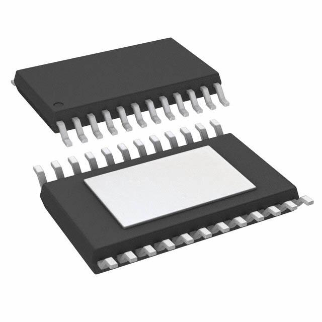


 工商网监
湘ICP备2023018690号
工商网监
湘ICP备2023018690号
